ISSN (Print) : 2320 – 3765 ISSN (Online): 2278 – 8875
I
nternational
J
ournal of
A
dvanced
R
esearch in
E
lectrical,
E
lectronics and
I
nstrumentation
E
ngineering
(An ISO 3297: 2007 Certified Organization)
Vol. 3, Issue 11, November 2014
Area-Delay Efficient Binary Adders in QCA
AngomSachindro Singh, V.Sreevani
P.G. Student (M-Tech) in VLSI & ES, GIET, Rajahmundry, A.P, India
Asst. Prof, M.Tech (VLSI & SD), Dept of ECE, GIET, Rajahmundry, A.P, India
ABSTRACT: In this paper, a novel quantum-dot cellular automata(QCA) adder design is presented that decrease the number ofQCA cells compared to previously report designs. Theproposed one-bit QCA adder design is based on a newalgorithm that requires only three majority gates and twoinverters for the QCA addition.A novel 128-bit adder designed in QCA was implemented. It achieved speed performances higher than all the existing. QCA adders, with an area requirement comparable with the cheap RCA and CFA established. The novel adder operates in the RCA fashion, but it could propagate a carry signal through a number of cascaded MGs significantly lower than conventional RCA adders. In adding together, because of the adopted basic logic and layout strategy, the number of clock cycles required for completing the explanation was limited. As transistors reduce in size more and more of them can be accommodated in a single die, thus increasing chip computational capabilities. However, transistors cannot find much smaller than their current size. The quantum-dot cellular automata approach represents one of the possible solutions in overcome this physical limit, even though the design of logic modules in QCA is not forever straightforward.
KEYWORDS: Adders, nano-computing, QCA (quantum-dot cellular automata)
I. INTRODUCTION
In this paper, a new QCA adder design is implemented thatreduces the number of QCA cells when compared to existingreported designs. We demonstrate that it is possible to design aCLA QCA one-bit adder, with the same reduced hardware asthe bit-serial adder, as retaining the simpler clockingscheme and parallel structure of the novel CLA approach.The proposed design is based on a new algorithm thatrequires only three majority gates and two inverters for theQCA addition. It is noted that the bit-serial QCA adder uses avariant of the proposed one-bit QCA adder. By connectnproposed one-bit QCA adders.
ISSN (Print) : 2320 – 3765 ISSN (Online): 2278 – 8875
I
nternational
J
ournal of
A
dvanced
R
esearch in
E
lectrical,
E
lectronics and
I
nstrumentation
E
ngineering
(An ISO 3297: 2007 Certified Organization)
Vol. 3, Issue 11, November 2014
Fig 1 Novel 2-bit basic module
An adder designed as proposed runs in the RCA fashion, but it exhibit a computational delay lower than all state-ofthe- art competitors and achieves the lowest area-delay product (ADP).
II. BACK GROUND
A. QCA Basics
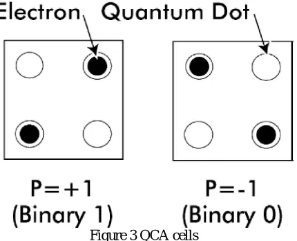
QCA is based on the interface of bi-stable QCA cellsconstructed from four quantum-dots. A high-level design oftwo polarized QCA cells is shown in Fig. 2. Each cell isconstructed from four quantum dots arranged in a squarepattern. The cell is charged with two electrons, which are free of chargeto tunnel between adjacent dots. These electrons tend totake up antipodal sites as a result of their mutual electrostaticrepulsion. Thus, there exist two equalenergeticallyminimal arrangements of the two electrons in the QCA cell asshown in Fig. 2. These two arrangements are denoted as cellpolarization P = +1 and P = -1 correspondingly. By using cellpolarization P = +1 to represent logic “1” and P = -1 torepresent logic “0”, binary information can be encoded.
Figure 3 QCA cells
ISSN (Print) : 2320 – 3765 ISSN (Online): 2278 – 8875
I
nternational
J
ournal of
A
dvanced
R
esearch in
E
lectrical,
E
lectronics and
I
nstrumentation
E
ngineering
(An ISO 3297: 2007 Certified Organization)
Vol. 3, Issue 11, November 2014
B. QCA Logical Devices
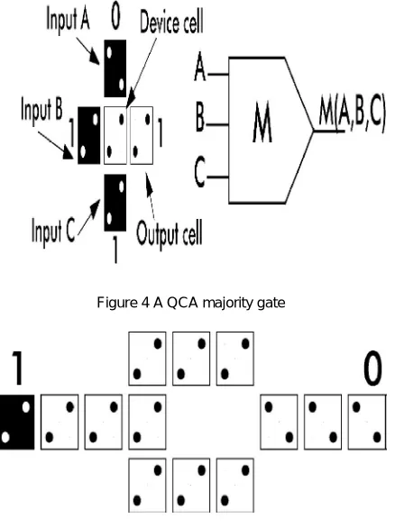
The fundamental QCA logic devices are the QCA wire,majority gate and inverter.
QCA wire: In a QCA wire, the binary signal propagatesfrom input to output because of the Columbicconnectionsbetween cells. This is a result of the system attempting to settleto a ground state. Any cells along the wire that are anti-polarizedto the input would be at a high energy level, andwould soon settle to the correct ground state. The propagationin a 90-degree QCA wire is shown in Fig. 4. Other than the 90-degree QCA wire, a 45-dgree QCA wire can also be used. Inthis case, the propagation of the binary signal alternatesbetween the two polarizations. Advance, there exists a so-callednon-linear QCA wire, in which cells with 90-degree orientationcan be placed next to one more, but off center.
Figure 3 A QCA wire (90-degree)
Majority gate and inverter: The majority gate andinverter are shown in Fig. 4 and Fig. 5 respectively. Themajority gate performs a three-input logic function. Assumingthe inputs are A, B and C, the logic function of the majoritygate is
m(A, B,C) = A|B + B|C + A|C (1)
By fixing the polarization of one input as logic “1” or “0”, wecan get an OR gate and an AND gate respectively. Morecomplex logic circuits can then be designed from OR andAND gates.
Figure 4 A QCA majority gate
ISSN (Print) : 2320 – 3765 ISSN (Online): 2278 – 8875
I
nternational
J
ournal of
A
dvanced
R
esearch in
E
lectrical,
E
lectronics and
I
nstrumentation
E
ngineering
(An ISO 3297: 2007 Certified Organization)
Vol. 3, Issue 11, November 2014
C. QCA Full Adders
Figure 6 one-bit QCA full adder
III. PROPOSED METHOD
A QCA is a nano-structure having as its basic cell a square four quantum dots structure charged with two free electrons able to tunnel through the dots inside the cell. Because of Coulombic repulsion, the two electrons will forever reside in opposite corners. The locations of the electrons in the cell determine two possible stable states that can be associated to the binary state 1 and 0.
ISSN (Print) : 2320 – 3765 ISSN (Online): 2278 – 8875
I
nternational
J
ournal of
A
dvanced
R
esearch in
E
lectrical,
E
lectronics and
I
nstrumentation
E
ngineering
(An ISO 3297: 2007 Certified Organization)
Vol. 3, Issue 11, November 2014
Several designs of adders in QCA exist in literature. The RCA [11], [13] and the CFA [12] process n-bit operands by cascading n full-adders (FAs). Even althoughthese addition circuits use different topologies of the genericFA, they include a carry-in to carry-out path consistingof one MG, and a carry-in to sum bit path containtwo MGs plus one inverter. As aimportance, theworst case computational paths of the n-bit RCA and then-bit CFA consist of (n+2) MGs and one inverter.A CLA design formed by 4-bit slices was also presented. In particular, the auxiliary propagate andgenerate signals, namely = + and = . ,are compute for each bit of the operands and then theyare grouped four by four. Such a designed n-bit CLA has acomputational path composed of 7+4×(log ) cascade MGsand one inverter. This can be easily verified by observing that,given propagate and generate signals, to compute grouped propagate and groupedgenerate signals; four cascade MGs are introduced in thecomputational path. In addition, to calculate the carry signals,one level of the CLA logic is required for each factor of fourin the operands word-length. This means that process nbitaddends, log levels of CLA logic are required, everycontributing to the computational path with four cascadedMGs. Finally, the calculation of sum bits introduces twofurther cascaded MGs and one inverter.The parallel-prefix BKA demonstrated exploitsmore efficient basic CLA logic designs. As its main
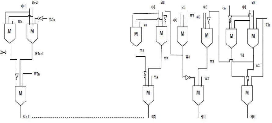
Novel 16-bit adder
advantage over the previously describe adders, the BKA can achieve lower computational delay. When n-bit operands are processed, its bad case computational path consists of 4×log −3 cascaded MGs and one inverter. Apart from the level required to compute propagate and generate signals, the prefix tree consists of 2 × log −2stages. From the logic equations provided, it can be easily verified that the first stage of the tree introduces in the computational path just one MG; the last stage of the tree contributes with only one MG; while, the intermediate stages introduce in the critical path two cascaded MGs all. Finally, for the computation of the sum bits, further two cascaded MGs and one inverter are added. With the main objective of trading off area and delay, the hybrid adder (HYBA) described combines a parallelprefix adder through the RCA. In the presence of n-bit operands, this architecture has a worst computational path consisting of 2 × log + 2cascade MGs and one inverter.When the methodology in recent timesproposed was exploited, the worst case path of the CLA is reduced to 4 × [log ]+ 2 × [log ]−1 MGs and one inverter. The above-mentioned approach can be applied also to design the BKA. In this case the overall area is reduced with respect to, but maintaining the same computational path. By applying the decomposition method demonstrated, the computational paths of the CLA and the CFA are reduced to 7 + 2 × log (n/8) MGs and one inverter and to (n/2) + 3 MGs and one inverter, respectively.
IV. NOVEL QCA ADDER
To introduce the novel design proposed for implementing ripple adders in QCA, let consider two n-bit addends A =
ISSN (Print) : 2320 – 3765 ISSN (Online): 2278 – 8875
I
nternational
J
ournal of
A
dvanced
R
esearch in
E
lectrical,
E
lectronics and
I
nstrumentation
E
ngineering
(An ISO 3297: 2007 Certified Organization)
Vol. 3, Issue 11, November 2014
Novel 32-bit adder
Novel 64-bit adder
= . , are computed being the carry produced at the generic (i−1)th bit position, the carry signal ci+2, furnished at the (i+1)th bit location, can be computed using the conventional CLA logic reported. The latter can be rewritten as given in (3), by exploiting Theorems 1 and 2 demonstrated. In this way, the RCA action, needed to propagate the carry through the two subsequent bit locations, requires only one MG. Conversely, conventional circuits operating in the RCA fashion, namely the RCA and the CFA, require two cascaded MGs to perform the same operation. In other words, an RCA adder designed as proposed has a worst case path almost halved with respect to the conventional RCA and CFA. Equation (3) is exploited in the design of the novel 2-bit module shown in Figure. 1 that also shows the computation of the carry = M( ). The proposed n-bit adder is then implemented by cascading n/2 2-bit modules as shown in Fig. 2(a). Having assumed that the carry-in of the adder is = 0, the signal is not required and the 2-bit module used at the least significant bit position is simplified.
ISSN (Print) : 2320 – 3765 ISSN (Online): 2278 – 8875
I
nternational
J
ournal of
A
dvanced
R
esearch in
E
lectrical,
E
lectronics and
I
nstrumentation
E
ngineering
(An ISO 3297: 2007 Certified Organization)
Vol. 3, Issue 11, November 2014
V. RESULTS
The proposed addition design is implemented for several operands word lengths using the QCA Designer tool adopting the same rules and simulation settings used.
Block diagram
ISSN (Print) : 2320 – 3765 ISSN (Online): 2278 – 8875
I
nternational
J
ournal of
A
dvanced
R
esearch in
E
lectrical,
E
lectronics and
I
nstrumentation
E
ngineering
(An ISO 3297: 2007 Certified Organization)
Vol. 3, Issue 11, November 2014
Technology schematic
ISSN (Print) : 2320 – 3765 ISSN (Online): 2278 – 8875
I
nternational
J
ournal of
A
dvanced
R
esearch in
E
lectrical,
E
lectronics and
I
nstrumentation
E
ngineering
(An ISO 3297: 2007 Certified Organization)
Vol. 3, Issue 11, November 2014
VI. CONCLUSION
A new adder designed in QCA was implemented. It achieved speed performances high than all the existing QCA adders, with an area requirement comparable with the cheap RCA and CFA demonstrated. The novel adder operated in the RCA fashion, but it could propagate a carry signal through a number of cascaded MGs significantly lesser than conventional RCA adders. In addition, because of the adopted basic logic and layout strategy, the number of clock cycles required for completing the explanation was limited. A 128-bit binary adder designed as described in this brief.
REFERENCES
[1] C. S. Lent, P. D. Tougaw, W. Porod, and G. H. Bernestein, “Quantum cellular automata,” Nanotechnology, vol. 4, no. 1, pp. 49–57, 1993. [2] M. T. Niemer and P. M. Kogge, “Problems in designing with QCAs: Layout = Timing,” Int. J. Circuit Theory Appl., vol. 29, no. 1, pp. 49–62, 2001.
[3] J. Huang and F. Lombardi, Design and Test of Digital Circuits by Quantum-Dot Cellular Automata. Norwood, MA, USA: Artech House, 2007.
[4] W. Liu, L. Lu, M. O’Neill, and E. E. Swartzlander, Jr., “Design rules for quantum-dot cellular automata,” in Proc. IEEE Int. Symp. CircuitsSyst., May 2011, pp. 2361–2364.
[5] K. Kim, K. Wu, and R. Karri, “Toward designing robust QCA architectures in the presence of sneak noise paths,” in Proc. IEEE Design,Autom.
Test Eur. Conf. Exhibit., Mar. 2005, pp. 1214–1219.
[6] K. Kong, Y. Shang, and R. Lu, “An optimized majority logic synthesis methology for quantum-dot cellular automata,” IEEE Trans.
Nanotechnol., vol. 9, no. 2, pp. 170–183, Mar. 2010.
[7] K. Walus, G. A. Jullien, and V. S. Dimitrov, “Computer arithmetic structures for quantum cellular automata,” in Proc. AsilomarConf.Sygnals,
Syst. Comput., Nov. 2003, pp. 1435–1439.
[8] J. D. Wood and D. Tougaw, “Matrix multiplication using quantumdot cellular automata to implement conventional microelectronics,” IEEE
Trans. Nanotechnol., vol. 10, no. 5, pp. 1036–1042, Sep. 2011.
[9] K. Navi, M. H. Moaiyeri, R. F. Mirzaee, O. Hashemipour, and B. M. Nezhad, “Two new low-power full adders based on majority-not gates,” Microelectron. J., vol. 40, pp. 126–130, Jan. 2009.
[10] L. Lu, W. Liu, M. O’Neill, and E. E. Swartzlander, Jr., “QCA systolic array design,” IEEE Trans. Comput., vol. 62, no. 3, pp. 548–560, Mar. 2013.
[11] H. Cho and E. E. Swartzlander, “Adder design and analyses for quantum-dot cellular automata,” IEEE Trans. Nanotechnol., vol. 6, no. 3, pp. 374–383, May 2007.
ISSN (Print) : 2320 – 3765 ISSN (Online): 2278 – 8875
I
nternational
J
ournal of
A
dvanced
R
esearch in
E
lectrical,
E
lectronics and
I
nstrumentation
E
ngineering
(An ISO 3297: 2007 Certified Organization)
Vol. 3, Issue 11, November 2014
pp. 721–727, Jun. 2009.
[13] V. Pudi and K. Sridharan, “Low complexity design of ripple carry and Brent–Kung adders in QCA,” IEEE Trans. Nanotechnol., vol. 11, no. 1, pp. 105–119, Jan. 2012.
[14] V. Pudi and K. Sridharan, “Efficient design of a hybrid adder in quantumdot cellular automata,” IEEE Trans. Very Large Scale Integr. (VLSI) Syst., vol. 19, no. 9, pp. 1535–1548, Sep. 2011.
[15] S. Perri and P. Corsonello, “New methodology for the design of efficient binary addition in QCA,” IEEE Trans. Nanotechnol., vol. 11, no. 6, pp. 1192–1200, Nov. 2012.
BIOGRAPHY
Mr. K Ravitheja received the B.Tech (ECE) from ANNAMACHARYA institute of Technology and science, Tirupati, India, JNTU Anantpur, India, in 2012 and pursuing M.Tech (ECE) specialization is DSCE from ANNAMACHARYA institute of Technology and science, Tirupati, India. Field of Interest VLSI and Embedded Systems.
Miss. G.Vasantha received the B.Tech (ECE) from SRI VIDYANIKETHAN College of Engineering TIRUPATI, JNTU Ananthapur, India, in 2007 and M.Tech (VLSI) from SVPCET Puttur, India, in 2011. Present she is currently working as an Assistant Professor in ANNAMACHARYA institute of Technology and science, Tirupati, India. She has been active in research and published 1 international journals& attended 1 National conferences in the field of Communications.