DC component Minimisation in Transformer
Less Three Phase Grid Connected Photo
Voltaic Inverters by Integral Method
Vinoth .R
1, Bhuvaneswari .C
2P.G. Student, Department of Electrical Engineering, PEC Engineering College, Vellore, Tamilnadu, India1
Assistant Professor, Department of Electrical Engineering, PEC Engineering College, Vellore, Tamil nadu, India2
ABSTRACT: The dc component can cause line-frequency power ripple, dc-link voltage ripple, and a further Second-order harmonic in the ac current. This paper has proposed an effective solution to minimize the dc component in three-phase ac currents and developed a software-based approach to mimic the blocking capacitors used for the dc component minimization, the so-called virtual capacitor. The “virtual capacitor” is achieved by adding an integral of the dc Component in the current feedback path. A method for accurate extraction of the dc component based on double time integral, as a key to achieve the control, has been devised and approved effective even under grid-frequency variation and harmonic conditions.
KEYWORD: Virtual capacitor, Transformer less, photovoltaic inverters, Integral method.
I.INTRODUCTION
Grid-connected photovoltaic (PV) systems often include a line transformer between the power converter and the grid. The transformer guarantees galvanic isolation between the grid and the PV systems, thus fulfilling safety standards. Furthermore, it ensures that no direct current (dc) is injected to the grid. However, the low-frequency (50 or 60Hz) transformer is bulky, heavy and expensive and its power loss brings down the overall system efficiency. To eliminate the transformer and achieve cost, size and weight reduction as well as efficiency improvement, the research and interest on „Transformer less‟ power conversion is growing There are several issues associated with transformer less structures, such as dc component in the inverter output (grid) current, ground leakage current (due to common-mode voltage and parasitic capacitance) and The voltage level mismatch between the solar panel (inverter) and grid. Among them, the dc component can affect the normal system operation and cause safety concerns. Standards have therefore been established in many countries to limit the level of the dc component, for example, below 0.5% of the rated output current (e.g. IEEE Std.1547-2003) therefore, this paper will investigate effective solutions to minimize the dc component in a PV system. The dc component can have negative impacts on the power system in the Following ways.
1) The dc component can affect the operating point of the transformers in the power system. The transformer cores are driven into unidirectional saturation with consequent larger excitation current. The service lifetime of the transformer is reduced as a result with further increased hysteresis and eddy current losses and noise.
2) The dc component can circulate between inverter phase legs as well as among inverters in a paralleled configuration. The dc component circulation affects the even current and loss distribution among paralleled inverters.
4) The corrosion of grounding wire in substations is intensified due to the dc component. There are several sources leading to the dc components in grid connected inverters: 1) asymmetry in the switching behavior of power semiconductor devices, 2) imparity in gate driver circuits, 3) device turn-on and turn-off delays, 4) non-identical device voltage drops (on-state resistance, saturation voltage, etc), 5) sampling biases from the ac current and ac voltage sensors, etc . Minimization of the dc component in transformer less PV inverters has been extensively investigated in literatures. Several solutions have been developed which can be grouped into two categories: passive methods and active methods. For example, coupling transformers and blocking capacitors are inserted on the inverter ac side to minimize the dc component.
II SYSTEM UNDER STUDY
GRID-CONNECTED photovoltaic (PV) systems often include a line transformer between the power converter and the grid. The transformer guarantees galvanic isolation between the grid and the PV systems, thus fulfilling safety standards. Furthermore, it ensures that no direct current (dc) is injected to the grid. However, the low-frequency (50 or 60 Hz) transformer is bulky, heavy, and expensive and its power loss brings down the overall system efficiency. To eliminate the transformer and to achieve cost, size, and weight reduction as well as efficiency improvement, the research and interest on “transformer less” power conversion is growing. There are several issues associated with transformer less structures, such as dc component in the inverter output (grid) current, ground leakage current (due to common-mode voltage and parasitic capacitance), and the voltage-level mismatch between the solar panel (inverter) and grid.
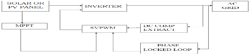
Block diagram for Dc component minimization. Among them, the dc component can affect the normal system operation and cause safety concerns. Standards have therefore been established in many countries to limit the level of the dc component, for example, below 0.5% of the rated output current (e.g., IEEE Standard 1547-2003). Therefore, this paper will investigate effective solutions to minimize the dc component in a PV system.
III VIRTUAL CAPACITORS
One way to block the dc component is to put a capacitor C in series with the ac side of the inverter as shown in.
However, in order to reduce the capacitive reactance at other frequencies, the capacitor value needs to be large, which
increasesthe size and cost of the system. This series capacitor may also affect the system dynamic response and reduce
transmission efficiency. Nevertheless, the physical capacitor can be replaced by software-based method and advanced control strategy which mimics the operation of the series capacitor in a single phase PV system.
Fig 1.2 PV inverters connected with virtual capacitors.
The current control loop diagram of the single-phase PV inverter with the blocking capacitor is shown in where the
reference is current; G is the controller transfer function, and KPWM is the gain of pulse width modulator. If the
capacitor voltage feedback terminal (1/Cs) is moved to the front of the pulse width modulator (KPWM), the control
diagram can be equivalently transformed to the structure shown in. As seen, the blocking capacitor C is replaced with an
integral and feedback block, the so-called virtual capacitor. This virtual capacitor can be implemented with software-based method and avoids the uses of physically large and expensive ac capacitors to block the dc component.
IV SPACE VECTOR PULSE WIDTH MODULATION
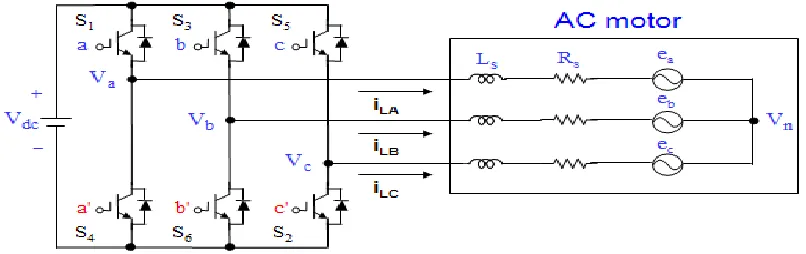
Space vector PWM is an advanced, computationally intensive technique that offers superior performance in variable-speed drives. This technique has the advantage of taking account of interaction among the phases when the load neutral is isolated from the center tap of the dc supply. Space vector PWM can be used to minimize harmonic content of the three-phase isolated neutral load.
When an upper switch is turned on (i.e., a, b or c is “1”), the corresponding lower switch is turned off (i.e., a', b' or c' is
“0”).Eight possible combinations of on and off patterns for the three upper transistors (S1, S3, S5)The eight
combinations, phase voltages and output line to line voltages
Table 1.1 Space Vector PWM Modulations.
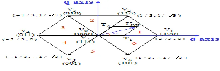
Fig 1.2 D-Q axis of SVPWM.
Treats the sinusoidal voltage as a constant amplitude vector rotating at constant frequency. This PWM technique
approximates the reference voltage Vref by a combination of the eight switching patterns (V0 to V7) Coordinate
Transformation (abc reference frame to the stationary d-q frame).A three-phase voltage vector is transformed into a vector in the stationary d-q coordinate frame which represents the spatial vector sum of the three-phase voltage.
V MPPTWITH PI CONTROLLER
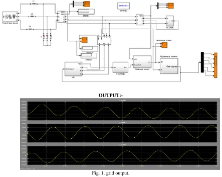
VI SIMULATIONS AND RESULTS
From the DC component minimization in transformer less used to get pure power to feed in an AC grid to impure of injecting the frequency power ripple, DC voltage ripple and further second order harmonics losses. To be maximum voltage dip to be compensated.
In the simulink model, this model is compensated by photo voltaic inverters there are further connected to identical loads so that their performance are fairly compared. The controller PI employed in the compensated feeder. The loads investigated in this work are static linear and static non-linear loads.
OUTPUT:-
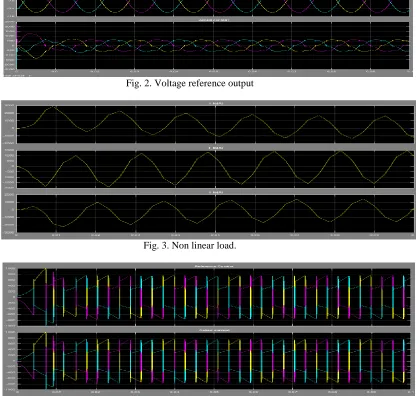
Fig. 2. Voltage reference output
Fig. 3. Non linear load.
Fig. 4. reference current.
VII CONCLUSION
based“Virtual capacitor” approach has been implemented to minimize the dc component via a feed-forward of the dc component. The dc component can be accurately obtained using the sliding window iteration and double time integral even under frequency variation and harmonic conditions. A PIR controller has been designed to enable the precise
regulation of both the dc and line-frequency components in the d-q frame. Experimental results have validated the
proposed method, where the dc component has been reduced below 0.5% and the dc-link voltage ripple has been attenuated as well. The proposed method can be well adopted in the existing PV systems for dc component minimization by adding software programs for dc-component extraction, dc-component feed forward term as well as the resonant controller in the current control loops.
REFERENCES
[1] R.Gonzalez, E. Gubia, J. Lopez, and L.Marroyo “Transformer less single phase multilevel-based photovoltaic inverter,” IEEE Trans. Ind. Electron.,vol. 55, no. 7, pp. 2694–2702, Jul. 2008.
[2] S. B. Kjaer, J. K. Pedersen, and F. Blaabjerg, “A review of single phasegrid-connected inverters for photo voltaic modules,” IEEE Trans. Ind.Appl., vol. 41, no. 5, pp. 1292–1306, Sep./Oct. 2005.
[3]E. Koutroulis and F. Blaabjerg,design optimization of transformer grid-connected PV inverters including reliability,” IEEE Trans. Power Electron., vol. 28, no. 1, pp. 325–335, Jan. 2013.
[4] B. Gu, J. Dominic, J. Lai, C. Chen, T. LaBella, and B. Chen, “High reliability and efficiency single-phase transformer less inverter for grid connected photovoltaic systems,” IEEE Trans. Power Electron., vol. 28, no. 5, pp. 2235–2245, May 2013.
[5] S. V. Araujo, P. Zacharias, and R. Mallwitz, “Highly efficient single Transformer less inverters for grid-connected photovoltaic systems,” IEEE Trans. Ind. Electron., vol. 57, no. 9, pp. 3188–3128, Sep. 2010
[6] O. Lopez, F. D. Freijedo, A. G. Yepes, P. Fernandez-Comesaa, J. Malvar, R.Teodorescu, and J. Doval-Gandoy, “Eliminating ground current in a transformer less photovoltaic application,” IEEE Trans. Energy Convers.,vol. 25, no. 1, pp. 140–147, Mar. 2010.
[7] V. Salas, E. Ol´ıas, M.Alonso, and F. Chenlo “Overview of the legislation of DC injection in the network for low voltage small grid-connected PVsystems in Spain and other countries,” Renewable Sustainable Energy Rev., vol. 12, no. 2, pp. 575–583, Feb. 2008.
[8] B. Wang, X. Guo, H. Wu, Q. Mei, and W. Wu, “Real-time DC injection Measurement technique for transformer less PV systems,” in Proc. IEEE2nd Int. Symp. Power Electron. Disturb. Generation Syst., Hefei, China, Jun. 2010, pp. 980–983.
[9] W. Li, L. Liu, T. Zheng, G. Huang, and S. Hui, “Research on effects of transformer DC Bias on negative sequence protection,” in Proc. Int.Conf. Adv. Power Syst. Automat. Protection, Beijing, China, Oct. 2011, pp. 1458–1463.
[10] A. Ah flock and A. J. Hewitt, “DC magnetization of transformers,” IEEE Proc.-Electro Power Appl., vol. 153, no. 4, pp. 601–607, Jul. 2006. [11] M. A. S. Masoum and P. S. Moses, “Impact of balanced and unbalanced Direct current bias on harmonic distortion generated by asymmetric three phase three-leg transformers,” IET Electro. Power Appl., vol. 4, no. 7, pp.507–515, Jul. 2010.
[12] F. Berba, D. Atkinson, and M. Armstrong, “A review of minimization of output DC current component methods in single-phase grid-connected inverters PV applications,” in Proc. 2nd Int. Symp. Environ. Friendly Energies Appl., Tyne, U.K., Jun. 2012, pp. 296–301.
[13] M. Armstrong, D. J. Atkinson, C. M. Johnson, and T. D. Abeyasekera, “Auto-calibrating DC link current sensing technique for transformer less, grid connected, H-bridge inverter systems,” IEEE Trans. Power Electron., vol. 21, no. 5, pp. 1385–1393, Sep. 2006.
[14] F. Berba, D. Atkinson, and M. Armstrong, “Minimization of DC current component in transformer less Grid-connected PV inverter application,” inProc. 10th Int. Conf. Environ. Elect. Eng., Rome, Italy, May 2011, pp. 1–4.