direction of Dr. Alexander Dean).
There are many studies seeking reduction of CPU utilization and improvement of
power consumption efficiency. For CPU utilization reduction, one effective solution is to
use event-based control to avoid unnecessary CPU operations. For power efficiency, a switch
mode power supply (SMPS) is widely used because it can efficiently convert an input voltage
to a different output voltage with low power loss.
In this thesis, a software SMPS controller is implemented for a boost converter to
regulate the output voltage. At the same time, we use event-based control and code
optimization methods to effectively reduce the CPU utilization for our voltage regulating task.
In the experimental section, we test the controlled boost converter with three kinds of loads
with different characteristics and demonstrate correct operation with much lower CPU
© Copyright 2014 by Si Li
by Si Li
A thesis submitted to the Graduate Faculty of North Carolina State University
in partial fulfillment of the requirements for the degree of
Master of Science
Electrical Engineering
Raleigh, North Carolina
2014
APPROVED BY:
_______________________________ ______________________________ Dr. Alexander Dean Dr. Subhashish Bhattacharya
Committee Chair
DEDICATION
To everyone who loves me in my life
Especially to my parents,
Mr. Xiaobo Li and Mrs. Yazhi Zhou,
BIOGRAPHY
Si Li was born on September 22, 1989 in Changchun, China. She had her undergraduate
study in Tongji University, Shanghai and received the degree of Bachelor in Electrical
Engineering in 2012. In the third year of undergraduate study, she began internship in United
Automotive Electronic Systems Co., Ltd. (UAES) and worked there for 8 months. After
graduation from Tongji University, she continued to pursue master degree in Electrical
Engineering in North Carolina State University since 2012. In the summer of 2013, she
joined Dr. Dean’s research group and was under his direction for thesis. In the thesis, her
concentration was embedded software implementation and power electronics. In the future
ACKNOWLEDGMENTS
I would like to first show my respect and appreciation to my advisors. I would like to thank
Dr. Alexander Dean for providing me the chance to work with him and for his valuable
guidance. From him, I gained a lot of research and practical experience. I would like to thank
Dr. Subhashish Bhattacharya for his help in power electronics. I would like to thank Dr.
James Tuck for his advice in code optimization. Also, I would like to thank my research
groupers. All of you have been helping me so much through my completion of thesis.
Especially I would like to thank Avik Juneja, Shikhar Singh, Udai Muhammed and Zhi Qu.
TABLE OF CONTENTS
LIST OF FIGURES ... viii
Chapter 1 INTRODUCTION ... 1
1.1 Motivation ... 1
1.2 Overview of the Research Contribution ... 1
1.3 Outline of the Thesis ... 2
Chapter 2 RELATED WORK ... 3
2.1 Boost Converter ... 3
2.2 PI Control ... 4
2.3 Event-Based Control ... 4
2.3.1 Årzén: Event-Based PID Controller [3] ... 4
2.3.2 Durand: An Event-Based PID Controller With Low Computational Cost [4] .... 6
2.3.3 Durand: Further Results on Event-Based PID Controller [5] ... 6
2.3.4 Xing: Some Improvements on Event-Based PID Controllers [6]... 7
Chapter 3 RESEARCH CONTRIBUTION ... 8
3.1 Boost Converter ... 8
3.1.1 Design ... 8
3.1.2 Operating Principles ... 9
3.2 Boost Converter Analysis ... 10
3.2.1 DC model analysis [7] ... 10
3.2.2 AC Small Signal Model Analysis [7] ... 12
3.3 PI Control Analysis and Implementation ... 13
3.3.2 MATLAB Implementation ... 15
3.3.3 PI Control Software Implementation ... 16
3.4 Event-Based (Dead-Band) Control Timing Analysis and Implementation ... 22
3.4.1 Event-Based Control Timing Analysis ... 22
3.4.2 Event-Based Control Implementation ... 29
3.4.3 Two Reference Voltages Implementation ... 30
3.5 CPU Usage Calculation Software Design ... 32
Chapter 4 EXPERIMENTAL EVALUATION AND SIMULATION ... 35
4.1 Simulation ... 35
4.2 Time-Triggered Control and Dead-Band Control ... 36
4.2.1 Test Load (Constant) ... 37
4.2.2 Test Load (Periodic) ... 40
4.2.3 Wi-Fi Module as Load ... 45
4.3 Analysis ... 52
4.3.1 Analysis for Constant Load ... 52
4.3.2 Analysis for Periodic Load ... 52
4.3.3 Analysis for Wi-Fi Module ... 53
Chapter 5 CONCLUSION AND FUTURE WORK ... 55
5.1 Conclusion ... 55
5.2 Future work ... 56
REFERENCES ... 57
Appendix A. Waveforms of Dead-Band Control with One Reference Voltage for the Periodically Changed Load ... 59
Appendix B. Waveforms of Dead-Band Control with Two Reference Voltages for the Periodically Changed Load ... 62
Appendix C. Waveforms of Dead-Band Control with One Reference Voltages for the Constant Load ... 65
Appendix D. Waveforms of Dead-Band Control with Two Reference Voltages for the Constant Load ... 67
LIST OF FIGURES
Figure 2-1 Boost converter circuit ... 3
Figure 2-2 Event-based control system [3] ... 5
Figure 3-1 Hand-built boost converter circuit ... 8
Figure 3-2 Boost converter circuit diagram ... 9
Figure 3-3 Equivalent circuit for 0 < t <= DT ... 11
Figure 3-4 Equivalent circuit for T < t <= T ... 11
Figure 3-5 Bode Plot before compensation ... 14
Figure 3-6 Bode Plot after compensation ... 15
Figure 3-7 Sequence diagram for ADC operation and control loop ... 16
Figure 3-8 Object code control flow graph ... 20
Figure 3-9 Blue trace shows time ADC ISR is active and executing control loop ... 21
Figure 3-10 Transient response in time-triggered control mode ... 23
Figure 3-11 Transient response in dead-band control in case Vini – Vrefl >ΔVO,R ... 25
Figure 3-12 Transient response in dead-band control in case Vini – Vrefl≤Δ VO,R ... 26
Figure 3-13 Transient response in dead-band control in never-fall-out case ... 27
Figure 3-14 Transient response of dead-band control in real situation, first fall-out point after ISR ... 28
Figure 3-15 Transient response of dead-band control in real situation, first fall-out point before ISR ... 29
Figure 3-16 Indication graph of three A/D conversion modes ... 30
Figure 3-17 Difference between one-reference-voltage mode and two-reference-voltage mode ... 31
Figure 4-1 Simulation circuit graph with PLECS ... 35
Figure 4-2 Simulation result ... 36
Figure 4-3 Constant load in time-triggered control: ISR indication and output ... 37
Figure 4-4 Constant load in dead-band control with one-reference-voltage mode in bands: 3.397V to 3.185V ... 38
Figure 4-5 Constant load in dead-band control with two-reference-voltage mode in bands: 3.397V to 3.185V ... 39
Figure 4-6 Periodical load in time-triggered control: transient response ... 41
Figure 4-7 Periodical load in time-triggered control: ISR indication graph with output ... 41
Figure 4-8 Periodical load in dead-band control with one-reference-voltage mode in bands: 3.397V to 3.185V ... 42
Figure 4-9 Periodical load in dead-band control with one-reference-voltage mode in bands: 3.397V to 3.185V ... 44
Figure 4-10 Wi-Fi module: initial state and steady state ... 46
Figure 4-11 Wi-Fi module: initial state ... 46
Figure 4-12 Wi-Fi module: steady state... 47
Figure 4-13 Wi-Fi module: one-reference-voltage mode with bands 3.326V to 3.255V ... 47
Figure 4-14 Wi-Fi module: two-reference-voltage mode with bands 3.326V to 3.255V... 48
Figure 4-15 Wi-Fi module: one-reference-voltage mode with bands 3.350V to 3.232V ... 48
Figure 4-16 Wi-Fi module: two-reference-voltage mode with bands 3.350V to 3.232V... 49
Figure 4-17 Wi-Fi module: one-reference-voltage mode with bands 3.373V to 3.208V ... 50
Figure 4-18 Wi-Fi module: two-reference-voltage mode with bands 3.373V to 3.208V... 50
Figure 4-19 Wi-Fi module: one-reference-voltage mode with bands 3.397V to 3.185V ... 51
Figure 4-20 Wi-Fi module: two-reference-voltage mode with bands 3.397V to 3.185V... 51
Figure 4-22 Analysis: CPU usage of periodical load... 53
Figure 4-23 Analysis: CPU usage of Wi-Fi module ... 54
Figure 5-1 Periodical load in dead-band control: one-reference-voltage, dead bands 3.326V to 3.255V, zoom-out version ... 59
Figure 5-2 Periodical load in dead-band control: one-reference-voltage, dead bands 3.326V to 3.255V, zoom-in version ... 59
Figure 5-3 Periodical load in dead-band control: one-reference-voltage, dead bands 3.350V to 3.232V, zoom-out version ... 60
Figure 5-4 Periodical load in dead-band control: one-reference-voltage, dead bands 3.350V to 3.232V, zoom-in version ... 60
Figure 5-5 Periodical load in dead-band control: one-reference-voltage, dead bands 3.373V to 3.208V, zoom-out version ... 61
Figure 5-6 Periodical load in dead-band control: one-reference-voltage, dead bands 3.373V to 3.208V, zoom-in version ... 61
Figure 5-7 Periodical load in dead-band control: two-reference-voltage, dead bands 3.326V to 3.255V, zoom-out version ... 62
Figure 5-8 Periodical load in dead-band control: two-reference-voltage, dead bands 3.326V to 3.255V, zoom-in version ... 62
Figure 5-9 Periodical load in dead-band control: two-reference-voltage, dead bands 3.350V to 3.232V, zoom-out version ... 63
Figure 5-10 Periodical load in dead-band control: two-reference-voltage, dead bands 3.350V to 3.232V, zoom-in version ... 63
Figure 5-11 Periodical load in dead-band control: two-reference-voltage, dead bands 3.373V to 3.208V, zoom-out version ... 64
Figure 5-12 Periodical load in dead-band control: two-reference-voltage, dead bands 3.373V to 3.208V, zoom-in version ... 64
Figure 5-14 Constant load in dead-band control: one-reference-voltage, dead bands 3.350V to 3.232V... 65
Figure 5-15 Constant load in dead-band control: one-reference-voltage, dead bands 3.326V to 3.255V... 66
Figure 5-16 Constant load in dead-band control: two-reference-voltage, dead bands 3.373V to 3.208V... 67
Figure 5-17 Constant load in dead-band control: two-reference-voltage, dead bands 3.350V to 3.232V... 67
Chapter 1 INTRODUCTION 1.1 Motivation
This thesis project focuses on event-based PI control and feed forward control of a switching
power converter which is controlled by an RL78/G14 16-bit single-chip microcontroller.
Switching power converters are used to convert power efficiently between voltages; this
enables power optimization by operating circuits at lower voltages. A control system is used
to improve the converter’s output accuracy in the face of changes in output load and input
voltage. This control system can be implemented in dedicated hardware (e.g. digital logic or
analog hardware) or in software on the MCU. The purpose of the project is to reduce the
CPU usage of a software implementation by reducing the number of times the control system
must execute.
1.2 Overview of the Research Contribution
My first contribution is in the development and analysis of the boost converter. I studied
power electronics and moved on to the boost converter we use in the project. I began with
hardware by studying and changing a boost converter circuit (developed by a previous
graduate student for driving high-brightness LEDs, which require current regulation) and
then made changes to fit this project (voltage regulation) better. Second, to achieve a constant
output voltage, the system needed a reliable control system. I analyzed the boost converter
circuit, built the DC and AC model with the loss elements and derived the transfer function
of the output voltage against transistor duty cycle. Next I took advantage of the sisotool
function in MATLAB to generate the Bode plot, and tuned it to get a stable system.
My second and main contribution is an analysis of methods to reduce CPU usage. The
control loop is very CPU-intensive. To reduce CPU usage, the system should use less time on
the control loop. The solution is event-based control. Rather than trigger the control loop
actual output voltage and the desired voltage. This control method is called dead-band
control.
The third contribution is how to implement dead-band control, making use of the existing
peripherals in the MCU. In RL78/G14, the A/D converter has two modes of interrupts. The
first mode causes an interrupt happens every time the A/D conversion finishes. The second
causes an interrupt when A/D conversion result is out of a specified range. The second mode
meets the dead-band control requirement, so we use it in this project.
1.3 Outline of the Thesis
The rest of the thesis has the following structure: In Chapter 2, I will describe some related
research on event-based control. In Chapter 3, I will introduce my contribution in this thesis
project. In Chapter 4, related experiments, simulations and application are presented. In
Chapter 2 RELATED WORK
In this chapter, I will introduce the boost converter and previous research in event-based
control. The research of Årzén is the basis of the other two.
2.1 Boost Converter
The boost converter is a basic class of switch mode power supply (SMPS) (Erickson &
Maksimovic, 2001). The output voltage is higher than the input voltage. The boost converter
consists of at least two semiconductors, which are diode and transistor. It also contains at
least one power storage element, which is inductor and capacitor. The ideal asynchronous
boost converter has the circuit shown in Figure 2-1.
Figure 2-1 Boost converter circuit
The transistor is driven by PWM signal, whose duty cycle is D. The output and input voltage
have the idealized relationship [1] [2]:
This relationship ignores effects from changes in load resistance, parasitic circuit elements
2.2 PI Control
Because the idealized model above ignores various realities, a closed-loop control system is
typically used to control the duty cycle in order to regulate the output voltage (minimizing
the error from the set point).
PI and PID controllers are often used for feedback control. PI stands for proportional and
integral, while PID adds a derivative term. The basic PID control has the format as follows [3]
[4]:
The proportional term KP provides a control action proportional to the error. Increasing the
proportional parameter will decrease the rising time and the settling time, but increase the
overshoot and instability.
The integral term KI will reduce the steady-state error. Increasing the integral parameter will
largely decrease the steady-state error, slightly decrease the rising time, but increase the
overshoot and instability.
The derivative term KD provides a control action proportional to the rate of change of the
error. This term also decreases the rising time and the settling time, but increase the
overshoot and instability.
I used the PI controller because it is adequate for the boost converter control and less
computationally intensive than the PID controller.
2.3 Event-Based Control
2.3.1 Årzén: Event-Based PID Controller [3]
Årzén’s event-based control system is designed as a client-server structure, as shown in
frequency, the time period is hnom. The PID controller works as the server, which is an
event-triggered mechanism. It is only event-triggered when the output of Event Detector meets the event
trigger requirements.
Figure 2-2 Event-based control system [3]
The PID controller is based on classic PID control theory and has the same structure as the
classic PID controller. It consists of proportional part, integral part and derivative part. The
difference between the conventional PID controller and the proposed one is that the PID
coefficients have to be recalculated every time the control implements. The reason is that
discretization needs frequency information, the event-based control has a sampling frequency
which is not fixed and is irregularly changed.
The sampling frequency changes according to the following rule: at each normal sampling
period, control sampling period hact changes to the summation of current hact and normal
sampling period hnom. If hact becomes larger than a limit hmax or event-based control is
2.3.2 Durand: An Event-Based PID Controller With Low Computational Cost [4]
Durand’s research builds on Årzén’s and is focused on lowering computational requirements.
They achieve the goal by setting a minimum sampling interval condition. In Årzén’s research,
if the triggering event doesn’t occur for several normal sampling periods, the control will
execute every sampling period. Although this will achieve the desired result, it costs many
computations. If control time demand is not very strict, the minimum sampling period could
be defined, and execution sampling period should be longer than the minimum sampling
period.
After the transient, although the output error is less than the triggering error limit, it still has
some oscillations due to lack of control. Durand’s solution is to add some extra samples right
after the transient, to make the error smaller and the system more stable.
2.3.3 Durand: Further Results on Event-Based PID Controller [5]
In this research, a hybrid algorithm is introduced to save control samples. It focuses on
integral part of PID control. In Årzén’s research, when triggering error limit increases, the
output oscillates after the transient response. The result comes from a problem in integral part.
In Årzén’s research, the forward difference approximation is implemented to calculate the
integral part. This method is a good approach in time-triggered PID control, but it is not a
proper choice in event-based control. In Durand’s research, it changes the approach into
backward difference approximation. Based on this change, it combines two algorithms to
ensure the reliability of the integral part. The first algorithm is to saturate product of h(tk)
and e(tk) when hact > hmax. When implementing this algorithm along, the output has almost
the same overshoot as in time-triggered PID control. The second algorithm is to add a
forgetting factor of the sampling period. This will result in that the control sampling period
approaches normal sampling period during transient response. In steady state intervals, the
control sampling period will be exponentially decreased, which will reduce the impact to the
control signal. This algorithm will cause larger overshoot than conventional discrete PID
After combination of the two algorithms, the output has fewer oscillations, and has modest
and reasonable overshoot.
2.3.4 Xing: Some Improvements on Event-Based PID Controllers [6]
This research is based on Årzén’s and Durand’s researches and has a few improvements.
They apply trapezium difference approximation other than forward difference approximation
in Årzén’s research and backward difference approximation in Durand’s research. For the
steady-state sampling condition, besides the condition , they use an additional
condition . When the system satisfies the first condition, if it also satisfies the second
one, the system will trigger the controller to calculate the new control signal. This method
will keep the static error converge to . In addition to the improvement above, they also
judge the step of sampling sensor . If is dividable by an unchanged integer , the
controller will be triggered. By experiment results, they also propose that increasing
properly will reduce a lot of sampling numbers. After applying those improvements, the
Chapter 3 RESEARCH CONTRIBUTION
My research is in the software design of a switch mode power supply system built on a boost
converter. The contributions include event-based control timing analysis and implementation;
boost converter analysis; PI control; analysis of using one or two reference voltages,
implementation and CPU usage calculation software design.
3.1 Boost Converter 3.1.1 Design
Figure 3-1 and Figure 3-2 shows the boost converter we use in this thesis. In which the
hand-build hardware and the circuit schematics are presented respectively.
Figure 3-2 Boost converter circuit diagram
3.1.2 Operating Principles
This is an asynchronous boost converter with load switching part. The output voltage is
related with MOSFET switching duty cycle and input voltage. Recall that ideal relationship
between the output voltage and the input voltage and the boost converter switch’s duty cycle
D is [1] [2]:
The input capacitor C1 is used to reduce the overall noise to ensure a better performance.
Output capacitor C2 reduces the output voltage ripple.
The boost converter MOSFET FET1 is driven by a pulse-width-modulated signal generated
by channels 0 and 1 of a Timer Array Unit. The duty cycle is adjusted by implementing PI
control on slave channel register value.
Diode D1 switches on automatically when FET1 is off, enabling the current from inductor L1
The MOSFET FET2 on the board is used to change the load periodically, introducing load
transients which are used to evaluate the system’s ability to minimize the output voltage error.
FET2 is driven by channel 2 of Timer Array Unit, which generates a square wave. When the
output voltage level is high, the additional load resistor R1 is connected in parallel with the
original load R2. When the output voltage level is low, the additional load R1 is disconnected
from the circuit.
3.2 Boost Converter Analysis
In this circuit, several loss elements have to be considered.
a. Inductor Copper Loss, Series Resistor RL
b. Capacitor loss RC
c. Semiconductor on-resistance Ron
d. Forward Voltage Drop VD
The circuit containing all the loss elements above is shown below. We consider the two states
of the circuit: when FET1 is on and when it is off.
3.2.1 DC model analysis [7]
(1)
Figure 3-3 Equivalent circuit for 0 < t <= DT
(2)
In this case, the equivalent circuit is shown in Figure 3-4.
3.2.2 AC Small Signal Model Analysis [7]
Equalizing the DC components gives:
=0
From the equations above, considering the loss elements, the boost converter DC model is:
The AC equivalent circuit model is
The equalized elements have these relationships with the DC and AC parts:
;
;
;
;
;
Next, we set to 0
in which,
3.3 PI Control Analysis and Implementation
We use this transfer function to design a compensator (a control system) using both
theoretical method and also with the help of MATLAB and its tool box.
3.3.1 Theoretical Method [7]
In this section, we first use MATLAB function tf() to generate the continuous
control-to-output transfer function Gvd(s), and take advantage of the function sisotool() to generate the
Figure 3-5 Bode Plot before compensation
According to the PI compensator design method, the compensator should be in the format of:
Because the PWM transistor switching frequency is 50kHz, we need to set the crossover
frequency fc = fsw/10 = 5kHz = 31k rad/sec. So we set the compensator gain to 0.2 in
order to compensate the magnitude at 31k rad/sec to 0 dB. Second, we should choose a value
for which is sufficiently small. In this case, we set = 100. The compensated Bode Plot
Figure 3-6 Bode Plot after compensation
3.3.2 MATLAB Implementation
We first find the discrete transfer function of output voltage to duty cycle by using
MATLAB’s c2d() function and this boost converter analysis. We then use the discrete
transfer function as the input of the sisotool() function, and tune the PI control compensator
parameters according to the Bode Plot generated. The PI compensator in MATLAB has the
format:
3.3.3 PI Control Software Implementation
We implemented the control loop in C code for the RL78 MCU.
3.3.3.1Timing Overview
The timing sequence of the software control implementation is shown in Figure 3-7.
Figure 3-7 Sequence diagram for ADC operation and control loop
When the ADC result meets the interrupt triggering condition (to be described below), the
A/D Interrupt is generated and the A/D interrupt service routine executes, which performs the
PI Control Loop.
3.3.3.2PI Control Loop Source Code
The idea to implement the software is to use fixed point math, shifts, and approximation to
eliminate the float point calculation. In this way, we can avoid as many call functions as
possible and reduce the code run time.
The approximations are implemented in the following two lines:
The approximation is that when an integer variable is multiplied by a float, we can split the
float number into several integers and decimal numbers which are equal to two to the power
of some integers.
The fixed point technique changes the float point number into a proper fixed point number
number and define the highest two bits as integer part, the other bits as decimal part, we need
to multiply the input value by 214.
3.3.3.3Object Code of Control Loop
The object code of the control loop part is shown in Appendix E.
According to the object code, the control flow graph reflecting the relationship between
38 HS_0 17 11 HS_1 8 HS_2 7 HS_3 21 7 HS_4 21 3 5 HS_5 7 HS_6 21 7 21 HS_7 3 12 HS_8 4 HS_9 1 5 HS_10 5 5 HS_11 HS_12 7 6 35 end entry
If we take time-triggered control mode as an example, according to the control flow graph,
the number of cycles for this case is 128 (before the calculation of CPU usage parameters),
divide the number with the system clock frequency, which is 32MHz, the time-triggered
control mode ISR needs 4µs.
3.3.3.4 Execution Time of Control Loop
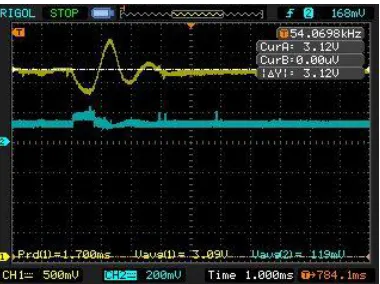
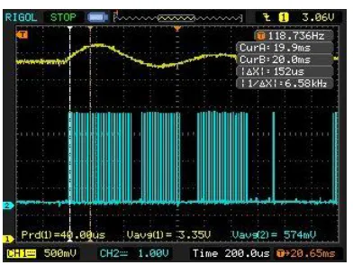
According to the analysis of object code, the analytical ISR routine time is about 4µs.
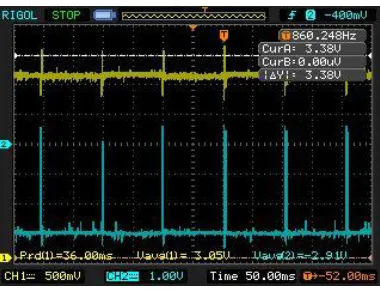
Besides this method, we can also get the control execution time by experiment. Figure 3-9
shows the time-triggered control execution time from the oscilloscope, in which the
execution time is also about 4µs, which matches with the analytical result.
3.4 Event-Based (Dead-Band) Control Timing Analysis and Implementation
With the time-triggered PI control loop code given above as a starting point, we now proceed
to examine how to reduce its use through event-based control.
3.4.1 Event-Based Control Timing Analysis
We wish to understand how the boost converter and controller respond to a step increase in
load current (a load transient of ΔIout), which is shown in Figure 3-10. In sampling-triggered
control policy with one reference voltage, the output voltage transient response is shown in
the following figure. To simplify the analysis, we assume that the load transient is
synchronized with the switching cycle. This assumption can be removed easily in future
ΔVO,R
Vrefl
tISR
PWM
ΔIout
Figure 3-10 Transient response in time-triggered control mode
In this project, the event-triggered (also called dead-band) control is used. Because it needs
some time for the output voltage to go out of the bounds, the timing analysis thus has some
additional delay and special characteristics compared with normal control.
The analysis will be based on the situation that the output current has a sudden increase.
There are three cases according to the relationship among the output voltage before the
transient response (Vini), the lower bound of the deadband (Vrefl) and the voltage drop in the
first phase of the transient response (Δ VO,R). In the first case, the absolute value of Vini - Vrefl
is larger than the first phase of voltage change, but the output voltage will still go out of the
phase of voltage change. In the third case the transient response process never goes out of the
deadband.
From Peterchev’s and Redl’s research [4], Δ VO,R is proportional to the change of the current
Δ I, which follows the equation below:
Δ VO,R =Δ IRC
Because Δ I results from a sudden load resistor change in my project, it follows the
relationship below, assuming this is the optimal control system and that the load resistor has
a sudden decrease which causes voltage output transient response.
Δ I = Iafter - Ibefore
Iafter = Vo/Ro,after
Ibefore = Vo/Ro, before
3.4.1.1Timing Analysis with Averaged Output Voltage
a. Case 1: Vini – Vrefl >Δ VO,R
ΔVO,R
Vrefl
Vrefu
tISR
PWM
Figure 3-11 Transient response in dead-band control in case Vini – Vrefl >ΔVO,R
In this case, the ADC will delay for one period, because ADC only occurs at the beginning of
the PWM period. The PWM duty cycle will be updated at the end of the same period where
the ADC triggers an interrupt. The output voltage begins to rise at the next period.
b. Case 2: Vini – Vrefl≤Δ VO,R
tISR
PWM
Vini
ΔVO,R
Vrefl
Vrefu
Figure 3-12 Transient response in dead-band control in case Vini – Vrefl ≤ΔVO,R
In this case, ADC will trigger an interrupt just in the PWM period where the voltage begins
to change, because the voltage drops out of the band at the very beginning of the response.
The voltage will rise at the next period.
c. Case 3: The output transient response doesn’t fall out of the dead bands.
Vini
ΔVO,R
Vrefl
Vrefu
tISR
Figure 3-13 Transient response in dead-band control in never-fall-out case
In this case, the output voltage will perform like the open-loop voltage response. The time
period from the beginning of the voltage change to the point when the voltage comes to
another steady state. The settling time and the voltage change between the two steady
states can be estimated by the following equations:
3.4.1.2Timing Analysis When Ripple Is Considered
The situations above are based on average output voltage. The real situation includes ripple
caused by PWM signals. In Figure 3-14, the blue signal is the output voltage with the ripples.
The black signal is the average output voltage. As shown in Figure 3-14, from the view of the
controller will work at the third period. If the ripple is considered, the real output will fall out
of the dead-band earlier than the averaged output but the fall-out points are always in the
same period. If the fall-out points of the real output voltage and the averaged output voltage
are both later than ISR run period, the controller will still begin to work in the third period. If
the out point of the real output voltage locates within the ISR but the average output
fall-out point doesn’t, the controller will begin to work one period earlier.
ΔVO,R
Vrefl
Vrefu
Δt
tISR
PWM
ΔVO,R
Vrefl
Vrefu
Δt
tISR
PWM
Figure 3-15 Transient response of dead-band control in real situation, first fall-out point before ISR
3.4.2 Event-Based Control Implementation
In this project, the event-based control is implemented by making use of a special A/D
Figure 3-16 Indication graph of three A/D conversion modes
Figure 3-15 shows two A/D conversion interrupt trigger modes, selected by the control bit
ADCRK. Mode 1 is that interrupt is triggered when A/D result is within a range; mode 2-3 is
the interrupt is triggered when A/D result is out of a preset range. The decision is made by
checking two 8-bit registers: ADUL and ADLL, which are the pre-written values and will be
compared with the highest 8 bits of A/D conversion result ADCR. The register storing that
highest 8 bits of ADCR is ADCRH. ADUL is the upper bound, ADLL is the lower one.
To implement event-based control, we use A/D converter to convert output voltage to digital
value, set A/D conversion interrupt trigger mode in mode 2-3 and set ADUL/ADLL as the
highest 8 bits of the value converted from the dead band value by the same rule as of the
output voltage converting to ADCR. When ADCRH is larger than ADUL or smaller than
ADLL, the interrupt is triggered and the control is implemented, i.e., the event-based control
is implemented.
3.4.3 Two Reference Voltages Implementation
Because in the project, band control is implemented, steady state error within the
applied. The error from the middle of the bands to the real output is larger than the error from
the closer dead-band edge to the output. If one reference voltage is applied, the error is
potentially larger than the error calculated when two reference voltages are applied. Larger
error will lead to a larger control signal, which can create a larger oscillation of the output
signal. To avoid oscillation in steady state as much as possible, I apply two reference
voltages in the project.
The difference of the results with one and two reference voltages is shown in Figure 3-16.
Vref Vmax
Vmin
CPU running
ΔI
Vrefu
Vrefl
Vmax
Vmin
CPU running
ΔI
3.5 CPU Usage Calculation Software Design
Timing diagram of CPU usage calculation software design is shown in Figure 3-17.
There are three interrupt sources related in this software design. The first interrupt source is a
timer interrupt triggered every 1 microsecond, which uses channel 0 in Timer Array Unit 1.
Entering this interrupt means the hardware counter counts down to zero and will be reset to
the upper bound . The second interrupt source is a timer interrupt triggered every 20
millisecond, which uses channel 2 in Timer Array Unit 1. When entering this interrupt, CPU
usage is calculated, afterwards the Cpu_Counter will be reset to zero. The third interrupt
source is ADC interrupt. When the A/D conversion finishes, if the output voltage falls out of
the bands, the system will enter this interrupt and implement PI control.
The hardware counter interrupt and the ADC interrupt have the highest priority. When the
system enters ADC interrupt, we capture the hardware counter values at the beginning and
the end of the ISR routine, and subtract the two values to get the ISR routine time.
Summarize the ISR routine time together throughout 20 ms. The summation is stored in the
Chapter 4 EXPERIMENTAL EVALUATION AND SIMULATION 4.1 Simulation
In the project, I use PLECS to simulate the closed loop control performance. The simulation
circuit and connection is in Figure 4-1.
For the transfer function part, I use the following function:
The simulation output is in Figure 4-2.
Figure 4-2 Simulation result
4.2 Time-Triggered Control and Dead-Band Control
In this part, we will look at and compare two types of control strategies: time-triggered
control, which is implemented at the beginning of every sampling period; and dead-band
control, in which control is only performed when the voltage goes out of the dead-band.
After showing the waveform, we will see the difference of the CPU usage between them.
The CPU usage can be viewed and calculated in a direct way. In both control strategies,
control will only be applied at the beginning of some sampling periods. If we use a digital
output port bit, set it to 1 when the control is applied, reset it to 0 when control is finished,
the waveform of this port bit will have the same length of the high level time in a specific
situation. The method to estimate CPU usage is to count the number of control loop run times,
multiply it by the control loop execution time, and divide the result by the measurement time
period.
Next, we will look at the output waveforms and their corresponding CPU usage of three
kinds of load: constant load, periodically changed load and a real Wi-Fi module load. In each
kind of load case, we will show one sub case in detail, and put the waveforms of the other
In the end, we will come to summarize and analyze the experiment results, sort them into
three graphs, showing the relationship between the output voltage and the size of the dead
band in three types of control.
4.2.1 Test Load (Constant)
We first observe and compute the CPU usage of the constant load case in time-triggered
control mode, dead-band control mode with one reference and dead-band control mode with
two reference voltages. The constant control is a resistant load with the resistance of 47 .
The desired output voltage is 3.3V.
4.2.1.1Time-Triggered Control
In the time-trigger control, the output waveform with the control loop running is shown in
Figure 4-3.
Figure 4-3 Constant load in time-triggered control: ISR indication and output
The control is triggered once every 20 . The control execution time is about 4 . So CPU
4.2.1.2Dead-Band Control
4.2.1.2.1 Dead-Band Control with One Reference Voltage
We will look at the waveform of the first case. The rest of the waveforms are listed in
Appendix C.
a. Dead-band: 3.397V to 3.185V
The output against ISR indication is shown in Figure 4-4.
Figure 4-4 Constant load in dead-band control with one-reference-voltage mode in bands: 3.397V to 3.185V
Number of control times: 0;
CPU usage is 0.
b. Dead-band: 3.373V to 3.208V
Number of control times: 0;
CPU usage is 0.
Number of control times: 9;
Control execution time is 4.4μ s; CPU usage is 0.00198.
d. Dead-band: 3.326V to 3.255V
Number of control times: 32;
Control execution time is 4.4μ s; CPU usage is 32*4.4/20000 = 0.00704.
4.2.1.2.2 Dead-Band Control with Two Reference Voltages
a. Dead-band: 3.397V to 3.185V
The output against ISR indication is shown in Figure 4-5.
Figure 4-5 Constant load in dead-band control with two-reference-voltage mode in bands: 3.397V to 3.185V
Number of control times: 0;
CPU usage is 0.
Number of control times: 0;
CPU usage is 0.
c. Dead-band: 3.350V to 3.232V
Number of control times: 6;
Control execution time is 4.4μ s; CPU usage is 0.00132.
d. Dead-band: 3.326V to 3.255V
Number of control times: 40;
Control execution time is 4.4μs;
CPU usage is 40*4.4/20000 = 0.0088.
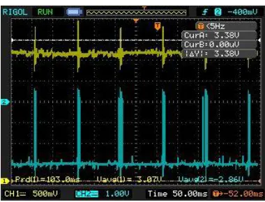
4.2.2 Test Load (Periodic) 4.2.2.1Time-Triggered Control
In the sampling-triggered control, there is only one reference voltage and no dead band. The
control frequency is the same as the sampling frequency. In this experiment, we set the
sampling frequency as 50 kHz, and the reference voltage as 3.3V. There are two 47Ω resistor
loads. One is the fixed load which is always connected between the output voltage and the
ground. The other is the switching load which will only be connected between the output
voltage and the ground when the MOSFET is on.
The output voltage (the blue signal) against the load change (the yellow signal) has the
Figure 4-6 Periodical load in time-triggered control: transient response
The waveform indicating CPU usage is in Figure 4-7.
Figure 4-7 Periodical load in time-triggered control: ISR indication graph with output
4.2.2.2Dead-Band Control
In the dead-band control, we have the same fixed resistor load and switching load. The
following experiments will be divided into two groups: dead-band control with one reference
voltage; and dead-band control with two reference voltages. To be succinct, I will only show
one case in detail in each group, including the related waveform and CPU usage computation
process. The waveforms of the rest cases are listed in Appendix. The CPU usage results are
shown in the analysis part.
4.2.2.2.1 Dead-Band Control with One Reference Voltage
In this case, the reference voltage is set to 3.3V and the dead-band is set to different widths.
We will observe the following four sub cases.
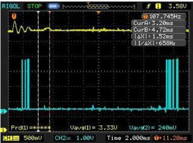
a. Dead-band: 3.397V to 3.185V
The waveform and CPU usage indication is shown in Figure 4-8.
There are 39 control execution times in average during one load switching period. The
Control execution time is about 4μ s. So CPU usage is about 39 *4/20000 = 0.0078.
b. Dead-band: 3.373V to 3.208V
Number of control times: 60;
Control execution time is 4μ s; CPU usage is 60*4/20000 = 0.012.
c. Dead-band: 3.350V to 3.232V
Number of control times: 130;
Control execution time is 4μ s; CPU usage is 130*4/20000 = 0.026.
d. Dead-band: 3.326V to 3.255V
Number of control times: 245;
Control execution time is 4μ s; CPU usage is 245*4/20000 = 0.049.
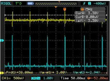
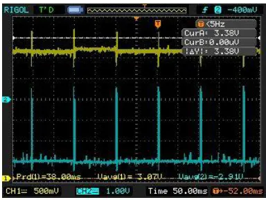
4.2.2.2.2 Dead-Band Control with Two Reference Voltages
In these cases, the reference voltage is set to be the closer edge of the dead-band. We will
observe the waveforms and CPU usage of one case. The waveforms of the rest three cases
are in Appendix B.
a. Dead bands are 3.397V to 3.185V
Figure 4-9 Periodical load in dead-band control with one-reference-voltage mode in bands: 3.397V to 3.185V
Number of control times: 24;
Control execution time is 4μ s; CPU usage is 24*4/20000 = 0.0048.
b. Dead-band: 3.373V to 3.208V
Number of control times: 42;
Control execution time is 4μ s; CPU usage is 42*4/20000 = 0.0084.
c. Dead-band: 3.350V to 3.232V
Number of control times: 96;
Control execution time is 4μ s; CPU usage is 96*4/20000 = 0.0192.
d. Dead-band: 3.326V to 3.255V
Number of control times: 168;
4.2.3 Wi-Fi Module as Load
After evaluating the performance of the dead-band control on a synthetic, periodic load, we
wish to evaluate its performance on a real application with more complicated power
requirements. We use the Gainspan GS1011MIPS Wi-Fi module, which is built into the
RDK development board. This module operates at 3.3 V and draws a wide range of currents
based on radio activity (receiving, transmitting, idle).
In this experiment, the boost converter powers the Wi-Fi module on the other G14 RDK,
which is actively sending and receiving data. To sense the voltage change in accordance to
the current change, a current sensing resistor placed in series between the voltage output pin
of the boost converter, and voltage input pin of the Wi-Fi module. The graph is shown below.
When Wi-Fi module transmits signals, the input current of the Wi-Fi module changes with
the signals. The input voltage of Wi-Fi module will change with the current change.
The following experiment results show the initial setup state of Wi-Fi module and the steady
state after setting up. The first experiment is based on that the system uses two reference
voltage dead-band control. The dead bands are 3.326V to 3.255V. The second sets of
experiments show the CPU usage and the dead-band size with one or two reference voltages.
4.2.3.1Input Voltage vs. Input Current.
Figure 4-10 Wi-Fi module: initial state and steady state
The initial state after zooming in is shown in Figure 4-11.
Figure 4-11 Wi-Fi module: initial state
Figure 4-12 Wi-Fi module: steady state
4.2.3.2CPU Usage in Dead-Band Control with One or Two Reference Voltages
For the CPU usage, when dead-band size increases, the CPU usage has the following changes,
which are shown from Figure 4-13 through Figure 4-20.
a. Dead-band: 3.326V to 3.255V
CPU usage for one reference voltage situation:0.06827
Figure 4-14 Wi-Fi module: two-reference-voltage mode with bands 3.326V to 3.255V
CPU usage for two reference voltages situation:0.06137
b. Dead-band: 3.350V to 3.232V
CPU usage for one reference voltage situation:0.06189
Figure 4-16 Wi-Fi module: two-reference-voltage mode with bands 3.350V to 3.232V
CPU usage for two reference voltages situation:0.05509
Figure 4-17 Wi-Fi module: one-reference-voltage mode with bands 3.373V to 3.208V
CPU usage for one reference voltage situation:0.05983
Figure 4-18 Wi-Fi module: two-reference-voltage mode with bands 3.373V to 3.208V
CPU usage for two reference voltages situation:0.05461
Figure 4-19 Wi-Fi module: one-reference-voltage mode with bands 3.397V to 3.185V
CPU usage for one reference voltage situation:0.05811
Figure 4-20 Wi-Fi module: two-reference-voltage mode with bands 3.397V to 3.185V
4.3 Analysis
In this section, we will plot the diagrams showing the CPU usage against the dead band size
in different control modes for the above three loads.
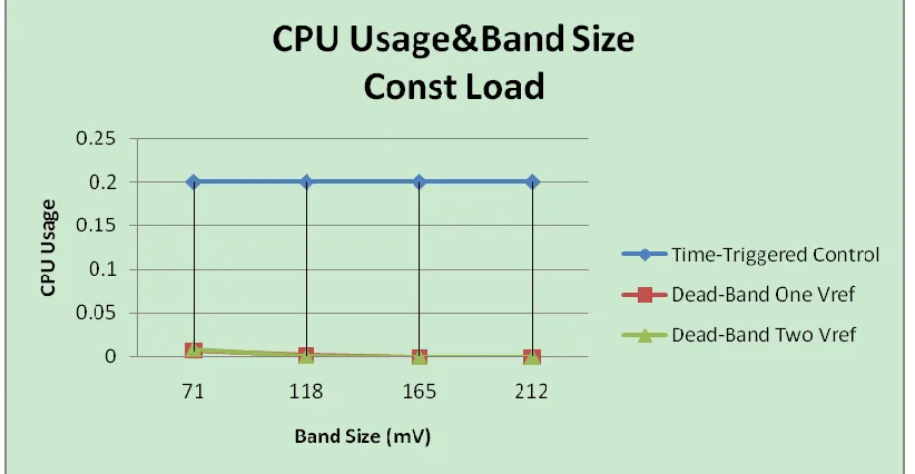
4.3.1 Analysis for Constant Load
Figure 4-21Analysis: CPU usage of constant load
From Figure 4-21, we can see the dead-band control reduces about 90% of CPU utilization
compared with time-triggered control. Dead-band control with two reference voltages has
even less utilization than the other two control modes.
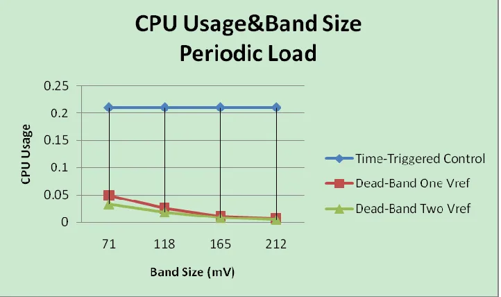
Figure 4-22 Analysis: CPU usage of periodical load
From Figure 4-22, we can see the dead-band control reduces 75% of CPU utilization
compared with time-triggered control. Dead-band control with two reference voltages has
even less utilization than the other two control modes.
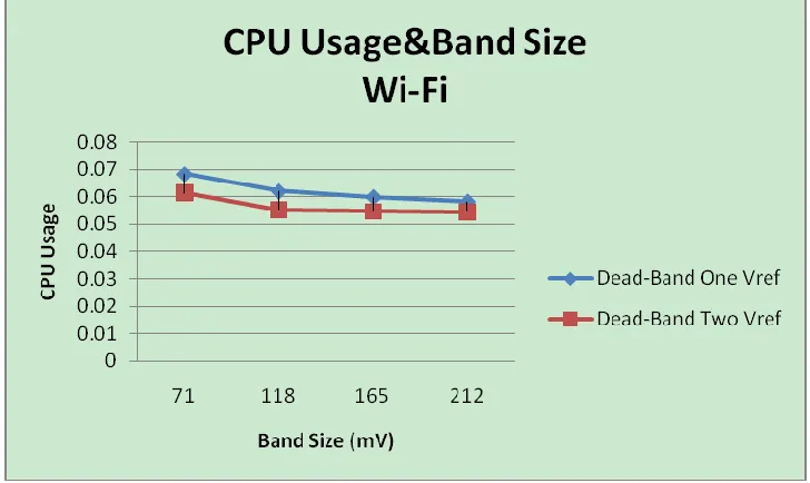
Figure 4-23 Analysis: CPU usage of Wi-Fi module
Because we would like to specifically test dead-band control in Wi-Fi module, we don’t
record the time-triggered control for it. From Figure 4-23, for the two dead-band control
modes, the one with two reference voltages has about 14.28% of CPU utilization lower than
Chapter 5 CONCLUSION AND FUTURE WORK 5.1 Conclusion
In this thesis, I implemented dead-band control, compared the CPU usage between it and
sampling-triggered control. I conclude that dead-band control will reduce the CPU usage
significantly. The amount of reduction depends on the load transient size and frequency,
dead-band size, PI control parameter setting and the number of reference voltages. The
results are based on the overall integrations and relationships among the factors above. The
factors have the following effects on CPU usage.
Increasing dead-band size will potentially result in reduction of CPU usage. However, if the
system has poor PI parameters, the system will oscillate and goes out of the dead-band a lot,
which increases CPU usage. This problem could be solved by using two reference voltages
without changing the PI parameters.
If control signal is large, the output voltage will converge back to reference voltage(s) fast,
which means the system has longer time to be in the dead-band. This will reduce CPU usage.
But it may cause oscillations between two bands. As mentioned below, two reference
voltages could solve this problem, but the system performance will decay and could have
larger steady-state error.
If two reference voltages are used, the control signal is smaller compared with one reference
voltage. If the system is not very stable with one reference voltage, two reference voltages
could stabilize the system and keep the system within the dead-band longer, which reduces
CPU usage. However, two reference voltages method may cause larger steady-state error,
5.2 Future work
The inductor used in the boost converter is 150µH, which makes the system very insensitive
to the control signal. To make the system react to the control signal change faster, a smaller
inductor should be used.
Besides, the current system still has relatively large overshoot. To compensate this overshoot,
feed forward control may be implemented in the future. What’s more, feed forward control
may also lead to a faster control response. [10]
For the code optimization part, the current fixed point number method is hard to understand
to some extent. Which will cause potential maintain problem. To solve this problem,
developing a small tool to convert float point number operation to fixed point number
REFERENCES
[1] Hauke, Brigitte,Texas Instruments, "Basic Calculation of a Boost Converter's Power Stage," Application Report SLVA372C, 2009.
[2] Mitulkumar R. Dave and K. C. Dave, "Analysis of Boost Converter Using PI Control Algorithms," International Journal of Engineering Trands and Technology, vol. 3, no. 2, 2012.
[3] Kiam Heong Ang and Gregory Chong, "PID Control System Analysis, Design, and Technology," IEEE Transactions on Control Systems Technology, vol. 13, no. 4, pp. 559-576, July 2005.
[4] Angel Vladimirov Peterchev and Seth R. Sanders, "Digital Control of PWM Converters: Analysis and," Electrical Engineering and Computer Sciences University of California at Berkeley, Berkeley, Technical Report No. UCB/EECS-2006-146, 2006.
[5] Karl-Erik Årzén, "A Simple Event-Based PID Controller," in IFAC World Congress, 1999.
[6] Sylvain Durand and Nicolas Marchand, "An Event-Based PID Controller With Low Computational Cost," in 8th International Conference on Sampling Theory and Applications, Marseille, 2010.
[7] Sylvain Durand and Nicolas Marchand, "Further Results on Event-Based PID Controller," in European Control Conference, Budapest, 2009.
[8] Nan Xing, Yujuan Lin, and Jinhui Zhang, "Some Improvements on Event-Based PID Controllers," in the 32nd Chinese Control Conference, Xi'an, 2013.
[9] Robert W. Erickson and Dragan Maksimović, Fundamentals of Power Electronics, Second Edition ed. Bouder,Colorado, USA: Kluwer Academic Publishers, 2001.
Appendix A. Waveforms of Dead-Band Control with One Reference Voltage for the
Periodically Changed Load
a. Dead-band: 3.326V to 3.255V
Figure 5-1 Periodical load in dead-band control: one-reference-voltage, dead bands 3.326V to 3.255V, zoom-out version
Figure 5-2 Periodical load in dead-band control: one-reference-voltage, dead bands 3.326V to 3.255V, zoom-in version
Figure 5-3 Periodical load in dead-band control: one-reference-voltage, dead bands 3.350V to 3.232V, zoom-out version
Figure 5-4 Periodical load in dead-band control: one-reference-voltage, dead bands 3.350V to 3.232V, zoom-in version
Figure 5-5 Periodical load in dead-band control: one-reference-voltage, dead bands 3.373V to 3.208V, zoom-out version
Figure 5-6 Periodical load in dead-band control: one-reference-voltage, dead bands 3.373V to 3.208V, zoom-in version
Appendix B. Waveforms of Dead-Band Control with Two Reference Voltages for the
Periodically Changed Load
a. Dead-band: 3.326V to 3.255V
Figure 5-7 Periodical load in dead-band control: two-reference-voltage, dead bands 3.326V to 3.255V, zoom-out version
Figure 5-8 Periodical load in dead-band control: two-reference-voltage, dead bands 3.326V to 3.255V, zoom-in version
Figure 5-9 Periodical load in dead-band control: two-reference-voltage, dead bands 3.350V to 3.232V, zoom-out version
Figure 5-10 Periodical load in dead-band control: two-reference-voltage, dead bands 3.350V to 3.232V, zoom-in version
Figure 5-11 Periodical load in dead-band control: two-reference-voltage, dead bands 3.373V to 3.208V, zoom-out version
Appendix C. Waveforms of Dead-Band Control with One Reference Voltages for the
Constant Load
a. Dead-band: 3.373V to 3.208V
Figure 5-13 Constant load in dead-band control: one-reference-voltage, dead bands 3.373V to 3.208V
b. Dead-band: 3.350V to 3.232V
c. Dead-band: 3.326V to 3.255V
Appendix D. Waveforms of Dead-Band Control with Two Reference Voltages for the
Constant Load
a. Dead-band: 3.373V to 3.208V
Figure 5-16 Constant load in dead-band control: two-reference-voltage, dead bands 3.373V to 3.208V
b. Dead-band: 3.350V to 3.232V
c. Dead-band: 3.326V to 3.255V
Appendix E. Object Code
126 __interrupt static void r_adc_interrupt(void) \ r_adc_interrupt:
127 {
128 /* Start user code. Do not edit comment generated here */ 129 /* Upper byte of the ADCR register holds the ADC result */ 130
131 //signed short delta_TDR01_temp; 132 P4_bit.no1 = 1; // pin 11 on MCU
\ 000000 711204 SET1 S:0xFFF04.1 ;; 2 cycles 133
134 flag_overflow = 0;
\ 000003 F5.... CLRB N:flag_overflow ;; 1 cycle \ 000006 61DF SEL RB1
135 Cpu_CounterT = TCR10;
\ 000008 AFC001 MOVW AX, 0x1C0 ;; 1 cycle \ 00000B BF.... MOVW N:Cpu_CounterT, AX ;; 1 cycle 136 //R_TAU1_Channel0_Start();
137 gADC_Result = ADCR;
\ 00000E AD1E MOVW AX, S:0xFFF1E ;; 1 cycle \ 000010 BF.... MOVW N:gADC_Result, AX ;; 1 cycle 138
139 Voltage_FX = (gADC_Result>>8) + (gADC_Result>>9) + (gADC_Result>>15);
\ 000013 16 MOVW HL, AX ;; 1 cycle \ 000014 31FE SHRW AX, 0xF ;; 1 cycle \ 000016 37 XCHW AX, HL ;; 1 cycle \ 000017 319E SHRW AX, 0x9 ;; 1 cycle \ 000019 14 MOVW DE, AX ;; 1 cycle \ 00001A AF.... MOVW AX, N:gADC_Result ;; 1 cycle \ 00001D F0 CLRB X ;; 1 cycle \ 00001E 08 XCH A, X ;; 1 cycle \ 00001F 05 ADDW AX, DE ;; 1 cycle \ 000020 07 ADDW AX, HL ;; 1 cycle \ 000021 BF.... MOVW N:Voltage_FX, AX ;; 1 cycle 140
141 error_p=error_10_6;
\ 000024 AF.... MOVW AX, N:error_10_6 ;; 1 cycle \ 000027 BF.... MOVW N:error_p, AX ;; 1 cycle 142
143 /*****boost control part******/
144 Mult_R = ((unsigned long)(TDR01_temp)) << 4; //2_14 to 12_20 \ 00002A AF.... MOVW AX, N:TDR01_temp ;; 1 cycle
\ 00002D 16 MOVW HL, AX ;; 1 cycle \ 00002E 31CE SHRW AX, 0xC ;; 1 cycle \ 000030 12 MOVW BC, AX ;; 1 cycle \ 000031 17 MOVW AX, HL ;; 1 cycle \ 000032 314D SHLW AX, 0x4 ;; 1 cycle \ 000034 BF.... MOVW N:Mult_R, AX ;; 1 cycle \ 000037 13 MOVW AX, BC ;; 1 cycle \ 000038 BF.... MOVW N:Mult_R+2, AX ;; 1 cycle 145 //first calculate error_p and K2_boost
146 if(error_flag == 1)
\ 00003B E6 ONEW AX ;; 1 cycle \ 00003C 42.... CMPW AX, N:error_flag ;; 1 cycle \ 00003F DB.... MOVW BC, N:error_p ;; 1 cycle \ 000042 AF.... MOVW AX, N:K2_boost ;; 1 cycle \ 000045 DF13 BNZ ??Handle_Switch_0 ;; 4 cycles \ 000047 ; --- Block: 38 cycles
\ 000047 ; * Stack frame (at entry) * \ 000047 ; Param size: 0
148 Mult_R += K2_boost * error_p;
\ 000047 CEFB01 MULHU ;; 2 cycles \ 00004A EB.... MOVW DE, N:Mult_R ;; 1 cycle \ 00004D F7 CLRW BC ;; 1 cycle \ 00004E 05 ADDW AX, DE ;; 1 cycle \ 00004F 61D8 SKNC
\ 000051 A3 INCW BC ;; 5 cycles \ 000052 FB.... MOVW HL, N:Mult_R+2 ;; 1 cycle \ 000055 33 XCHW AX, BC ;; 1 cycle \ 000056 07 ADDW AX, HL ;; 1 cycle \ 000057 33 XCHW AX, BC ;; 1 cycle \ 000058 EF0E BR S:??Handle_Switch_1 ;; 3 cycles \ 00005A ; --- Block: 17 cycles
149 } 150 else
151 Mult_R -= K2_boost * error_p; \ ??Handle_Switch_0:
\ 00005A CEFB01 MULHU ;; 2 cycles \ 00005D 14 MOVW DE, AX ;; 1 cycle \ 00005E AF.... MOVW AX, N:Mult_R ;; 1 cycle \ 000061 DB.... MOVW BC, N:Mult_R+2 ;; 1 cycle \ 000064 25 SUBW AX, DE ;; 1 cycle \ 000065 61D8 SKNC
\ 000067 B3 DECW BC ;; 5 cycles \ 000068 ; --- Block: 11 cycles
\ ??Handle_Switch_1:
\ 000068 BF.... MOVW N:Mult_R, AX ;; 1 cycle \ 00006B 13 MOVW AX, BC ;; 1 cycle \ 00006C BF.... MOVW N:Mult_R+2, AX ;; 1 cycle 152
153 if(One_Vref){
\ 00006F D5.... CMP0 N:One_Vref ;; 1 cycle \ 000072 DD5C BZ ??Handle_Switch_2 ;; 4 cycles \ 000074 ; --- Block: 8 cycles
154 //then calculate error_10_6 and K1 boosst 155 if(Vref <= Voltage_FX)
\ 000074 FB.... MOVW HL, N:Vref ;; 1 cycle \ 000077 AF.... MOVW AX, N:Voltage_FX ;; 1 cycle \ 00007A 47 CMPW AX, HL ;; 1 cycle \ 00007B DC21 BC ??Handle_Switch_3 ;; 4 cycles \ 00007D ; --- Block: 7 cycles
156 {
157 error_flag = 1;
\ 00007D E6 ONEW AX ;; 1 cycle \ 00007E BF.... MOVW N:error_flag, AX ;; 1 cycle 158 error_10_6 = Voltage_FX - Vref;
\ 000081 AF.... MOVW AX, N:Voltage_FX ;; 1 cycle \ 000084 22.... SUBW AX, N:Vref ;; 1 cycle \ 000087 BF.... MOVW N:error_10_6, AX ;; 1 cycle 159 Mult_R -= K1_boost * error_10_6;
\ 00008A 12 MOVW BC, AX ;; 1 cycle \ 00008B AF.... MOVW AX, N:K1_boost ;; 1 cycle \ 00008E CEFB01 MULHU ;; 2 cycles \ 000091 14 MOVW DE, AX ;; 1 cycle \ 000092 AF.... MOVW AX, N:Mult_R ;; 1 cycle \ 000095 DB.... MOVW BC, N:Mult_R+2 ;; 1 cycle \ 000098 25 SUBW AX, DE ;; 1 cycle \ 000099 61D8 SKNC
\ 00009E ; --- Block: 21 cycles
160 }
161 else if(Vref >= Voltage_FX) \ ??Handle_Switch_3:
\ 00009E FB.... MOVW HL, N:Voltage_FX ;; 1 cycle \ 0000A1 AF.... MOVW AX, N:Vref ;; 1 cycle \ 0000A4 47 CMPW AX, HL ;; 1 cycle \ 0000A5 DC29 BC ??Handle_Switch_2 ;; 4 cycles \ 0000A7 ; --- Block: 7 cycles
162 {
163 error_flag = 0;
\ 0000A7 F6 CLRW AX ;; 1 cycle \ 0000A8 BF.... MOVW N:error_flag, AX ;; 1 cycle 164 error_10_6 = Vref - Voltage_FX;
\ 0000AB AF.... MOVW AX, N:Vref ;; 1 cycle \ 0000AE 22.... SUBW AX, N:Voltage_FX ;; 1 cycle \ 0000B1 BF.... MOVW N:error_10_6, AX ;; 1 cycle 165 Mult_R += K1_boost * error_10_6;
\ 0000B4 12 MOVW BC, AX ;; 1 cycle \ 0000B5 AF.... MOVW AX, N:K1_boost ;; 1 cycle \ 0000B8 CEFB01 MULHU ;; 2 cycles \ 0000BB EB.... MOVW DE, N:Mult_R ;; 1 cycle \ 0000BE F7 CLRW BC ;; 1 cycle \ 0000BF 05 ADDW AX, DE ;; 1 cycle \ 0000C0 61D8 SKNC
\ 0000C2 A3 INCW BC ;; 5 cycles \ 0000C3 FB.... MOVW HL, N:Mult_R+2 ;; 1 cycle \ 0000C6 33 XCHW AX, BC ;; 1 cycle \ 0000C7 07 ADDW AX, HL ;; 1 cycle \ 0000C8 33 XCHW AX, BC ;; 1 cycle
\ 0000C9 ; --- Block: 21 cycles
\ ??Handle_Switch_4:
\ 0000C9 BF.... MOVW N:Mult_R, AX ;; 1 cycle \ 0000CC 13 MOVW AX, BC ;; 1 cycle \ 0000CD BF.... MOVW N:Mult_R+2, AX ;; 1 cycle
\ 0000D0 ; --- Block: 3 cycles
166 167 } 168 }
169 if(Two_Vref){
\ ??Handle_Switch_2:
\ 0000D0 D5.... CMP0 N:Two_Vref ;; 1 cycle \ 0000D3 DD5C BZ ??Handle_Switch_5 ;; 4 cycles \ 0000D5 ; --- Block: 5 cycles
170 //then calculate error_10_6 and K1 boosst 171 if(Vrefu <= Voltage_FX)
\ 0000D5 FB.... MOVW HL, N:Vrefu ;; 1 cycle \ 0000D8 AF.... MOVW AX, N:Voltage_FX ;; 1 cycle \ 0000DB 47 CMPW AX, HL ;; 1 cycle \ 0000DC DC21 BC ??Handle_Switch_6 ;; 4 cycles \ 0000DE ; --- Block: 7 cycles
172 {
173 error_flag = 1;
\ 0000DE E6 ONEW AX ;; 1 cycle \ 0000DF BF.... MOVW N:error_flag, AX ;; 1 cycle 174 error_10_6 = Voltage_FX - Vrefu;
175 Mult_R -= K1_boost * error_10_6;
\ 0000EB 12 MOVW BC, AX ;; 1 cycle \ 0000EC AF.... MOVW AX, N:K1_boost ;; 1 cycle \ 0000EF CEFB01 MULHU ;; 2 cycles \ 0000F2 14 MOVW DE, AX ;; 1 cycle \ 0000F3 AF.... MOVW AX, N:Mult_R ;; 1 cycle \ 0000F6 DB.... MOVW BC, N:Mult_R+2 ;; 1 cycle \ 0000F9 25 SUBW AX, DE ;; 1 cycle \ 0000FA 61D8 SKNC
\ 0000FC B3 DECW BC ;; 5 cycles \ 0000FD EF2B BR S:??Handle_Switch_7 ;; 3 cycles \ 0000FF ; --- Block: 21 cycles
176 }
177 else if(Vrefl >= Voltage_FX) \ ??Handle_Switch_6:
\ 0000FF FB.... MOVW HL, N:Voltage_FX ;; 1 cycle \ 000102 AF.... MOVW AX, N:Vrefl ;; 1 cycle \ 000105 47 CMPW AX, HL ;; 1 cycle \ 000106 DC29 BC ??Handle_Switch_5 ;; 4 cycles \ 000108 ; --- Block: 7 cycles
178 {
179 error_flag = 0;
\ 000108 F6 CLRW AX ;; 1 cycle \ 000109 BF.... MOVW N:error_flag, AX ;; 1 cycle 180 error_10_6 = Vrefl - Voltage_FX;
\ 00010C AF.... MOVW AX, N:Vrefl ;; 1 cycle \ 00010F 22.... SUBW AX, N:Voltage_FX ;; 1 cycle \ 000112 BF.... MOVW N:error_10_6, AX ;; 1 cycle 181 Mult_R += K1_boost * error_10_6;
\ 000115 12 MOVW BC, AX ;; 1 cycle \ 000116 AF.... MOVW AX, N:K1_boost ;; 1 cycle \ 000119 CEFB01 MULHU ;; 2 cycles \ 00011C EB.... MOVW DE, N:Mult_R ;; 1 cycle \ 00011F F7 CLRW BC ;; 1 cycle \ 000120 05 ADDW AX, DE ;; 1 cycle \ 000121 61D8 SKNC
\ 000123 A3 INCW BC ;; 5 cycles \ 000124 FB.... MOVW HL, N:Mult_R+2 ;; 1 cycle \ 000127 33 XCHW AX, BC ;; 1 cycle \ 000128 07 ADDW AX, HL ;; 1 cycle \ 000129 33 XCHW AX, BC ;; 1 cycle
\ 00012A ; --- Block: 21 cycles
\ ??Handle_Switch_7:
\ 00012A BF.... MOVW N:Mult_R, AX ;; 1 cycle \ 00012D 13 MOVW AX, BC ;; 1 cycle \ 00012E BF.... MOVW N:Mult_R+2, AX ;; 1 cycle
\ 000131 ; --- Block: 3 cycles
182 183 } 184 }
185 // normalize MAC accumulator from 12-20 down to 2-14 186 TDR01_temp = (unsigned short)(Mult_R >> 4);
\ ??Handle_Switch_5:
\ 000131 AF.... MOVW AX, N:Mult_R ;; 1 cycle \ 000134 DB.... MOVW BC, N:Mult_R+2 ;; 1 cycle \ 000137 314E SHRW AX, 0x4 ;; 1 cycle \ 000139 33 XCHW AX, BC ;; 1 cycle \ 00013A 31CD SHLW AX, 0xC ;; 1 cycle \ 00013C 03 ADDW AX, BC ;; 1 cycle 187 /******duty cycle restraints****/