Design of Four Element Array based Antenna with
Defected Ground Structure to improve Gain and
Return loss
Nitin Sharma1, Jyoti2
1
Mtech Student, Electronics and Communication Department,SUS College of Engineering and Technology, Tangori, Mohali, Punjab, India
2
Assistant Professor, Electronics and Communication Department,SUS College of Engineering and Technology, Tangori, Mohali, Punjab, India
Abstract
In this paper a four element antenna for GSM applications has been proposed. The elements can be fed by a single line or by multiple lines in a feed network arrangement,so we have proposed an array to improve the performance of wireless antenna. In this work, concept of defected ground structure has also been proposed to achieve greater bandwidth of microstrip patch antenna. The basic element of DGS is a resonant gap or slot in the ground metal, placed directly under a transmission line and aligned for efficient coupling to the line. The proposed antenna array will be designed in various design stages. First,A single antenna without defected ground structure will be designed and simulated as well.Then Same antenna using same feeding method and same dielectric constant will be designed with defected ground structure. At the third stage, antenna designed at second stage will be converted in to antenna array. At the final and last stage, results obtained from all the previous design stages will be compared. The proposed antenna will be designed using perfect electric conducting material on Roggers RT5880 substrate having 2.2 dielectric constant. The proposed antenna will be designed using user friendly CST Microwave studio Software.
Keywords: Antenna Array, Defected Ground Structure (DGS), CST Microwave Studio .
1. Introduction
Antennas play a very important role in the field of wireless communications. Some of them are parabolic reflectors, patch antennas, slot antennas and folded dipole antennas. Each type of antenna is good in its own properties and usage. We can say antennas are the backbone and almost everything in the wireless communication without which the word could have not reached at this age of technology. Patch antennas play a
very significant role in today's world of wireless communication systems. A microstrip patch antenna is very simple in the construction using a conventional microstrip fabrication technique. The patch can take any shape but rectangular and circular configurations are the most commonly used configurations.
To synthesize a required radiation pattern with improved return loss that cannot be achieved with a single element, In this dissertation work a four element antenna for GSM applications has been proposed. The elements can be fed by a single line or by multiple lines in a feed network arrangement, so in this dissertation work, we have also proposed an array to improve the performance of wireless antenna. Antenna is one of the important element in RF system in transmitting and receiving signal from and into air as medium. In order to simplify analysis and performance prediction, the patch is generally square, rectangular, circular, triangular, and elliptical or some other common shape. Modern wireless communication system requires low profile, light weight, high gain, and simple structure antennas to assure reliability, mobility, and high efficiency characteristics [1]. These advantages of microstrip antennas make them popular in many wireless communication applications such as telemetry and
communications, aviation, naval communications,
over the air or by propagating surface currents through the ground plane. Surface currents can be a bigger problem, especially when antenna elements are closely packed. Microstrip patch antennas are well-known antenna types .In general, the structure has a thin metallic patch, usually copper, printed on a microwave substrate. There are many methods for reducing the effects of mutual coupling, which include optimizing antenna dimensions, grooving the dielectric, covering the patch by additional dielectric layers, using shorting pins to cancel the capacitive polarization currents of the substrate, adding parasitic conducting tape to the middle of two antennas , using the dielectric as a band gap structure between elements in the array, or using Defected Ground Structures (DGSs) technique which are widely used in microwave circuit and antenna design because they produce the band rejection characteristics similar to EBG structures but with a more compact size[6].
The proposed antenna array will be designed in various design stages. First,A single antenna without defected ground structure will be designed and simulated as well.Then Same antenna using same feeding method and same dielectric constant will be designed with defected ground structure. At the third stage, antenna designed at second stage will be converted in to antenna array. At the final and last stage, results obtained from all the previous design stages will be compared.
2. First Stage of Antenna Design
In the first of stage of dissertation work, first we designed a simple microstrip patch antenna. The three essential parameters for the design of a rectangular microstrip patch antenna using traditional method are:
(i) Frequency of operation (fo ):
The resonant frequency of the antenna must be selected appropriately. The resonant frequency selected for design is at 2.4 GHz.
(ii) Dielectric constant of the substrate (Er):
The dielectric material selected for the design is Rogers RT5880 which has a dielectric constant of 2.2. A substrate with a high dielectric constant reduces the dimensions of the antenna.
(iii) Height of dielectric substrate (h):
For the microstrip patch antenna it is essential that the antenna is not bulky. Hence, the height of the dielectric substrate is selected as 0.78 mm.
The design parameters that are assumed and evaluated are shown in Fig.1 as below:
Figure1: Perspective view of Microstrip Patch Antenna
By using above essential parameters ,first we calculated all the required antenna specifications.After this antenna was designed and optimization was done using CST Microwave Studio 2010.Optimized values of the designed antenna are given in the following table .
Sr. No.
Parameter Name Optimized Values
1. Length of Patch (Lp) 41 mm
2. Width of Patch (Wp) 49 mm
3. Length of Ground (Lg) 47 mm
4. Width of Ground (Wg) 54 mm
5. Width of Feed (Wf) 1.79 mm
6. Dielectric Constant (Er) 2.2
7. Height of Substrate(h) 0.78 mm
3. Second Stage of Antenna Design
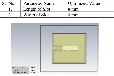
In the second stage, We Introduced the concept of defected ground structure (DGS).Here we cut a slot in ground sheet. Optimization was done in order to improve return loss of antenna.Otimized values of Slot are given as below. Defected ground structure is shown below.
Sr. No. Parameter Name Optimized Value
1. Length of Slot 8 mm
2. Width of Slot 4 mm
4. Final Stage: Design of Antenna Array
In this stage of antenna design 1*4 elements array is designed .Here, a single microstrip line feed is used for 4 element antenna array. Following figure shows the structure of 4 element antenna array.
Figure 3: Four Element antenna Array
5. Results and Discussion
Figure 4:Return Loss of microstrip patch antenna
Figure 5:Return Loss of 4 Element Antenna Array with Defected Ground
Figure 5 shows the the return loss of microstrip patch four element array with defected ground.As you can see here due to defected ground and array return loss has been improved a lot. Antenna Array with defected ground brought about 58% improvement in results of antenna.Gain of both the designs remain almost same.We used a single feed line to give excitation signal at the input of antenna.
Figure 6 shows the 3D pattern of directivity of antenna.Simple microstrip patch antenna gives optimum Gain of 6.8 dB.As we can observe from the figure that antenna is highly directive and it radiates properly in one direction as compare to other one.[7]-[12]
Figure 7 shows the 3D directivity pattern of four element antenna array with defected ground.As we observed here that gain of array is 9.0 dB which is far better than the gain of simple microstrip patch. Antenna array improved more than 30% gain of the design
Figure 7:Direcivity/Gain Pattern of four Element antenna Array
Figure 8:VSWR Plot of Microstrip Patch antenna
Figure 8 shows the VSWR of the microstrip patch antenna.Ideal value of VSWR is 1 and practical value of VSWR should be lesser than 2.AS we can observe from figure that VSWR of microstrip patch antenna is 1.2Which means that maximum input signal is transferred to the output.Figure 9 shows VSWR plot of four element array.Here we can observe value is 1.1 which is better than the VSWR of the microstrip patch antenna.
Figure 9: VSWR Plot of Four Element An
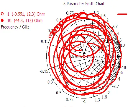
Figure 9 and 10 shows the smith chart of simple microstrip patch antenna and four element antenna array respectively. In this proposed work, input impedance is perfectly matched without using any external device. Input impedance is matched by varying the width of line feed.Input impedance is inversely proportional to the width of line feed. Ideally and practically value of input
impedance is 50 Ohms.
Figure 10: Smith Chart of four Element Array
6. Conclusion
In this proposed work, we designed four element array based antenna with defected ground structure.The whole work was carried out in three stages.In the first stage we designed simple microstrip patch antenna. Geometrical dimensions of the antenna were optimized to have optimum values for Simple microstrip patch .Optimized values for all the dimensions are given in Table 1.Designed
antenna is having -23 dB return loss,6.8 dB
directivity/Gain,50 Ohms input impedanoce and VSWR-1.2 .After this we designed a defected ground structure by introducing a slot in the ground plane.Dimensions of the slot are given in Table 2.In the final stage of work,we designed four element array based antenna.Here we used single microstrip line feed to give input signal to antenna.All the resultant values of simple microstrip patch antenna were compared with the resultant values of Four element antenna array.After comparison we found that
antenna performance was improved to a great
extent.Antenna Array is having -38 dB return loss,9.0 dB Gain,VSWR-1.1,input impedance of 50 ohms.Overall antenna array performance is more than 50 % better than the simple microstrip patch antenna.The designed microstrip antenna array can be used for GSM applications.
References
[1] C. A. Balanis, “AntennaTheory” JohnWiley & Sons, 3rd edition, 2005 chp-4 pp.
722-784
[2] H Singh, “Electromagnetics and Antennas”, Katson publication, New Delhi, 2nd edition.
[3] Ashwini Kumar Arya., A. Patnaik, ,” Defected Ground Structure in the perspective of Microstrip Antennas: A Review, June
[4] K. S. Ahmad1, 2, S. A. Hamzah F., “defected ground structure for beam steering array Antenna applications”Oct 2015.
[5] Chan Hwang See and Khalid G Samarah “A Printed Wideband MIMO Antenna for Mobile and Portable Communication Devices”, APACE 2003. Asia-Pacific Conference on Applied Electromagnetics, pp: 38 – 41, 2003. [6] Guang-ming Zhang,Hong-jing Song,Bing-zhong Wang, Qin-ying Qin,” A Novel dual-band microstrip antenna for WLAN Applications”, IET International Communication Conference on Wireless Mobile and Computing, pp:269-271, 2010. [7] Raghava N.S. De A., Arora P. , Malhotra S. ,Bazaz, R. ;
Kapur S. , Manocha R.,“A Novel Patch Antenna for Ultra Wideband Applications”, International Conference on Communications and Signal Processing (ICCSP), pp:276-279, 2011.
[8] Taheri M.M.S., Hassani H.R., Nezhad S.M.A., “UWB Printed Slot Antenna With Bluetooth and Dual Notch Bands”, IEEE Antennas and Wireless Propagation Letters, Vol-10, pp: 255-258, 2010,
[9] Parmar Kapil and Kumari Runa and Behera S K, “M-Shaped dielectric resonator antenna for WLAN applications”, International Conference on Devices and Communications (ICDeCom), pp-1-4, 2011.
[10] Nguyen T. D., Lee D. H., Park H. C., “Design and Analysis of Compact Printed Triple Band-Notched UWB Antenna” IEEE Antennas and Wireless Propagation Letters, pp-403, 2011.