Design and Simulation of 64-Bit Carry Select
Adder Using Gate Level Architecture for Low
Power Applications
Rohit Khare
1, Sandip Nemade
2M. Tech., Dept. of ECE, TIT, RGTU Bhopal, Madhya Pradesh, India1
Assistant Professor [VLSI], Dept. of ECE, TIT, RGTU Bhopal, Madhya Pradesh, India2
ABSTRACT: An efficient VLSI based system has a very high speed operation capability along with low power
requirement for performing any operation. The modern systems are required to have very efficient hardware architecture in order to utilize the hardware efficiency to result in best performance. The increasing processor speed and data handling require a high speed circuit to perform the complex calculations. The basic processing operations include addition, multiplication, division, code conversion, encoding-decoding, encryption-decryption, mixing of signal, register-shift, etc. These operations are performed in combination to result in a complex operation. Addition is among the simplest operations. For a data with high length the time taken by the adder to generate output increases in proportion to the length of data. The present work presents the design and simulation of gate level circuit of a 64-bit carry select adder (CSLA) design. The design of CSLA and its simulation test-bench is written using VHDL language. This brief also presents an analysis based on the dynamic power consumption of the field programmable gate array (FPGA) devices in performing the addition operation using the presented design. Xilinx Tool is used in performing the design, simulation and synthesis of the present work.
KEYWORDS: VLSI, FPGA, CSLA, Dynamic Power, Xilinx.
I. INTRODUCTION
In the present scenario of low power system design using VLSI technology, high speed is the main parameter that needs the attention by the researchers to meet the emerging requirement of such systems to handle the data processing functionality. The efficiency of a system can be improved by many focussed improvements in the intermittent logics. In the digital signal processor (DSP) based architecture; high speed arithmetic logic operations play a very important role in giving high speed to the processor. Arithmetic addition for a long-length data size is a time consuming operation. The multiple bit addition is a serial operation since in the arithmetic addition two binary numbers the corresponding bit addition results in the carry bit generation that is transferred to the next bit addition. So, a data with a long length takes comparatively longer time as compared to the time taken for the addition of comparatively shorter length data. The propagation of carry bit through the complete data length is the main time requiring operation that adds delay to the addition operation. And since the addition operation is one of the most basic operation in signal processing, so its delay is reflected in the complete processing operation. A highly synchronized logic require the minimum skew time in the circuits that operate on clock edge. For the circuits that are time optimized and synchronous a novel architecture of adder is preferred that fulfil the timing constraint of the circuit. Researchers and designers has proposed a number of adder architectures, like Ripple Carry Adder, Carry Skip Adder, Carry Save Adder, Carry Look Ahead Adder and Carry Sect Adder. The present work is focussed on the architectural design and implementation of Carry Select Adder.
II. LITERATURE REVIEW
area. A power-area efficient gate level modified design is implemented in [15, 4, 8] by minimizing the logic operation in comparison with the conventional CSLA design. Analysis of 16-bit conventional CSLA and Binary to Excess-1 Converter (BEC) CSLA is presented in [7] and a D-latch based CSLA architecture is proposed in this paper. An area-delay optimized architecture of 16-bit, 32-bit and 64-bit CSLA adder is proposed and analyzed in [5, 6]. Reference [16] presents simulation and performance evaluation of a 16-bit modified architecture of Square-Root CSLA (SQRT-CSLA). Area-Delay-Power based simulation of redundant logic optimized modified design of CSLA with respect to the conventional CSLA design is shown in [9, 10, 11, 12]. A modified design for 16-bit, 32-bit and 64-bit CSLA is proposed in [19] that does not uses multiplexer architecture. This paper also shows a comparative analysis of the proposed architecture with the conventional architecture. A logic converter unit (LCU) based modified architecture of adder is proposed in [20] for optimized area-delay-power parameter. The modified architectures find applications in high performance VLSI system architectures in the development of modern electronic devices and gadgets. An efficient architecture of Adder essentially improves the overall performance of complex systems. The different sections of the proposed work are arranged as: Section II presents the architecture of 64-bit CSLA and the design of its building block using gate level logic. Section III presents the simulation and synthesis results. This section also shows the comparative analysis of the design for dynamic power consumption on different FPGAs. Section IV presents the conclusion based on the present design simulation analysis. In the last, this paper is concluded with the acknowledgement and the references.
III. ARCHITECTURE OF CARRY SELECT ADDER 64-BIT
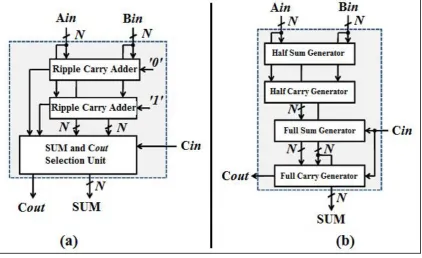
In the conventional adder design using ripple carry adder as the basic building block, as shown in fig 1(a), there are two ripple carry adders (RCA) and a SUM and Carry Selection Unit (SCU). Most of the logic resources of the CSLA are present in the SCU. This logic unit also contributes to the critical path of the adder logic. For an „N‟-bit adder, two N-bit RCAs are used. A typical logic block diagram of RCA is shown in fig 1(b).
Fig. 1 Logic Block Diagram of:
(a) Conventional Carry Selector Unit, and (b) Ripple Carry Adder
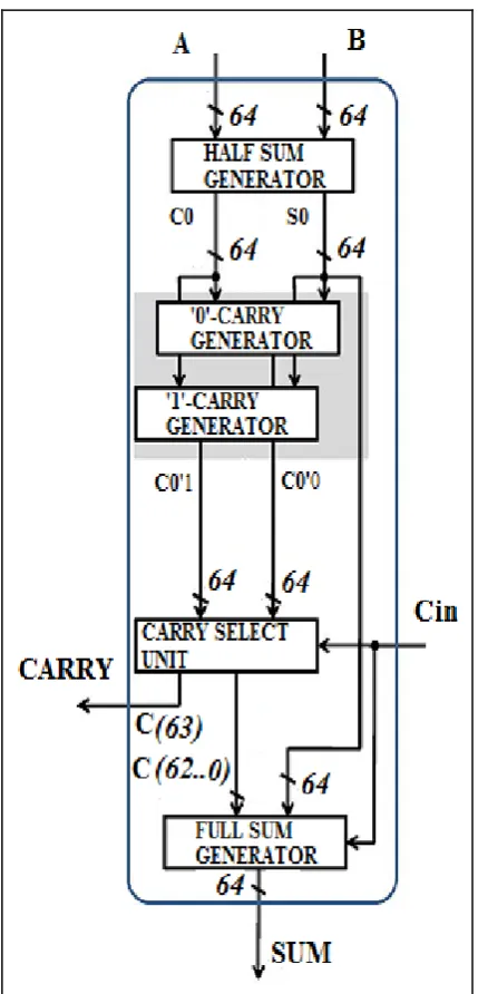
using the conventional half adder circuit using the corresponding bits of the CSLA. It consists of N numbers of XOR-gates and AND-XOR-gates to perform the operation.
Fig. 2 Logic Block Flow Diagram of Carry Select Adder
computational time in the CSLA design. The CSU unit selects the carry as per the carry input of the CSLA. The MSB output of CSU block is the carry output of the CSLA operation. The FSG block generates the sum bits of the CSLA operation by adding the sum output from the HSG block and the carry outputs of the CSU block.
Fig. 3 Gate level logics of Internal Blocks of „N‟-bit CSLA
Table I: Number of Logic Gates in 64-bit CSLA Design Blocks
CSA Block AND Gate OR Gate XOR Gate
HSG 64 - 64
CG0 63 63 -
CG1 63 64 -
CSU 64 64 -
FSG - - 64
Total 254 191 128
Table II: Number of Logic Gates in 16-bit, 32-bit and 64-bit CSLA Design
CSA Design AND Gate OR Gate XOR Gate
16-bit 62 47 32
32-bit 126 95 64
64-bit 254 191 128
Table I specifies the number of AND, OR and XOR logic gates that are used to design the gate level architecture of the internal blocks of 64-bit CSLA in the present work. A comparative gates requirement of design of 16-bit, 32-bit and 64-bit CSLA design is shown in Table II.
IV. RESULT AND DISCUSSION
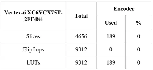
The design is simulated for functional verification and dynamic power consumption. Xilinx ISE Tool is used for performing functional and power simulation. Table III shows the resource utilization summary of the carry select adder design for Vertex-6 XC6VCX75T-2FF484 FPGA. Since the operation is a combinational execution so no flipflops are required to store any intermediate value of processing data.
Table III: Hardware Utilization Summary of Proposed CSLA Design
Vertex-6
XC6VCX75T-2FF484 Total
Encoder
Used %
Slices 4656 189 0
Flipflops 9312 0 0
LUTs 9312 189 0
Table IV: Frequency Vs. Power Analysis at Different Voltage
Device
Device Voltage
Freq. MHz
Power (W)
VCCaux VCCint Dynamic Total
XC6SLX150-2FGG900 2.5 V 1.2 V
500 0.218 0.339 300 0.131 0.249 100 0.044 0.158
XC6VCX75T-2FF484 2.5 V 1.0 V
500 0.165 1.462 300 0.099 1.394 100 0.033 1.327
XC7K70T-2LFBG676 1.8 V 1.0 V
500 0.134 0.242 300 0.081 0.188 100 0.027 0.135
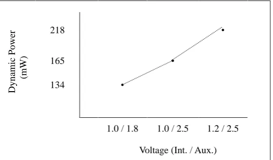
Fig 4 shows the comparative dynamic power variation of the proposed Carry Select Adder design at a constant frequency of 500 MHz against the chip voltages for the mentioned FPGA devices. This analysis shows that the Kintex-7 family device gives the best power performance among these devices. The Kintex Family device that is used to simulate power consumption of the proposed design has an international voltage 1.0V and auxiliary voltage 1.8V. Table IV presents a comparative dynamic power consumption of the implemented design on FPGAs with different operational voltages. Dy n am ic Po w er (m W )
218 •
165 •
134 •
1.0 / 1.8 1.0 / 2.5 1.2 / 2.5
Voltage (Int. / Aux.)
Fig. 4 Frequency Versus Dynamic Power variation of proposed design for Kintex-7 Family FPGA Device
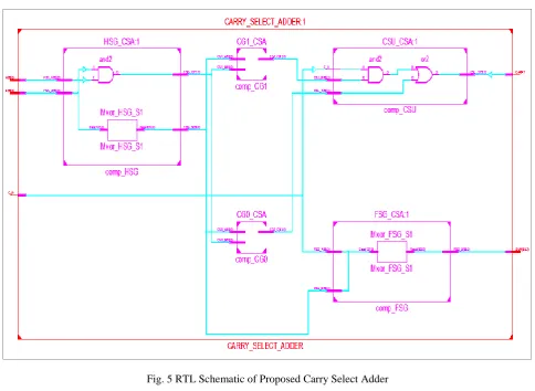
Fig. 5 RTL Schematic of Proposed Carry Select Adder
Fig. 6 Waveform Simulation of Carry Select Adder.
V. CONCLUSION
processing applications that require addition operation hardware. In future the multiplier and the test pattern generator can be configured to match the application specific requirement of the design for a BIST based hardware design implementation. The present work also has the scope of combining other existing hardware designs with this design for a complex logic implementation.
REFERENCES
1. Basant Kumar Mohanty and Sujit Kumar Patel, “Area Delay Power Efficient Carry Select Adder”, IEEE Transactions on Circuits and Systems-II, Volume-61 No.-6, 2014.
2. Gurpreet Kaur, Loveleen Kaur and Navdeep Kaur, “Reduced Area Carry Select Adder with Low Power Consumptions”, International Journal of Emerging Engineering Research and Technology, Volume-3 Issue-3, 2015.
3. S. A. Mashankar, R. D. Kadam and P. R. Indurkar, “Power Efficient Carry Select Adder using D-Latch” International Research Journal of Engineering and Technology, Volume-2 Issue-3, 2015.
4. M. D. Bobade and m. n. Kakatkar, “Implementation on FPGA Area-Delay Efficient Architecture of CSLA” International Journal of Advanced Research in Electrical, Electronics and Instrumentation Engineering, Volume-4 Issue-6, 2015.
5. Priya H. Agrawal and Prashant R. Rothe, “Implementation of Area Delay and Power Efficient Carry Select Adder”, International Journal of Innovative Research in Electrical, Electronics, Instrumentation and Control Engineering, Volume-3 Issue-7, 2015.
6. Theegala Ravinder Reddy and P. Anjaiah, “Design of High Speed Hybrid Carry Select Adder”, International Journal and Magazine of Engineering, Technology, Management and Research, Volume-2 Issue-7, 2015.
7. Lingappagari Raju and Tipparti Anil Kumar, “FPGA Implementation of Efficient Carry-Select-Adder using Verilog HDL”, International Journal and Magazine of Engineering, Technology, Management and Research, Volume-2 Issue-6, 2015.
8. Korra Ravi Kumar, Santosh Kumar Allenki and G. Ramesh, “FPGA Implementation of Area Delay and Power Efficient Carry Select Adder Architecture Design”, International Journal on Recent and Innovation Trends in Computing and Communication, Volume-3 Issue-5, 2015. 9. Anna Johnson and Rakesh S., “High Speed Non-Linear CSA used in Wallace Tree Multiplier and in Radix-4 Booth Recorded Multiplier”,
International Journal of Innovative Science, Engineering and Technology, Volume-2 Issue-3, 2015.
10. S. Banu Priya and G. Lingeswaran, “Area Delay Power Efficient and Implementation of Modified Square-Root Carry Select Adder Architecture”, International Journal for Trends in Engineering and Technology, Volume-4 Issue-2, 2015.
11. Priya Meshram, Mithilesh Mahendra and Parag Jawarkar, “Designed Implementation of Modified Area Efficient Enhanced Square-Root Carry Select Adder”, International Journal for Research in Emerging Science and Technology, Volume-2 Issue-5, 2015.
12. S. Murugeswari and S. Kaja Mohideen, “Design of optimized Low-Power and Area-Efficient Digital FIR Filter using Modified Group Structures based Square-Root Carry Select Adder”, Research Journal of Applied Sciences, Engineering and Technology, 2015.
13. Priya H. Agrawal and Prashant R. Rothe, “Implementation of Fast Low-Power and Area Efficient Carry Select Adder”, International Journal on Recent and Innovation Trends in Computing and Communication, Volume-3 Issue-4, 2015.
14. Deepak Kumar Patel, Raksha Chouksey and Minal Saxena, “An Efficient VLSI Architecture for Carry Select Adder without Multiplexer”, International Journal of Computer Applications, Volume-127 No.-9, 2015.