University of Windsor University of Windsor
Scholarship at UWindsor
Scholarship at UWindsor
Electronic Theses and Dissertations Theses, Dissertations, and Major Papers
2012
Characterization of a CMUT Array
Characterization of a CMUT Array
Tugrul Zure
University of Windsor
Follow this and additional works at: https://scholar.uwindsor.ca/etd
Recommended Citation Recommended Citation
Zure, Tugrul, "Characterization of a CMUT Array" (2012). Electronic Theses and Dissertations. 150.
https://scholar.uwindsor.ca/etd/150
Characterization of a CMUT Array
by
Tugrul Zure
A Thesis
Submitted to the Faculty of Graduate Studies through Electrical and Computer Engineering in Partial Fulfillment of the Requirements for
the Degree of Master of Science at the University of Windsor
Windsor, Ontario, Canada
2011
Characterization of a CMUT Array
by
Tugrul Zure
APPROVED BY:
______________________________________________ Dr. Elena Maeva
Department of Physics
______________________________________________ Dr. Roberto Muscedere
Department of Electrical and Computer Engineering
______________________________________________ Dr. Sazzadur Chowdhury, Advisor
Department of Electrical and Computer Engineering
______________________________________________ Dr. Rashid Rashidzadeh, Chair of Defense
DECLARATION OF ORIGINALITY
I hereby certify that I am the sole author of this thesis and that no part of this thesis has been published or submitted for publication.
I certify that, to the best of my knowledge, my thesis does not infringe upon anyone‟s copyright nor violate any proprietary rights and that any ideas, techniques,
quotations, or any other material from the work of other people included in my thesis, published or otherwise, are fully acknowledged in accordance with the standard referencing practices. Furthermore, to the extent that I have included copyrighted material that surpasses the bounds of fair dealing within the meaning of the Canada Copyright Act, I certify that I have obtained a written permission from the copyright owner(s) to include such material(s) in my thesis and have included copies of such copyright clearances to my appendix.
ABSTRACT
Ultrasound transducers are used in a broad range of applications covering from underwater communications to medical imaging and treatment. The ultrasonic transducer determines the key specifications such as resolution, sensitivity and signal to noise ratio. The capacitive micromachined ultrasonic transducer (CMUT) has emerged as an alternative to standard piezoelectric transducers due to advanced microelectronics fabrication technology and methods. Comparing to piezoelectric transducers, the CMUT is superior to it‟s competitor with higher acoustic bandwidth, higher sensitivity and greater coupling with the acoustic medium. Design, fabrication, and characterization of a capacitive micromachined ultrasonic transducer (CMUT) array have been presented along this thesis. The array is designed to operate in the frequency range of 113-167 kHz. The CMUT array is fabricated using an SOI based fabrication technology and includes 6x6 CMUTs. Necessary test setups and readout circuitry is designed in order to carry out the characterization process. Static analysis results are verified with Wyko™ optical profilometer, Agilent™ LCR meter and SEM analysis. Dynamic characterizations are done with Polytec™ MSA-4 laser Doppler vibrometer. An efficient and low noise
DEDICATION
ACKNOWLEDGEMENTS
This thesis would not have been possible without the guidance and support of my thesis advisor, Dr. Sazzadur Chowdhury. I have learned from his great discipline and professional style through the research work, and those qualities will remain with me through my career.
I would like to thank my committe members, Dr. Elena Maeva and Dr. Roberto Muscedere for their valuable reviews and comments on the manuscript.
I would also like to thank the technical and administration staff members of Electrical and Computer Engineering at University of Windsor. I appreciate great help of Ms. Andria Ballo, Ms. Shelby Marchand and Mr. Frank Cicchello.
I am greatly thankful to my friends and colleagues, Fatih G. Sen, Ayca Yurtseven, Sundeep Lal, Ismail Hamieh, Jonathan Hernandez, Ali Attaran and Ashim Raj Das for making my life easier.
I would like to express my graditute for Dr. Eihab Abdel-Rahman and Ph.D. candidate Mahmoud Khater from University of Waterloo for their valueable support in characterization process and allowing me to their lab equipments. I would also like to thank Dr. Ahmet T. Alpas and Ph.D. candidate Fatih G. Sen from University of Windsor for allowing me to use their lab.
TABLE OF CONTENTS
DECLARATION OF ORIGINALITY ... iii
ABSTRACT ... iv
DEDICATION ...v
ACKNOWLEDGEMENTS ... vi
LIST OF ABBREVIATIONS ... ix
NOMENCLATURE ... xi
LIST OF TABLES ...xv
LIST OF FIGURES ... xvi
I. INTRODUCTION 1.1 Goals ...1
1.2 CMUT Operating Principle ...2
1.3 Background ...5
1.4 Scientific Approach ...6
1.5 Literature Search ...7
1.6 Thesis Organization ...10
II. CMUT DESIGN 2.1 Design Methodology ...11
2.2 Center Deflection of CMUT Diaphragm ...11
2.2.1 Deflection Shape Function ...16
2.3 Capacitance ...16
2.4 CMUT Lumped Element Model ...19
2.5 Stiffness and Residual Stress ...22
2.6 Pull-in Voltage ...23
2.7 Simulink Model for Dynamic Analysis ...23
2.8 FEA Model for Dynamic Analysis ...25
2.9 Final Design Specifications ...26
III. READOUT CIRCUIT 3.1 Design of a Transimpedance Amplifier ...29
3.2 Noise ...34
IV. FABRICATION
4.1 SOI Wafers ...39
4.2 Mask Preparation ...40
4.3 Fabrication Steps ...42
4.4 SEM Validation of Fabricated CMUT Geometry ...47
V. STATIC CHARACTERIZATION 5.1 SEM and Optical Profilometer Analysis ...50
5.2 Capacitance ...53
5.3 Capacitance Change with Bias Voltage ...54
5.4 Stiffness and Residual Stress of the Diaphragm ...59
5.5 Bias Voltage vs. Center Deflection ...60
5.6 Pull-in Voltage ...61
VI. DYNAMIC CHARACTERIZATION 6.1 Resonant Frequency as a Function of Bias Voltage...64
6.2 Transient Analysis of CMUT ...67
6.3 Steady-state Analysis of CMUT ...68
6.4 Fractional Bandwidth ...70
6.5 Bandwidth Response of CMUT ...70
VII. READOUT CIRCUIT CHARACTERIZATION 7.1 Noise ...72
7.2 Simulation of Receive Mode ...72
7.3 Simulation of Pitch-Catch Mode ...76
VIII. CONCLUSIONS AND DISCUSSIONS 8.1 Conclusions ...78
8.2 Discussion ...79
8.3 Future Directions ...80
APPENDICES Transimpedance Amplifier Matlab Code ...82
REFERENCES ...85
LIST OF ABBREVIATIONS MEMS – Microelectromechanical Systems
CMUT – Capacitice Micromachined Ultrasonic Transducer LCR – Inductance, Capacitance and Resistance
SOI – Silicon on Insulator
MSOI – Multilayered Silicon on Insulator FEA – Finite Element Analysis
PCB – Printed Circuit Board DC – Direct Current
AC – Alternating Current
RCA – Radio Corporation of America DRIE – Deep Reactive Ion Etching BOE – Buffered Oxide Etch
SNR – Signal to Noise Ratio BW – Bandwidth
LDV – Laser Doppler Vibrometer BNC – Bayonet Neill-Concelman BOX – Buried Oxide Layer HF – Hydrogen Fluoride
HMDS – Hexamethyldisilazane UV – Ultraviolet
RMS – Root Mean Square
Spice – Simulation Program with Integrated Circuit Emphasis
NOMENCLATURE
C= capacitance
0
C = parallel plate capacitance
ff
C = fringing field factor
F
C = feedback capacitor
Deform
C = deformed parallel plate capacitance
in
C = input capacitance
S
C = sensor capacitance
C
C = cable capacitance
AMP
C = operational amplifier total parasitic input capacitance
a
C = air gap compliance
m
C = diaphragm mechanical compliance
r
R = radiative resistance
g
R = air gap loss
h
R = movable plate vent loss
r
M = air mass
m
M = diaphragm mechanical mass
0
p = air density
c= sound velocity
= angular frequency
i
0
w = diaphragm center deflection
T= tensile force per unit length
Q= quality factor
i
Q = quality factor with respect to the resonant modde
= residual stress
r
= relative dielectric constant
0
= permittivity of the free space
rm
= dielectric constant of the top membrane
ri
= dielectric constant of the top electrode
D= flexural rigidity
eff
D = effective flexural rigidity
P= incident acoustical pressure
Ext
P = external mechanical pressure
V = volt
o
V = output voltage
b
V = bias voltage
E= Young‟s modulus
E~= effective Young‟s modulus
v= Poisson‟s ratio
d= average airgap distance
c
0
d = airgap
eff
d = effective airgap
m
d = membrane thickness
i
d = top electrode thickness
OCI
d0 = thickness of the dielectric medium
OCI
w0 = on chip interconnect width
OCI
h0 = on chip interconnect thickness
a= half side length
n= hole density in the diaphragm
sf
= surface fraction occupied by holes
= mass damping factor (Rayleigh damping coefficient)
u= air viscosity coefficient
t
Z = equivalent impedance
t
S = total sensitivity
res
f = resonant frequency
z
f = frequency of the zero in the system
p
f = frequency of the pole in the system
dB
f3 = cut-off frequency
H
f = higher f3dB frequency
L
f = lower f3dB frequency
AOL
u
f = gain bandwidth product
k= stiffness parameter
m= mass
g= airgap distance
x= displacement
x= first derivative of displacement
x
= second derivative of displacement
b= damping factor
= stiffness damping factor
i
= damping factor with respect to the resonant mode i
F
R = feedback resistor
in
i = input current
CMUT
Z = impedance of CMUT
in
Z = input impedance
F
Z = feedback network impedance
F= feedback factor
B= operational amplifier input noise density at 1 Hz
LIST OF TABLES
TABLE 2.1. FINAL CMUTDESIGN SPECIFICATIONS ... 26
TABLE 2.2. FREQUENCY WITH RESPECT TO MODE NUMBER ... 28
TABLE 2.3. DAMPING RATIO WITH RESPECT TO MODE NUMBER ... 28
TABLE 2.4. QUALITY FACTOR WITH RESPECT TO MODE NUMBER ... 28
TABLE 3.1. MATLAB AND SPICE COMPARISON TABLE ... 32
TABLE 3.2. TRANSIMPEDANCE CIRCUIT COMPONENT VALUES ... 36
TABLE 4.1. SOIWAFER SPECIFICATIONS ... 41
TABLE 5.1. COMPARATIVE TABLE OF WARPING MEASUREMENT ... 52
TABLE 5.2. COMPARISON OF THEORETICAL AND EXPERIMENTAL CAPACITANCE ... 53
TABLE 5.3. COMPARISON OF THEORETICAL AND EXP.CAP.WITH WARPING ... 54
TABLE 5.4. COMPARISON OF STIFFNESS CONSTANT... 60
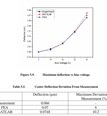
TABLE 5.5. CENTER DEFLECTION DEVIATION FROM MEASUREMENT ... 61
TABLE 5.6. PULL-IN VOLTAGE COMPARISON TABLE... 62
TABLE 6.1. RESONANT FREQUENCY COMPARISON AT 20VDC ... 65
TABLE 6.2. DCBIAS VS RESONANT FREQUENCY COMPARISON TABLE ... 66
TABLE 6.3. TRANS.ANALYSIS DEV. FROM MEAS. WITH VDC=20V AND VAC=20VP-P .. 68
TABLE 6.4. STEADY STATE ANALYSIS DEVIATION FROM MEASUREMENT ... 69
TABLE 6.5. FRACTIONAL BANDWIDTH DEVIATION FROM MEASUREMENT ... 70
TABLE 7.1. EXPERIMENTAL AND THEORETICAL NOISE COMPARISON ... 72
TABLE 7.2. AMPLIFIER OUTPUT DEVIATION FROM THEORY ... 75
LIST OF FIGURES
FIGURE 1.1. CMUT CROSS SECTION [38]. ... 3
FIGURE 1.2. CMUT MODES OF OPERATION. ... 4
FIGURE 2.1. A SECTION OF A MULTILAYER LAMINATED PLATE [38]. ... 14
FIGURE 2.2. CROSS-SECTIONAL VIEW OF A VLSI ON-CHIP INTERCONNECT [38]. ... 17
FIGURE 2.3. EQUIVALENT CIRCUIT MODEL OF CMUT. ... 20
FIGURE 2.4. SIMULINK MODEL OF CMUT. ... 24
FIGURE 2.5. SIMULINK MODEL OF CMUT. ... 25
FIGURE 2.6. MATERIAL DAMPING PROPERTIES ENTRY WINDOW. ... 27
FIGURE 2.7. DYNAMIC ANALYSIS WITH FEA. ... 27
FIGURE 3.1. TRANSIMPEDANCE AMPLIFIER SCHEME. ... 30
FIGURE 3.2. DESIGN GRAPH OF THE TRANSIMPEDANCE AMPLIFIER. ... 33
FIGURE 3.3. PHASE GRAPH OF THE CIRCUIT... 33
FIGURE 3.4. TRANSIMPEDANCE AMPLIFIER. ... 34
FIGURE 3.5. NOISE CALCULATION GRAPH OF TRANSIMPEDANCE AMPLIFIER. ... 36
FIGURE 3.6. FABRICATED PCB. ... 37
FIGURE 3.7. PCB DESIGN FILE. ... 38
FIGURE 4.1. CROSS SECTION OF A SOI WAFER. ... 39
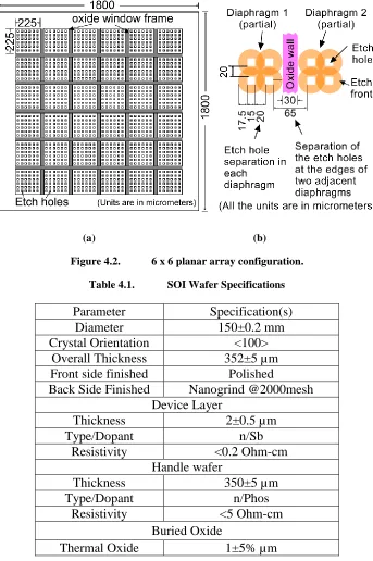
FIGURE 4.2. 6 X 6 PLANAR ARRAY CONFIGURATION. ... 41
FIGURE 4.3. RCA CLEAN. ... 42
FIGURE 4.4. METAL DEPOSITION . ... 43
FIGURE 4.5. PHOTOLITOGRAPHY. ... 44
FIGURE 4.7. METAL AND SILICON ETCH. ... 45
FIGURE 4.8. CHROMIUM ETCHING. ... 45
FIGURE 4.9. SILICON DRIE ETCH. ... 46
FIGURE 4.10. SIO2 ETCH. ... 46
FIGURE 4.11. SEM IMAGE OF A FABRICATED CMUT. ... 47
FIGURE 4.12. SEM IMAGE OF AN ETCH HOLE AFTER DRIE OF SILICON. ... 48
FIGURE 4.13. SEM IMAGE OF A CMUT DIAPHRAGM AFTER RELEASE. ... 48
FIGURE 4.14. SEM IMAGE AFTER BOE. ... 49
FIGURE 4.15. SEM IMAGE OF LATERAL ETCH DISTANCE AT CMUT EDGE. ... 49
FIGURE 5.1. WYKO MEASUREMENT OF WARPING ON CMUT DIAPHRAGM. ... 51
FIGURE 5.2. DIELECTRIC AND DIAPHRAGM LAYER THICKNESS MEAS. WITH SEM. ... 52
FIGURE 5.3. SEM AIR GAP MEASUREMENT FROM CENTER OF THE DIAPHRAGM. ... 53
FIGURE 5.4. BIAS VOLTAGE VS CAPACITANCE. ... 55
FIGURE 5.5. CAPACITANCE CHANGE VS BIAS VOLTAGE. ... 56
FIGURE 5.6. CMUT CROSS SECTION. ... 58
FIGURE 5.7. MEASUREMENT SETUP OF POLYTEC LASER DOPPLER VIBROMETER. ... 59
FIGURE 5.8. PICTURE OF THE CMUT PLANAR ARRAY IN EXPERIMENT. ... 60
FIGURE 5.9. MAXIMUM DEFLECTION VS BIAS VOLTAGE. ... 61
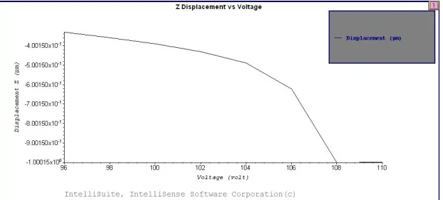
FIGURE 5.10. FEA DISPLACEMENT VS VOLTAGE GRAPH. ... 62
FIGURE 5.11. MIDDLE OF THE DIAPHRAGM WHERE PULL-IN OCCURRED... 63
FIGURE 5.12. PULLED-IN DEVICE CROSS SECTION. ... 63
FIGURE 6.1. DISPLACEMENT VS. FREQUENCY GRAPH. ... 65
FIGURE 6.3. DISPLACEMENT VS. TIME RESULTS WITH VDC=20V AND VAC=20VP-P. ... 67
FIGURE 6.4. DISPLACEMENT VS. FREQUENCY WITH VDC=20V AND VAC=20VP-P . ... 69
FIGURE 6.5. DISPLACEMENT VS BIAS VOLTAGE. ... 71
FIGURE 6.6. 3D SCAN OF CMUT WITH VDC=30V AND VAC=20VP-P AT 113 KHZ. ... 71
FIGURE 7.1. OUTPUT PRESSURE OF BAT-3 TRANSDUCER. ... 73
FIGURE 7.2. TESTBENCH FOR CMUT RECEIVE MODE. ... 73
FIGURE 7.3. SIMULATED CURRENT OUTPUT OF THE CMUT. ... 74
FIGURE 7.4. SIMULATION OF TRANSIMPEDANCE AMPLIFIER. ... 75
FIGURE 7.5. INCOMING RECEIVED SIGNAL. ... 75
FIGURE 7.6. INCOMING RECEIVED SIGNAL, ZOOMED VERSION. ... 76
FIGURE 7.7. PITCH-CATCH MODE TESTBENCH. ... 76
FIGURE 7.8. PITCH-CATCH MODE INCOMING RECEIVED SIGNAL. ... 77
FIGURE 8.1. CROSS SECTION OF A MULTILAYERED SOI WAFER. ... 80
Chapter 1
INTRODUCTION 1.1 Goals
The objective of this project is to design, fabricate and characterize a CMUT (Capacitive Micromachined Ultrasound) array for air-coupled applications such as blind spot monitoring for cars. The CMUTs have become a strong alternative to piezoelectric transducers in medical imaging and immersion applications, however research has been mainly focused on immersion applications, and few research efforts are made for air-coupled CMUTs and their characterization. CMUT‟s enabled wide bandwidth imaging of tissues and vessels and with better resolution [1]. Intravascular ultrasound imaging i another techniques enabled by the CMUT technology which occupies very small area while providing excellent transducer characteristics. Moreover extensive research has been done for non-destructive valuation [2], microphones [3] and smart microfluidic channels [4]. As explained above, much of the research has been focused on immersion applications. This thesis investigates air-coupled CMUT applications such as park assist and blind spot monitoring.
characteristics of the CMUT membrane. For static characterization, experimental data is obtained from optical profilometer, scanning electron microscope and capacitance meter.
For static characterization purposes, the deflection profile of the CMUT membrane is characterized using analytical load deflection model, FEA (Finite Element Analysis) and optical profilometer. Laser vibrometer is used for dynamic characterization in order to obtain steady state response and transient response of the diaphragm. For air-coupled transmission tests, designed readout circuit based on transimpedance amplifier is used to operate the CMUT in receive mode.
This work is believed to provide useful guidance on characterization of CMUTs, therefore bridging the gap between the theory and practice.
1.2 CMUT Operating Principle
Figure 1.1. CMUT cross section [38].
Figure 1.2. CMUT modes of operation.
A control signal operates a switch to enable mode switching from transmit to receive and vice versa as seen in Figure 1.2. Typically, the diaphragm is created using a microfabricated thin film conductor such as aluminum or polysilicon or a composite of a non conducting thin film structural material such as silicon nitride with a thin coating of a conducting material such as aluminum or gold on the top is used. Additionally, to avoid electrical breakdown after collapse due to the pull-in phenomenon, a thin insulation layer, either under the diaphragm conducting material or on the top of the backplate is used. Finally, a passivation layer on the top of the diaphragm is used to protect the CMUT from environmental elements.
As the CMUT‟s sensing characteristics depend on the change of capacitance
1.3 Background
Acoustical sensors have been used for a long time since World War I for underwater imaging and further improvements in piezoelectric materials have been done during World War II [1]. Increased computing power have enabled more complicated algorithms to be run with larger amounts of data from transducers, however the quality of transducers and read out circuit (SNR, bandwidth, etc.) determines the final results of ultrasound systems, therefore making front-end electronics and transducers as the most critical components of ultrasound imaging systems [1] . Recent advances in microfabrication technology made small air gaps to be made, therefore creating very large electric field strengths required for capacitive electrostatic transducers to work effectively, and compete with piezoelectric transducers. CMUTs also offer advantages of larger bandwidth, large arrays with individual electrical connections and integration with microelectronics [7]. As the CMUT‟s improved over the time, the characterization techniques and understanding of the working principles have advanced as well.
Characterization provides the validity of the theory, design methodology and fabrication of the device. It is also useful for making improvements in theoretical equations by data fitting. For static response of CMUT, it is common to use non-contact optical profilometers, which scan the surface of the CMUT under a microscope using optical interferometry method. Another reported static characterization method is called Dynamic Holographic Microscopy [8] , using the principle of holography.
roughness, and a good reflection back to the laser sensor is required [9]. Moreover, their very high cost decreases accessibility of the device.
There are many approaches to design of a readout circuit for CMUTs, including charge amplifier [10], transimpedance amplifier [11] and standard voltage amplifier. Charge amplifier has an advantage of high sensitivity by using charge transfer method, but when the transducer has relatively high DC current leakage, this solution becomes troublesome. Transimpedance amplifier has large bandwidth, good sensitivity and flexibility for many capacitive sensors. Last alternative, voltage amplifiers are not used commonly due to small input impedance of the amplifier and high output impedance of the capacitive sensors.
1.4 Scientific Approach
According to [1], [12] and [13], it has been shown that the static deflection due to electrostatic force and acoustic force can be modelled accurately compared to FEA results. This thesis provides methods and experimental data for validation of the previously developed mathematical models by MEMS Lab. Thesis also extends the static characterization into the dynamic characterization area, in order to accurately predict diaphragm‟s transient response. Non-contact surface profilometer is used in this thesis,
Laser Doppler vibrometer (LDV) is the most accurate method available to characterization researchers for dynamic analysis [15]. LDV extracts the time varying displacement and velocity of the surface due to electrostatic change as a function of time. Steady state response of the diaphragm due to frequency of excitation voltage and transient response due to impulse excitation voltage are obtained with LDV technique.
1.5 Literature Search
In recent years, significant progress has been done in modelling and characterization of the CMUTs in air and immersion applications. The first air coupled CMUT was presented by Stanford researchers M.I. Haller and B.T. Khuri-Yakub [16]. Group fabricated two devices based on work of Mason [17], the transducers were fabricated using standard micromachining techniques. They have used an optical interferometer was used to measure the peak displacement of the 1.8 MHz electrostatic transducer at 230 Å/V.
In [18], 275 x 5600 µm one dimensional CMUT array was characterized successfully, showing good agreement with theory. Device operated at 3 MHz in immersion, with a DC bias of 35V, outputting 5 kPa/V.
metal plate thickness. Authors of [20] state that the equivalent circuit model of the CMUT lacks important features such as coupling to the substrate and the ability to predict cross-talk between elements of an array of transducers. They have proposed the evidence of crosstalk between CMUTs and took precautions including change of its thickness and etched trenches or polymer walls between array elements.
Stanford researchers I. Wygant, M. Kupnik et al. has fabricated CMUTs with vacuum- sealed cavities for transmitting directional sound with parametric arrays for air coupled applications which have resonance frequencies of 46 kHz and 54 kHz, respectively. [21]. Characterization of the CMUTs showed center frequencies of 46 kHz and 55 kHz and 3 dB bandwidths of 1.9 kHz and 5.3 kHz for the 40 µm and 60 µm thick membrane devices, respectively. Although they have achieved a range of 3 m, the devices operate with excessive DC bias and AC excitation voltages that cannot be found outside the laboratories.
M. Torndahl et. al has compared two similar piezoelectric and CMUT transducers using light diffraction tomography method [22]. They have found out superior bandwidth characteristics of CMUTs comparing to piezoelectric transducers.
J. Kiihamaki et al proposed a new concept for SOI MEMS devices, called plug up [24]. They reported a novel process sequence for fabricating micromechanical devices on silicon-on-insulator (SOI) wafers. Authors concluded the advantages of the techniques as improved immunity to stiction and elimination of conductor metal endurance problems during sacrificial etching in hydrofluoric acid. Authors validated their theory with a fabricated CMUT device successfully.
Authors of [25] proposed an SOI based CMUTs and characterized it with an impedance analyzer. Their CMUTs consist of 2700 circular active cells of 65 mm diameter, with 2 mm thick silicon membranes suspended over a 0.5 mm air gap.
S.T. Hansen et al [26] reported air coupled CMUTs with dynamic range larger than 100dB, for non-destructive testing purposes. Experiment was done using two identical transducers facing each other, with a 3 mm thick aluminum plate in the middle of two transducers. The same transducer was used in [27] for ranging, proximity measurement and robotic sensing.
Nicolas Sénégond, Dominique Certon et al. characterized a CMUT with a rarely used method called Digital Holography Microscopy [8]. They provided characterization results for static deflection and roughness tests. Author state that this method provides one of the best tools for statistical evaluation of CMUT.
1.6 Thesis Organization
Chapter 1 starts with the introduction, and summarizes the available literature on CMUT characterization and state-of-art in characterization process. This chapter builds the necessary background for the rest of the thesis.
Chapter 2 presents the method to design CMUTs analytically with Matlab™ and using Intellisuite™ FEA tool.
Chapter 3 presents the method of designing a capacitive readout circuit using based on transimpedance amplifier topology including noise calculations. Important topics like noise figure and printed circuit board are included in this chapter.
Chapter 4 includes the fabrication details and processes that is chosen to fabricate the CMUT. Specifications of the SOI wafer used are given in this chapter. Validation of the fabrication follows the explanation of the fabrication steps.
Chapter 5 of this thesis shows the results of static characterization part of the project. Essential parameters like capacitance, residual stress, stiffness constant, center deflection and pull-in voltage are measured and compared with the theoretical results.
Chapter 6 presents the dynamic characterization results. Simulated and measured parameters are resonant frequency, transient response, steady state response, fractional bandwidth, and specific bandwidth response of CMUT.
Chapter 7 deals with the characterization of readout circuitry which is necessary for the receive operation of the CMUT. Design of a transimpedance amplifier is presented in this chapter. Also, simulation of receive mode and pitch catch mode is presented
Chapter 2
CMUT DESIGN
This chapter described the design methodology adopted to design the capacitive micromachined ultrasound transducers (CMUT) and a transimpedance amplifier based readout circuit. Mathematical models used for designing CMUTs are presented in detail for square membranes. Analytical results are then verified with Intellisuite™ FEA.
Readout circuit is an essential part of CMUT system. It translates the capacitive change of the CMUT to the electrical signal.
2.1 Design Methodology
The final application determines the key parameters of a CMUT such as operating frequency and operating voltage. For air coupled blind spot applications, the operating frequency should be kept as low as possible, without getting interfered by the natural ultrasound noise signals [29]. Capacitance change and deflection of the diaphragm at the operating point are also significant factors to determine the device geometry, operating voltage, and sensitivity. In the design process, initially an analog equivalent circuit model using lumped circuit elements is used to determine approximate behaviour of the CMUT considering geometry, materials, fabrication process, etc. The developed geometry is then analyzed using 3-D electromechanical FEA and modified to optimize the device performance in the target design space. The optimized geometry is then fabricated and characterized to verify the design parameters.
2.2 Center Deflection of CMUT Diaphragm
considered to be homogenous and isotropic with perfect edge conditions. It is also assumed that the clamped edges hold the diaphragm rigidly against any out-of-plane rotation or displacement at the edges but allow displacement parallel to the diaphragm plane. At the edges, out-of-plane displacement is zero and the tangent plane to the displacement surface along the edge coincides with the initial position of the middle plane of the diaphragm. The boundary conditions imposed by the clamped edges can be expressed mathematically as [30-34]:
0 , 0 , 0 , 0 , x a y dy dw y a x dx dw x a y w y a x w (2.1)
During the receive mode operation, the diaphragm experiences two pressure loads: an electrostatic pressure between the backplate and the diaphragm due to the bias voltage and the external mechanical pressure due to the incident acoustical waves. Following the variational method, the combined load deflection model of a clamped single material square diaphragm subject to large deflection due to both electrical and mechanical pressures can be expressed as [35]:
where w0 is the diaphragm center deflection,0 is the residual stress, 0 is the
permittivity of free space, V is the bias voltage, D is the flexural rigidity, PExt is the
external mechanical pressure, and v is the Poisson ratio of the diaphragm material. In (2.2), the term within the first square bracket represents diaphragm stiffness due to nonlinear spring hardening, the first term within the second square bracket represents the stiffness due to the residual stress; the second term within the second square bracket represents the stiffness due to bending, and the third term within the second square bracket represents the spring softening due to the nonlinearity of the electrostatic force. Moreover, in (2.2) the electrostatic pressure due to the fringing field capacitance is neglected as its contribution is negligible compared to the total pressure load. The
constants Cr,Cb, and Cs are determined by adjusting the analytical solution with the numerical results for a specific design space and following [36] their values for typical thin diaphragms are:
. . , . C , . C b r 994 1 C and 06 4 45 3 s (2.3)
The Poisson ratio dependent function fs
in (2.2) is given by [36]:
1 271 . 0 1 s f (2.4)Equation (2.2) can be modified to determine the load-deflection characteristics of a multilayered diaphragm as shown in Figure 2.1 by replacing the flexural rigidity D
Figure 2.1. A section of a multilayer laminated plate [38].
Following Figure 2.1, the effective flexural rigidity Deff is expressed as:
A B AC Deff 2 (2.5)
where the constants A, B and C are expressed as:
),
( 1
kk k k t t Q A (2.6) ), 2 ( 1 2 2
k k k k t t Q B (2.7) ), 3 ( 1 3 3
k k k k t t Q C (2.8) and k k k v E Q 2 1 (2.9)where Ek and vk are the Young‟s modulus and the Poisson‟s ratio of the kth layer
respectively. In (2.2), the effective Young‟s modulus E~ is the plate modulus and is
2 1 ~ E E (2.10)
whereE is the Young‟s modulus of the diaphragm material. As the thickness of the top conducting layer is much lower compared to the thickness of the structural diaphragm material, considering only the Young‟s modulus, Poisson ratio, and the residual stress of
the main structural layer to determine the nonlinear stiffness associated with the spring hardening and the stiffness due to the residual stress in (2.2) would not introduce any significant error.
The effective airgap deff is defined as:
o ri i rm m eff d d d
d
(2.11)
where, dm is the membrane thickness, di is top electrode thickness, rm is dielectric
constant of the membrane, ri is dielectric constant of the top electrode and do is air gap distance between diaphragm and backplate.
The real root of the 3rd order polynomial (2.2) represents the center deflection of the diaphragm subject to both electrostatic and external pressure. Two other roots are imaginary and have no practical significance.
As the diaphragm lies in the x-y plane, the parallel plate capacitance between the deformed diaphragm and the backplate can be calculated following [37]:
A deff w x y
dxdy C
, 0
In (2.12) w
x,y represents the deflection surface of the deformed diaphragm alsoknown as the deflection shape function.
2.2.1 Deflection Shape Function
Following [38], the deflection profile of a multilayered diaphragm as used in typical CMUTs can be determined from:
N n n n a y x c a y a x w w 2 , 1 , 0 2 2 2 2 2 2 2 2 20 1 1 (2.13)
where w0 is the diaphragm center deflection determined using (2.2) and the coefficients
n
c are adjustable parameters to be determined from FEA simulation results for any
particular design space. For typical CMUT design space (diaphragm thickness range of 0.5-3 m and sidelength range of 200-1000 m), investigation shows that three terms (N 2) in (2.13) are necessary for large deflection cases while only two terms (N 1) are necessary for small deflection cases to achieve a high degree of accuracy. For the
specified design space, the parametersc0,c1, and c2are determined as:
h c h c c 0005 . 0 0011 . 0 1 2 1 0 (2.14)
by comparing the results from (2.13) with 3-D FEA using IntelliSuite.
2.3 Capacitance
diaphragm sides and charge concentration at the diaphragm edges. Though an accurate value of the fringing field capacitance can only be obtained by solving Poisson‟s equation using a 3-D field solver, a highly accurate value of the fringing field capacitance can be calculated by modifying a VLSI on-chip interconnect capacitance model presented in [35].
Figure 2.2. Cross- sectional view of a VLSI on-chip interconnect separated from a fixed ground plane by a dielectric medium [38].
Following [35], the per unit length capacitance of a VLSI on-chip interconnect of width wOCI and thickness hOCI, separated from the substrate by a dielectric medium of
thickness d0OCI and relative dielectric constant r, as shown in Figure 2.2 can be
expressed as: 5 . 0 0 25 . 0 0 0
0 0.77 1.06 1.06
OCI OCI OCI OCI OCI OCI r OCI d h d w d w
C (2.15)
4 / h 0.1 , 1
/ 0OCI OCI 0OCI
OCI d d
w and 6% as long as
10 , 3 . 0
/ 0OCI OCI 0OCI
OCI d h /d
w holds. An approximate value of the fringing field
capacitance for a CMUT fabricated with a square diaphragm of sidelength 2aas shown in Figure 1.1 can be calculated by modifying (2.15) as:
5 . 0 25 . 0 2 12 . 2 2 12 . 2 44 . 1 4 eff c eff eff d d a d a a a d a
C (2.16)
The first term in (2.16) represents the parallel plate capacitance associated with the CMUT as shown in Figure 1.1. The second and third term together represent the fringing field capacitance due to the diaphragm sidelength 2a while the fourth term
represents the fringing field capacitance due to the conductor thicknessdc. By
rearranging (2.16), a functional form of total capacitance associated with a CMUT can be derived as: ) 1 ( ff 0 C C
C (2.17)
whereC0 is the parallel plate capacitance expressed as
eff d a C 2 0 0 4 (2.18)
and Cff is the fringing field factor expressed as:
0.5 75 . 0 ff 53 . 0 2 1 06 . 1 385 . 0 eff c effeff d d
a d
a d
a
C
The third term in (2.19) represents the fringing field capacitance due to the conductor thickness dc and can be neglected as the flux lines originating from the
conductor sides along the thickness will terminate beyond the coupling area of the device and will not contribute to the total capacitance.
After deformation, the total capacitance is also contributed by two factors: the parallel plate capacitance CDeform between the deformed diaphragm and the backplate
which can be calculated using (2.12), and the fringing field factorCff. Thus the total
capacitance after deformation can be expressed as:
) 1
( ff
Deform C C
C (2.20)
As the diaphragm edges are rigidly fixed and don‟t undergo any deformation and
as the fringing field capacitance is contributed mainly by the charges concentrated at the
edges, the fringing field factor Cff can be assumed to remain unchanged despite
diaphragm deformation and (2.19) can be used to calculate Cff as before.
2.4 CMUT Lumped Element Model
Lumped element modeling is used to reduce the complexity of CMUT modeling to a manageable level for rapid and efficient simulation. This includes modeling of all major sensor performance criteria such as, resonant frequency, damping effects, radiation resistance, sensitivity due to bias voltage, etc.
represents air mass. Mm is diaphragm mechanical mass and its compliance is Cm. the air gap and movable plate vent losses are represented by resistances Rg and Rh, and the air gap compliance is Ca.
Figure 2.3. Equivalent circuit model of CMUT.
The acoustic impedance of the air in contact with the vibrating diaphragm is represented by radiative resistance Rr and air mass Mr.
c a Rr
2 4 4 0
(2.21)
3 8 0a3
Mr (2.22)
where ρ0 is the air density, c is the sound velocity, and ω is the angular vibration frequency. The diaphragm compliance is equal to the average diaphragm deflection divided by the applied force. It is estimated from the energy method:
D a T
a C
eff
m 6 2 2
2
2 32
(2.23)
d
t
T (2.24)
where is the residual stress of the diaphragm.
The equivalent mass element Mm is derived from kinetic energy of the square diaphragm under the uniform loading.
T
T a D
Mm eff
64
2 2 2
4
(2.25)
where ρ is mass per unit area of the diaphragm.
The viscosity loss in the air gap Rg and its compliance Ca are:
8 3 4 ln 8 2 12 2 3 2 sf sf sf g nd uaR
(2.26)
2 2 2 0c a
d C
sf
a (2.27)
where n is the hole density in the diaphragm and sf is the surface fraction occupied by
the holes, u is the air viscosity coefficient, and d is the average air gap distance. Also viscosity loss of the diaphragm plate holes can be approximated as:
4 2 8
nr uha
Rh (2.28)
Equivalent impedance Zt of the CMUT is expressed as:
a h g h g m r r t C R R ω j R R C ω j M M ω j R Z ) ( 1 1 The total sensitivity St of the CMUT is defined as the output voltage Vo per unit
of incident acoustical pressure P and can be expressed as [39]:
t b t dZ ω j a V P V S 2 0
(2.30)
where Vb is the bias voltage. Also, resonant frequency is estimated with [39]:
4 2
2 2 1 a T a D
fres eff
(2.31)
2.5 Stiffness and Residual Stress
Stiffness and residual stress are key parameters for both static and dynamic analysis of the CMUT displacement. Stiffness is calculated from the relationship between the mass and resonant frequency. After measuring the resonant frequency, then the stiffness parameter is extracted then from the known relationship between mass and resonant frequency which is;
m k
w0 (2.32)
From the extracted stiffness, residual stress of the diaphragm is calculated using the equation from [40]:
4 2 12 a D C a t C
2.6 Pull-in Voltage
If the bias voltage exceeds certain limits, the electrostatic attraction force between the diaphragm and the backplate overcomes the elastic restoring force associated with the diaphragm and the diaphragm collapses on the backplate resulting in a device failure [37]. This voltage is known as the pull-in voltage. Determining the pull-in voltage is critical in the design process in order to determine the optimum DC operating point of the CMUT as increasing the DC bias voltage increases the sensitivity of the device. The pull-in voltage for a square diaphragm CMUT as shown pull-in Figure 1.1 can be calculated following: 25 . 1 75 . 0 2 0 3 4 4 2 2231 . 0 665 . 0 3 9 ~ ) ( 12 eff eff eff s s eff b r pi d a d d a h E v f C a D C a h C V (2.34)
2.7 Simulink Model for Dynamic Analysis
For Dynamic simulation, first order parallel plate capacitor model [41] and FEA methods are used. First order model is computationally efficient and reaches very good accuracy which is a derivation of the parallel plate actuator model represented in [37]. The model is built on Matlab/Simulink using building blocks as in Figure 2.4 and Figure. Fundamental equation of motion for an electrostatic parallel plate actuator can be modeled as:
2
0 ( )
g t V AV kx x b x
where A is area, 0 is permittivity of air, g is the air gap distance, m is mass, b is
damping factor and k is the stiffness parameter.
Since (2.35) expresses position as a function of time, continuous iteration is necessary to solve the equation to determine the diaphragm position as a function of time. In (2.35) the stiffness parameter k is determined from material properties and geometric specifications of the diaphragm and the mass m can be calculated from the known volume and density of the diaphragm material. The damping factor b can be calculated following [37]:
Q mw
b 0
(2.36)
where Q is the quality factor. As the mass m and the angular resonant frequency w0 is
known, then damping factor b can easily be calculated. A Simulink model as shown in Figure 2.4 then can be built to solve (2.35) to determine the dynamic response of the system.
Figure 2.5. Simulink model of CMUT.
2.8 FEA Model for Dynamic Analysis
Intellisuite™ FEA package is used for dynamic analysis of the CMUT. In order to
run a successful dynamic analysis, Rayleigh damping coefficients (mass damping factor) and (stiffness damping factor) are determined from [42]:
2 2
i
i i
(2.37)
The associated quality factor is expressed as:
i i
Q
2 1
(2.38)
Once a set of Qi are determined (Table 2.4) from a frequency analysis with
resonant modes (Table 2.2), respective damping factors i can be determined from
(2.38). The values of ialong with i are then inserted in (2.37) and solved
simultaneously to obtain and . Then, these values are inserted into the damping
method with squeezed film damping has been chosen to carry out the transient analysis using FEA with IntelliSuite™.
2.9 Final Design Specifications
Following the mathematical models and design methodology presented above, a CMUT has been designed and analytically analyzed. Final design specifications of the CMUT are summarized in Table 2.1.
Table 2.1. Final CMUT Design Specifications
Parameter Value Unit
Operating Frequency Range 113-167 kHz
Operating Voltage 20 VDC
Resonant Frequency 614 kHz
Pull-in voltage 110 VDC
Airgap 1 µm
Diaphragm thickness 2 µm
Diaphragm Sidelength 225 µm
Number of CMUTs in an Array 6x6 -
Array Sidelength 1.8 mm
Vent Hole Dimension 15x15 µm
Number of Vent Holes 5x5 -
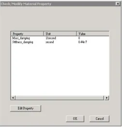
For FEA simulation of the transient response, a large displacement option with 10 iterations and an increment number of 70 has been used as shown in Figure 2.7. For steady state analysis, first six mode Rayleigh damping coefficients are calculated and fed into the simulation to reach the best accuracy. Respective i values are presented in
Figure 2.6. Material damping properties entry window.
Table 2.2, Table 2.3, Table 2.4 represents mode frequency, mode damping ratio and mode quality factor values respectively.
Table 2.2. Frequency with Respect to Mode Number
Mode Number Frequency (MHz)
1 0.614
2 1.3
3 1.35
4 2.048
5 2.49
6 2.5
Table 2.3. Damping Ratio with Respect to Mode Number
Mode Number Damping Ratio (i)
1 0.086
2 0.1865
3 0.1865
4 0.282
5 0.344
6 0.345
Table 2.4. Quality Factor With Respect To Mode Number
Mode Number Quality Factor (Qi)
1 5.81
2 2.68
3 2.68
4 1.77
5 1.45
Chapter 3
READOUT CIRCUIT
This chapter presents the design and implementation of a readout circuit developed for use with the CMUT to generate a voltage signal in response to an ultrasound excitation which is an essential part of the CMUT system. Readout circuit translates the capacitive change of the CMUT due to an ultrasound excitation to a useful electrical signal. The basic theory of transimpedance amplifier is, when a CMUT‟s capacitance changes due to external ultrasound pressure, this change is capacitance will require charges to flow from DC bias supply. Due to transimpedance amplifier‟s feedback mechanism, this flowing current is forced to pass through a feedback resistor
RF, connected between the input and output ports of an operational amplifier (Figure 3.1), causing an output voltage from the transimpedance amplifier.
3.1 Design of a Transimpedance Amplifier
where
f f
f R
sC
Z 1 || (3.2)
and Vo, Iin, ZCMUT and A(s) are the output voltage, input current, complex impedance of the CMUT and the open loop gain of the operational amplifier respectively.
Figure 3.1. Transimpedance amplifier scheme.
Since transimpedance amplifier is a feedback amplifier structure, feedback factor
F should be calculated, which is basically how much of the output is fed back to the input of the amplifier:
From knowledge of the feedback factor, the noise gain of the amplifier can be calculated following:
in Z
f Z
F
1 1 Gain
Noise (3.4)
It is necessary to design the transimpedance amplifier in such a way that the I-V gain doesn‟t have a peak caused by a zero introduced due to the capacitance of the
CMUT. In order to overcome this zero, a feedback capacitor CF is introduced in parallel to RF simply because of stability issues. If the capacitance of the CMUT is large enough, and the amplifier is not compensated with a feedback capacitor, the overall system becomes prone to serious ringing and oscillation problems. The gain vs. frequency and phase vs. frequency plots of typical transimpedance amplifiers are shown in Figure 3.2 and Figure 3.3 respectively. The Matlab codes for the figures are presented in Appendix A. From the figures, it can be concluded that to design a stable transimpedance amplifier, noise gain curve should be flattened before it crosses the open loop gain line of the operational amplifier.
The CMUT capacitance introduces a zero to the system which is:
CMUT F Z
C R f
2 1
(3.5)
F F p
C R f
2 1
(3.6)
However, besides cancelling the zero, this pole also introduces a phase margin of 45º at fP , stabilizing the circuit and prevent peaking in the I-V Gain graph. It is to be noted that 45º is a theoretical estimation and the actual phase margin (PM) does vary for different implementation. A comparison between Matlab simulated design parameters and Spice parameters are presented in Table 3.1.
Table 3.1. Matlab and Spice Comparison Table
Opamp BW
(MHz) Rf (kΩ) Cf (pF) Cs (pF) f-3db (kHz) Phase Margin (°)
Spice 14 MHz 75 4.7 65 675 55
Matlab 14 MHz 75 4.7 65 63
6% Deviation
58 5.1% Deviation
Where
GBW is the Gain Bandwidth product of the operational amplifier
Rf is the feedback resistor on the feedback loop of the operational amplifier.
Cf is the feedback capacitor on the feedback loop of the operational amplifier, which is used for stability of the transimpedance amplifier topology.
Cs is the CMUT capacitance.
f-3db is the cutoff frequency of the transimpedance amplifier.
Figure 3.2. Design graph of the transimpedance amplifier.
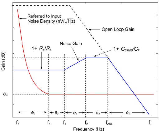
3.2 Noise
Noise of the transimpedance amplifier can be derived from the circuit in Figure 3.4. In Figure 3.5, noise regions of the system are clearly indicated. The first noise region
f1 is a result of the zero introduced by the input sensor capacitance, and is represented as:
RS RF
Cin f|| 2
1
1 (3.7)
whereCin CS CC CAMP, CC is cable capacitance and CAMP is amplifier input
capacitance.
Figure 3.4. Transimpedance amplifier.
Second noise region f2 is a pole introduced by inserting the feedback capacitor, in order to stabilize the transimpedance amplifier, and is expressed as:
RS RF
CF f|| 2
1
2 (3.8)
Operational amplifiers open loop gain frequency, fAOL is estimated as:
in F
u AOL
C R
f f
2
AOL
F represents the intersection of the noise gain and open loop bandwidth where
u
f is the gain bandwidth product which indicates the bandwidth of the operational
amplifier. After defining the noise regions, RMS noise of the first region e1is calculated as: a b S F f f B R R
e1 1 ln (3.10)
where B is operational amplifiers input noise density at 1 Hz and fa=1 Hz
Second and other noise regions are calculated as multiplying the area under the closed loop gain and amplifier noise density curves. Second region‟s RMS noise e2 is calculated following:
b n
S
F e f f
R R
e
1
2 1 (3.11)
where fb is 1/f noise corner frequency. Third, fourth and fifth noise region noise values are calculated as:
3 3 1 1 3 1 3 2 1 3 f f f e R R e n S F (3.12) 2
4 1 e f f
C C
e n AOL
F
in
(3.13)
u AOL
n F in f f e C C
e
2 1 5 (3.14)
The feedback resistor RF contributes to total noise of the amplifier, which is calculated as: BW
KTR
eR 4 F (3.15)
2 2 5 2 4 2 3 2 2 2 1 ) _
(NOISE RMS R
OUT e e e e e e
V (3.16)
RMS noise calculation is carried out using the values represented in Table 3.2.
Figure 3.5. Noise calculation graph of transimpedance amplifier.
Table 3.2. Transimpedance Circuit Component Values
Component Value Unit
Operational amplifier bandwidth (LT1122) 14 MHz Feedback resistor RF 75 kΩ Feedback capacitor CF 4.7 pF Cable capacitance Cc 2 pF Operational amplifier input capacitance CAMP 4 pF
3.3 Printed Circuit Board
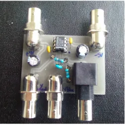
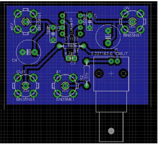
generated in EAGLE PCB Design software, then translated into universal Gerber files and fed into the PCB Prototyping machine. Fabricated PCB is presented in Figure 3.6.
Figure 3.6. Fabricated PCB.
Chapter 4
FABRICATION
This chapter presents a step by step description of the process sequence followed to fabricate the CMUTs on silicon on insulator (SOI) wafers using a single mask. Scanning electron microscopy (SEM) has later been used for geometrical verification of the fabrication process. The details of each fabrication step is provided with operating conditions, used materials, process type and a conceptual cross sectional view has been provided.
4.1 SOI Wafers
CMUTs are typically fabricated using the surface micromachining technique or using a SOI wafer. In the surface micromachining technique, a CMUT is fabricated with a silicon nitride or polysilicon structural diaphragm coated with a thin layer of conducting material such as gold or aluminum on the top. The air cavity is realized by sacrificial etching of a low temperature deposited silicon dioxide layer on the top of a passivated silicon wafer. On the other hand, the SOI wafers come with a buried oxide layer (BOX) sandwiched between a single crystal device layer and a handle layer as shown in Figure 4.1.
Small holes are created in the device layer to facilitate entry of the silicon oxide etchant such as buffered oxide etch (BOE) to dissolve the oxide layer to create the cavity. The overall process is simpler than the surface micromachining technique. Additionally, the SOI wafers offer superior electrical and mechanical qualities such as: 1) higher switching speeds [44], 2) higher quality factor, 3) lower residual stress, and 4) better thickness uniformity when compared to other diaphragm material like Si3N4 and Polysilicon. Based on these considerations, an SOI based fabrication process has been selected to fabricate the CMUTs.
4.2 Mask Preparation
Only a single mask is necessary to fabricate the CMUTs on an SOI wafer. CMUTs are designed to be fabricated as a 6 x 6 planar array separated by a thin strip of silicon dioxide as shown in Figure 4.2a. Each of the CMUTs in the planar array has a sidelength of 225 µm, a diaphragm thickness of 2 m, and an airgap of 1 m as listed in
middle of the diagonal distance between two etch holes to ensure that the buried oxide layer is removed and the diaphragm is released properly at the farthest distance. Material properties and geometrical specifications of the SOI wafer used to fabricate the CMUTs are listed in Table 4.1.
(a) (b)
Figure 4.2. 6 x 6 planar array configuration. Table 4.1. SOI Wafer Specifications
Parameter Specification(s)
Diameter 150±0.2 mm
Crystal Orientation <100> Overall Thickness 352±5 µm Front side finished Polished
Back Side Finished Nanogrind @2000mesh Device Layer
Thickness 2±0.5 µm
Type/Dopant n/Sb
Resistivity <0.2 Ohm-cm Handle wafer
Thickness 350±5 µm
Type/Dopant n/Phos
Resistivity <5 Ohm-cm Buried Oxide
4.3 Fabrication Steps Step 1: RCA Clean
Figure 4.3. RCA clean.
Before the SOI wafers are subject to any microfabrication process, an RCA cleaning is necessary to clean all organic contaminants, oxide layers and heavy metal contamination that may build up on the wafer surface. In the RCA cleaning, the first step is removal of all organic coatings in a strong oxidant, such as a 7:3 mixture of concentrated sulphuric acid and hydrogen peroxide (“pirhana”). Then organic residues are removed in a 5:1:1 mixture of water, hydrogen peroxide, and ammonium hydroxide. As this step can grow a thin oxide on silicon, it is necessary to insert a dilute HF etch to remove this oxide when cleaning a bare silicon wafer. The HF dip is omitted when cleaning wafers that have intentional oxide on them. Finally, ionic contaminants are removed with a 6:1:1 mixture of water, hydrochloric acid, and hydrogen peroxide [37]. The RCA cleaned wafer cross section is shown in Figure 4.3.
Step 2: Metal Deposition (Chromium and Gold)
Figure 4.4. Metal deposition .
Step 3: Photolitography
Figure 4.5. Photolitography.
After deposition of the electrode layer, pattern of etch holes must be developed. These etch holes provides a router for etching the buried oxide layer (SiO2) as well as reducing the air damping during diaphragm deflection. For photolithography process, a 0.5 m thick Shipley 1805 photoresist has been spin deposited using a thin HMDS layer as the primer (Figure 4.5). After soft baking of the photoresist layer, the wafer was exposed to UV light to carry out the photolithography and the final pattern was developed as seen in Figure 4.6.
Step 4: Metal (Gold and Chromium) and Silicon Etch
Figure 4.7. Metal and silicon etch.
Figure 4.8. Chromium etching.
Figure 4.9. Silicon DRIE etch.
Step 5: Dicing and Photoresist Removal
After etching of silicon and devices are ready for release, it is important to get the individual dies separated. Dicing process is carried out before the photoresist removal, in order to protect the CMUT‟s diaphragm from heat, pressure and any failures due to
dicing saw. After the dicing process, photoresist was stripped.
Step 6: Release and Critical CO2 Drying
In order to release the diaphragm, Transene Improved BOE (4-8% HF + NH4F, etch rate~800A/min) has been used to sacrificially etch the oxide layer which is followed by critical point drying in a typical CPD dryer (Figure 4.10). Critical point drying is carried out to avoid stiction of the devices.
4.4 SEM Validation of Fabricated CMUT Geometry
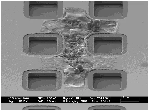
After drying, the dies were inspected in SEM to check for proper diaphragm release. Figure 4.11 shows SEM image of one of the sensor diaphragms. Figure 4.12 shows the SEM image of one of the DRIE etched holes before oxide release and Figure 4.13 shows diaphragm after release.
Figure 4.14 shows the SEM measurement across the diagonal distance between two etch holes. From
Figure 4.14, it is clear that the diagonal distance between two etch hole corners of 29.07 m matches very closely with the mask value of 28.28 m and the oxide layer has
been completely etched in that region. The designed 17.5 m lateral distance of an etch hole from the CMUT edge (Figure 4.2b) also matches very closely with SEM measured value of 18.03 m as shown in Figure 4.15.
Figure 4.12. SEM image of an etch hole after DRIE of silicon.
Figure 4.13. SEM image of a CMUT diaphragm after release.
Figure 4.14. SEM image after BOE showing the release of the SiO2 layer in the diagonal region between two etch holes.
Figure 4.15. SEM image of lateral etch distance at CMUT edge.
These results conclude that the accuracy of the fabrication process is very good.
Chapter 5
STATIC CHARACTERIZATION
This chapter presents the detailed methodology of static characterization of the fabricated CMUTs. The methodology involves experimental measurement of key static device parameters and comparing them with analytical and FEA results to verify the design process. The key measured parameters are: diaphragm and airgap thicknesses, diaphragm static deflection, diaphragm stiffness, pull-in voltage, and static capacitance of the CMUT. Scanning electron microscope, Polytec laser Doppler vibrometer, LCR meter, and optical profilometer are used for measurements. Very good agreement has been found between the measured, calculated, and simulated values.
5.1 SEM and Optical Profilometer Analysis
As the microfabrication process is associated with some level of uncertainty in the thickness of the deposited layer and as the vendor supplied SOI wafers come with a certain percent variation in the thickness of the device layer and the oxide layer as listed in Table 4.1, it is necessary to measure the actual thickness of the diaphragm and the airgap for use in the simulation models to validate the design process. Any deviation in these values will cause discrepancy between simulation and experimental results. In order to achieve the most accurate results, SEM analysis is done at the University of Western Ontario Nanofabrication facility and the optical profilometer analysis is done at the Tribology lab at the University of Windsor.
![Figure 1.1. CMUT cross section [38].](https://thumb-us.123doks.com/thumbv2/123dok_us/1441088.1176528/22.612.199.451.69.278/figure-cmut-cross-section.webp)