Electrical Properties of Low-Temperature Processed
Sn-doped In
2
O
3
thin films: The Role of
Microstructure and Oxygen Content and the Potential
of Defect Modulation Doping
Getnet K. Deyu1,2, Jonas Hunka1, Hervé Roussel2, Joachim Brötz3 , Daniel Bellet2and Andreas Klein1,*
1 Technische Universität Darmstadt, Department of Materials and Earth Sciences, Electronic Structure of
Materials, Otto-Berndt-Straße 3, 64287 Darmstadt, Germany
2 Univ. Grenoble Alpes, CNRS, Grenoble INP, LMGP, 38 000 Grenoble, France
3 Technische Universität Darmstadt, Department of Materials and Earth Sciences, Structural Research,
Otto-Berndt-Straße 3, 64287 Darmstadt, Germany
1
2
3
4
5
6
7
8
9
10
11
12
13
14
15
* Correspondence:[email protected];Tel.:+49-6151-16-20772
Abstract:Low-temperatureprocessedITOthinfilmsofferthepotentialofovercomingthedoping limit bysuppressing the equilibrium of compensatingoxygen interstitial defects. To elucidate thispotential,electricalpropertiesofSn-dopedIn2O3(ITO)thinfilmsarestudiedindependence
on filmt hickness.I n-operandoc onductivitya ndH alle ffectm easurementsd uringa nnealingof roomtemperaturedepositedfilmsw ithd ifferentfi lmth icknessindi fferenten vironmentsallow todiscriminatebetweentheeffectsofcrystallization,graingrowth,donoractivationandoxygen diffusiononcarrierconcentrationsandmobilities.At200◦C,acontrolofcarrierconcentrationby oxygen incorporationorextractionisonlypossibleforverythinfilms.Theelectricalproperties ofthickerfilmsdepositedatroomtemperaturearemostlyaffectedbygrains ize.Theremaining diffusivity ofcompensatingoxygen defectsat200◦Cissufficientt os creent heh ighF ermilevel inducedbydepositionof Al2O3 usingatomiclayerdeposition(ALD),whichdisablestheuseof
defectmodulationdopingatthistemperature. Theresultsindicatethat achievinghighercarrier concentrationsrequiresacontroloftheoxygenpressureduringdepositionincombinationwithseed layerstoenhancecrystallinityortheuseofnearroomtemperatureALD.
Keywords: ITO;electrical properties;dopinglimits; modulationdoping; thicknessdependence; low-temperaturedeposition
16
1. Introduction 17
Transparent conductive oxides (TCOs) are key materials for electrodes in display and solar cell
18
technologies [1–6]. The most prominent examples are Sn-doped In2O3(ITO), Al-doped ZnO (AZO)
19
and F-doped SnO2(FTO), which are degenerately doped n-type semiconductors. Highest electrical
20
conductivities of∼104S/cm are obtained with ITO having carrier concentrations of 1−2×1021cm−3
21
and mobilities of∼40 cm2/Vs [7]. Even higher conductivities are desirable, for example to reduce
22
optical losses in solar cells by using thinner TCOs or wider cells in thin film modules. The conductivity
23
can be increased either by a higher carrier concentration or a higher carrier mobility.
24
If thermodynamic equilibrium of defect concentrations can be established, the concentration of
25
free electrons in TCOs is limited by formation of self-compensating intrinsic defects [6,8–10]. In the case
26
of donor-doped In2O3, the compensating defect species is interstitial oxygen [10–15]. Consequently,
27
the diffusion of oxygen is required to establish defect equilibrium. At the limit of electrical conductivity,
28
the addition of more donors does then not result in an increase of the concentration of free electrons
29
but in that of interstitial oxygen. The carrier concentration can also be limited if the dopants are not
30
completely dissolved in the material but form separate phases or segregate to grain boundaries and
31
surfaces. Segregation requires mobile dopants. Both oxygen and dopant (Sn) diffusion in ITO have
32
been demonstrated to occur already at 300◦C [16–19].
33
If samples are processed at temperatures low enough to suppress oxygen diffusion and dopant
34
segregation, defect equilibrium cannot be established. In such a case, the concentration of compensating
35
defects could be lower than in equilibrium. Low processing temperatures of TCOs do therefore offer
36
the potential advantage of achieving higher carrier concentrations. In contrast, in the case of In2O3,
37
conductivities of films deposited at lower temperature (.200◦C) are in most cases lower than those of
38
films prepared or annealed at higher temperature. In particular, films prepared at room temperature
39
have conductivities below 103S/cm, mostly because of lower carrier concentrations [20–24]. Films
40
prepared at room temperature are often amorphous. In this case, the carrier concentration does
41
not depend on donor concentration but is rather determined by the oxygen stoichiometry [25,26].
42
Enhanced crystallization of room temperature deposited films has been achieved using Fe2O3seed
43
layers [27]. Thereby, the carrier concentration can be enhanced by about one order of magnitude due
44
to donor activation but remain below 1021cm−3.
45
Recently, Koida and coworkers have demonstrated that high conductivities of differently doped
46
In2O3films can be obtained by annealing room temperature deposited films to∼200◦C [28–30]. There,
47
the addition of H2O during deposition can induce substantial grain growth during annealing and
48
result in very high carrier mobilities of up to∼140 cm2/Vs. However, while the low temperature
49
processing provides an advantage regarding temperature sensitive substrates and the high mobility
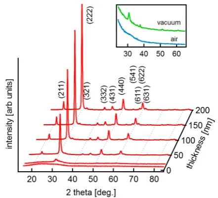
50
leads to an enhanced optical transparency in the infrared, the films still exhibit carrier concentrations
51
lower than 1021cm−3. There is yet no evidence that carrier concentration above 2×1021cm−3can be
52
achieved by lower substrate temperatures.
53
As the conductivity of ITO is determined by a number of factors including crystallinity, grain
54
size and oxygen content, which differently impact carrier concentration and mobility, it is difficult
55
to discriminate between the different influences. This becomes particularly important for the
56
identification of the conditions needed to achieve higher carrier concentrations by low temperature
57
processing.
58
In the present work, we have studied the effect of low temperature (≤200◦C) processing on the
59
electrical properties of ITO thin films with different film thickness. Together with in-operando Hall
60
effect measurements, it becomes possible to discriminate between the effects of crystallization, grain
61
growth, donor activation and oxygen diffusion on carrier concentrations and mobilities. The results
62
provide guidelines for low-temperature processing of doped In2O3films and will be used to explain
63
the effects of Al2O3deposition on the electrical properties of ITO and the conditions for realizing
64
defect modulation doping of this compound. Defect modulation doping utilizes a Fermi level in a
65
contact phase, which is pinned by defects at a high energy [31]. Carrier concentrations higher than
66
those observed by conventional doping can be achieved by this technique near an interface. A suitable
67
material with a high Fermi energy is obtained by low-pressure atomic-layer-deposited Al2O3[32].
68
2. Experimental 69
ITO and Al2O3films were prepared in the Darmstadt Integrated SYstem for MATerials research
70
(DAISY-MAT), which combines several home-made deposition chambers with a multi-technique
71
surface analysis system in a single ultrahigh vacuum cluster tool [6]. ITO films were deposited on
72
quartz glass substrates by magnetron sputtering with radio-frequency (RF) excitation. The background
73
pressure of the deposition chamber was 10−6Pa. A ceramic 2 inch ITO target with 10 wt% SnO2doping,
74
a RF power of 25 W, a process pressure of 0.5 Pa, an Ar flux of 6.6 sccm and a target-to-substrate
75
distance of 10 cm were used for deposition. The film thickness of ITO was varied from 8–200 nm and
76
the substrate temperature during deposition from room temperature to 400◦C.
77
Al2O3 was deposited using a low-pressure process in a separate vacuum chamber with a
78
background pressure of 10−6Pa using Trimethylaluminium (TMA) from SAFC Hitech and purified
water as precursors. The setup and Al2O3deposition are described in detail in [32]. The ALD pulse
80
lengths were set using ALD 3 series valves (Swagelock) with a microelectronic control unit to 80 ms for
81
TMA and 150 ms for water. Pumping continued during exposure and each exposure was followed by
82
pumping for 300 s, resulting in a total duration of an ALD cycle of 10 min. The growth of aluminum
83
oxide was carried out at a substrate temperature of 200◦C.
84
X-ray photoelectron spectroscopy (XPS) measurements were performed without breaking
85
the vacuum using a Physical Electronics PHI 5700 (Physical Electronics Inc., Chanhassen, MN)
86
spectrometer. Monochromatic Al Kαradiation at an emission angle of 45◦and with an excitation energy
87
of 1486.6 eV was used for XPS measurement. The binding energies of the spectrometer are regularly
88
calibrated by a clean sputter cleaned silver sample. Coplanar grazing incidence X-ray diffraction
89
(GIXRD) patterns were collected with a Bruker D8 Advance Series II (Bruker AXS, Karlsruhe, Germany)
90
and a Rigaku SmartLab (Rigaku, Tokyo, Japan) diffractometer in the 2θrange of 15–85◦using Cu Kα
91
radiation with a weighted wavelength of 1.54186 Å. Room temperature and temperature dependent
92
Hall-effect measurements were carried out in van-der-Pauw geometry using a custom-made setup,
93
which allows for continuous measurements with controlled temperature, pressure and gas composition
94
[18,33].
95
3. Results and Discussion 96
3.1. Influence of substrate temperature and film thickness
97
As a first step, the influence of substrate temperature on the electrical properties of ITO thin films
98
with different thickness is presented in this section. Films deposited at elevated substrate temperature
99
are expected to be crystalline but films grown at room temperature might be amorphous [20,25,34,35].
100
To verify this, X-ray diffraction patterns recorded in grazing incidence of the films deposited at room
101
temperature are shown Fig.1.
102
Figure 1.Grazing Incidence XRD patterns of ITO films with different film thickness deposited at room temperature. The indexed lattice planes correspond to those of cubic In2O3(International Centre for Diffraction Data (ICDD) card 00-006-0416-High-bcc). The insert shows grazing incidence diffraction patterns of two 10 nm thick films annealed at 200◦C in air or vacuum, respectively (see section3.2).
The thinnest film doesn’t show any reflections. This is not due to the low film thickness as
103
clear reflections are observed after annealing the same film (see insert; the effect of annealing is
104
described in section3.2). With increasing film thickness the diffraction peaks associated to In2O3are
Figure 2.Conductivity (a), carrier concentration (b) and carrier mobility (c) of ITO films deposited at room temperature, 200◦C and 400◦C as a function of film thickness.
increasing. Hence, only the thinnest film is completely amorphous after deposition. The increasing
106
crystallinity with film thickness has been observed previously and can be attributed, on one hand, to the
107
energy of the impinging particles [36] and, on the other hand, to an increasing substrate temperature
108
induced by the heat of condensation of the film [20,35]. Nevertheless, despite the observation of
109
crystalline structure, it is expected that the crystallite size of the films grown at room temperature is
110
substantially smaller than that of films grown at higher temperature. The films may also still contain
111
some amorphous regions. The microstructure is important for understanding the dependence of
112
electrical properties on film thickness and during annealing discussed below.
113
The conductivities, carrier concentrations and mobilities of films with thickness ranging from
114
10−200 nm deposited at room temperature, 200◦C and 400◦C, respectively, are shown in Fig.2. It is
115
apparent that the conductivity of the films generally increases with deposition temperature, whereby
116
Hall effect measurements demonstrate that this is mostly due to an increase of carrier concentration.
117
The dependence of concentrations can at least partially be attributed to different concentrations of
118
oxygen interstitials. It is reasonable that less oxygen is incorporated in the films at higher deposition
119
temperature, due to a lower residence time of oxygen on the growing film’s surface.
120
The carrier mobilities, which are shown at the right in Fig.2, are rather independent on film
121
thickness and substrate temperature with values∼ 40 cm2/Vs. This is not surprising for the films
122
deposited at 200◦C and 400◦C, which have carrier concentrations near 1021cm−3. At such high
123
carrier concentrations, grain boundary scattering, which is reducing the mobility at lower carrier
124
concentrations below∼1020cm−3[19,37–39], is screened by the electron gas and the electron mobility
125
is given by ionized impurity scattering, resulting in a carrier mobility of∼40 cm2/Vs [40].
126
For the films deposited at room temperature, the situation is more complex, however. The carrier
127
mobility of the thinnest films, which are amorphous, correspond well with those of amorphous ITO
128
films reported in literature [26,27,34]. With increasing film thickness, however, the carrier concentration
129
is reduced to values as low as∼4×1019cm−3. Given the polycrystalline nature of the thicker films
130
deposited at room temperature, a lower carrier mobility is expected due to grain boundary scattering.
131
It contrast, the mobility remains as high as that of films with higher carrier concentration. The
132
unexpected high mobility of crystalline films with carrier concentrations<1020cm−3deposited at
133
room temperature are suggested to be related to the smaller grain size of the room temperature films.
134
If the grains are very small, the depletion regions induced by the potential barriers at adjacent grain
135
boundaries overlap, the bending of the energy bands will be reduced. The potential barrier for grain
136
boundary scattering is then reduced according to the Seto model, which assumes the potential barrier
137
to correspond to the band bending [37,38].
138
The conductivities of films deposited at different substrate temperature exhibit a different
139
dependence on film thickness. For films deposited at 400◦C the conductivity increases with film
140
thickness. This can be explained by a thickness dependent change in grain size, which is common in
Figure 3.Hall effect measurements during annealing of 10 and 200 nm thick ITO films deposited at room temperature in vacuum or in air. The red dashed lines show the programmed temperature with a controlled heating ramp from 25◦C–200◦C and a holding time of 1 hour at 200◦C.
film growth. In the presence of potential barriers at grain boundaries, which are the origin of grain
142
boundary scattering, the average carrier concentration decreases when the grains become very small
143
as in the initial stage of growth. An opposite behaviour with a conductivity decreasing with film
144
thickness would be observed if the grain boundaries are more conductive than the grains as in the case
145
of p-type Cu2O [41].
146
The films deposited at room temperature exhibit a decrease of conductivity with increasing film
147
thickness. This is due to the carrier concentration, which decreases by about one order of magnitude
148
from 10 nm to 200 nm. On the one hand, the carrier concentration in the thinner, amorphous, films is
149
determined by the coordination of the cations with oxygen, while the Sn-dopants remain ineffective
150
[25,26]. One might therefore expect that the carrier concentration increases once the films crystallize
151
with increasing film thickness and thereby activate the Sn donors. However, for a very small grain size
152
of the thicker (crystalline) films grown at room temperature, the depletion regions of adjacent grain
153
boundaries overlap. This does not only decrease the band bending, which affects the carrier mobility,
154
but also decreases the average carrier concentration. While this is suggested to be the main reason
155
for the lower carrier concentration of the thicker, crystalline, films deposited at room temperature, a
156
higher oxygen incorporation may also contribute to this observation.
157
3.2. The effect of annealing
158
In the previous section it has been suggested that the low electrical conductivity of films deposited
159
at room temperature is mostly determined by their microstructure, which is characterized by a very
160
small grain size. In order to confirm this hypothesis, in-operando Hall effect measurements have been
161
conducted during annealing of films deposited at room temperature. In order to follow the changes in
162
conductivity, carrier concentration and mobility, samples were heated in vacuum (10−5Pa) or in air
163
with a rate of 0.5 K/min up to 200◦C and hold at that temperature for 1 hour. The results obtained for
164
ITO films of 10 and 200 nm thickness are shown in Fig.3.
165
The changes during heat treatment in vacuum or in air are almost identical for the 200 nm thick
166
films. Only the magnitude of the carrier concentration is slightly different for the two studied samples.
167
For both samples, the carrier concentration increases by about a factor of 2 and the carrier mobilities
168
decrease first by a factor of 2 before it increases again slightly. Both carrier concentration and mobility
169
saturate after 1 hour at 200◦C.
The comparable behaviour upon annealing in vacuum and air indicates that the changes in
171
carrier concentration are not related to a change in oxygen content, as that should depend on the
172
annealing atmosphere. The fact that the oxygen content of the 200 nm films is not changing upon
173
annealing is consistent with DFT calculations of oxygen diffusion [17] and with in-operando Hall effect
174
measurements of crystalline ITO films [18], which indicate that oxygen diffusion at 200◦C is not fast
175
enough.
176
Crystallization and grain growth can explain the increase in carrier concentration and the decrease
177
of mobility upon heat treatment of the 200 nm thick films. Crystallization of amorphous regions, which
178
might still be present in the 200 nm thick films deposited at room temperature, would activate the Sn
179
donors [25,26] and thereby increase the carrier concentration. An increased carrier concentration will
180
narrow the space charge regions at grain boundaries. The overlap between space charge regions of
181
neighbouring space charge region will therefore be reduced and the band bending within the grain
182
will be increased. This results in an increase of the average carrier concentration and an increase of the
183
band bending between grain boundaries as illustrated in Fig.4. The latter explains the decrease of
184
carrier mobility. Grain growth will have a similar effect.
185
Figure 4. Energy band diagrams of n-type polycrystalline semiconductors with depleted electron concentrations in the space charge layers at grain boundaries. For very small grains, the potential profiles of neighbouring grain boundaries overlap. The band bending within the grainφBis increased upon grain growth or increase of doping concentration, which will result in an increase of average carrier concentration and in a reduction of carrier mobility.
In contrast to the 200 nm thick films, the annealing behaviour of the 10 nm thick films is drastically
186
different for annealing in vacuum and air. Annealing in vacuum results in a behaviour which is similar
187
to that of the 200 nm thick films. However, in contrast to the thicker films, the carrier concentration
188
and the mobility do not saturate after 1 hour at 200◦C. In contrast, after an initial decrease during
189
ramping up the temperature, the carrier concentration of the 10 nm thick decreases during annealing
190
in air. The different carrier concentration after annealing in vacuum and air indicates that the effective
191
doping concentration in the films increases during annealing in vacuum. This is consistent with the
192
much higher increase of carrier concentration of the 10 nm vacuum annealed film compared to that of
193
the 200 nm thick films. Not only the increase is much higher, also the starting level is much higher.
194
The annealing atmosphere has also an effect on the crystallization behaviour, which is illustrated
195
in the insert of Fig.1. Grazing incidence X-ray diffraction only shows lattice reflections after annealing
196
in vacuum. The film annealed in air remains amorphous, for reasons which remain unclear. The
197
different crystallinity is also reflected by the change of carrier mobility during cooling of the samples at
198
the end of the annealing process (see Fig.3). The air annealed, amorphous, film shows a much higher
199
increase in mobility during cooling from 200◦C to room temperature than the other three samples.
200
An increase ofµwith decreasing temperature is expected for ionized impurity scattering. A lower or
201
even inverted temperature dependence indicates the presence of grain boundary scattering [19]. Grain
202
boundary scattering should thus not contribute to the temperature dependence of the air annealed
203
10 nm film, which is consistent with the amorphous structure.
The decrease of carrier concentration and increase of mobility during air annealing of the 10 nm
205
thick film can both be explained by incorporation of oxygen. Medvedeva and coworkers have clearly
206
demonstrated that the carrier concentration in amorphous doped In2O3films is determined by the
207
oxygen stoichiometry [26]. Addition of oxygen will therefore reduce the carrier concentration and, by
208
the concomitant reducing of ionized impurities, also raise the mobility.
209
Two effects contribute to the increase of doping concentration during vacuum annealing of the
210
10 nm thick film: i) the activation of the Sn dopants due to crystallization and ii) the extraction or
211
incorporation of oxygen. It has been argued above that the latter is not important for the 200 nm thick
212
films. But, the timeτrequired to establish equilibrium by bulk diffusion (of oxygen) depends on the
213
square of the film thicknessLand is given byτ= L2/π2D, whereDis the diffusion coefficient [42]. It
214
is therefore not unlikely that oxygen diffusion can be important for very thin films but not for thicker
215
ones at 200◦C.
216
To further check whether the removal of oxygen contributes to the strong increase of carrier
217
concentration of the 10 nm film during vacuum annealing, an extended annealing experiment has been
218
carried out. The measurement is shown in Fig.5.
219
Figure 5.Conductivity and Hall effect measurements during extended annealing of a 10 nm thick ITO film deposited at room temperature in vacuum.
In contrast to the curve shown in Fig. 3, there is a clear saturation of carrier concentration
220
and mobility after∼ 15 hours annealing at 200◦C. The saturated carrier concentration amounts to
221
n≈1.05×1021cm−3, which is higher than those observed for deposition at 200◦C (see Fig.2). After 222
cooling down to room temperature, a conductivity of 4520 S/cm is reached. This is of the same
223
magnitude as those obtained with films of the same thickness at higher deposition temperatures.
224
Vacuum annealing is therefore suitable to obtain highest conductivities with very thin films. The
225
required annealing times are, however, rather long, as shown by the presented in-operando Hall effect
226
study. The in-operando measurements demonstrate that annealing experiments with fixed (shorter)
227
annealing times and post-anneal analysis can only provide a snapshot of the effects of annealing,
228
which make an analysis of the origin of the changes of electrical properties very difficult.
229
The very high carrier concentrations reached after long vacuum annealing of the 10 nm film can
230
only be reached if oxygen is extracted from the films during annealing. This can be concluded by
231
comparison with ITO films grown under identical process conditions at room temperature but on
232
Fe2O3seed layers [27]. The Fe2O3seed layers strongly enhance crystallization at room temperature,
233
which results in a substantial increase of carrier concentration and conductivity due to donor activation
234
and increased grain size. The carrier concentrations reached with Fe2O3seed layers are, however,
235
lower than 6.5×1020cm−3. Donor activation by crystallization is therefore not sufficient to explain the
carrier concentration higher than 1021cm−3reached by vacuum annealing. The effect of annealing in
237
dependence on film thickness and atmosphere are summarized in Fig.6.
238
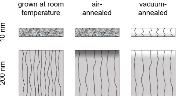
Figure 6.Effect of annealing of 10 and 200 nm thick ITO films deposited at room temperature. The annealing was performed with a heating rate of 0.5 K/min up to 200◦C and a holding time of 1 h either in vacuum or in air. Curved lines indicate grain boundaries and fill colour the oxygen concentration. The filling style of the as-grown 10 nm thick sample indicates an amorphous structure.
3.3. Effect of Al2O3deposition
239
X-ray photoelectron spectra of 20 and 200 nm thick ITO films deposited at room temperature
240
before and after 5 ALD cycles of Al2O3, corresponding to an Al2O3thickness of 0.5 nm, are shown in
241
Fig.7. The binding energies of the uncoated 20 nm thick film are higher than those of the uncoated
242
200 nm thick film. This corresponds well with the higher carrier concentration of the thinner film
243
discussed in section3.1. The deposition of Al2O3results in the appearance of Al 2p and Al 2s emissions
244
(not shown) and a reduction of the intensities of the In 3d core level and the valence band emission.
245
After Al2O3deposition, the O 1s line exhibits a pronounced additional emission at a binding energy
246
of∼ 532 eV, which can be assigned to oxygen in the Al2O3layer. In agreement to previous work
247
[32], where Al2O3films were grown by ALD onto ITO films deposited at 400◦C, the binding energies
248
of the ITO substrate are increased by the Al2O3deposition. This corresponds to a rise of the Fermi
249
energy and indicates the formation of a surface electron accumulation layer. Such layers have been
250
frequently reported to be present at In2O3surfaces [43–46]. We like to point out that no accumulation
251
layer is present on the as-deposited surfaces, as the samples have not been exposed to air before XPS
252
measurement [6].
253
The upward shift of the Fermi energy after Al2O3 deposition can partially be assigned to a
254
reduction of the substrate, which is indicated for the 20 nm thick film in Fig.7by the appearance of
255
a shoulder on the low binding energy side of the In 3d emission (indicated by an asterisk in Fig.7)
256
and by the increased band gap emission in the valence band spectrum. However, the Fermi energy in
257
the Al2O3films deposited by the low-pressure process in our system is reproducibly pinned at 4.5 eV
258
above the valence band maximum, independent on substrate [31,32,47,48]. Together with a very small
259
valence band offset between ITO and Al2O3in the absence of pinning [32], it is expected that the Fermi
260
energy in the ITO also raises toEF−EVB >4 eV. The binding energies of the ITO substrate do not
261
correspond to such high Fermi energies but only toEF−EVB ≈ 3.3 eV. This is likely explained by
262
the formation of a very narrow space charge region at the surface of the highly doped ITO, which is
263
narrower than the depth probed by XPS. The situation corresponds to an effective modification of the
264
band alignment [32].
265
Conductivity and Hall effect measurements performed on ITO films deposited at room
266
temperature are shown in Fig. 8together with those obtained after Al2O3 deposition. Data for
Figure 7.In3d (a), O1s (b) and valence band (c) X-ray photoelectron spectra of 20 nm (solid black lines) and 200 nm (dashed red lines) thick ITO films before (bottom) and after (top) deposition of Al2O3using 5 ALD cycles. The asterisk indicates a shoulder in the In 3d spectrum, which corresponds to a partial reduction of In.
Figure 8. Hall effect measurements as a function of film thickness of ITO films deposited at room temperature (black circles), ITO films deposited at room temperature after Al2O3deposition, and ITO films deposited at room temperature after annealing in the ALD chamber (ALD-anneal) in vacuum at 200◦C. The data of the as-deposited films are the same as those in Fig.2. Dashed lines are a guide to the eye.
uncoated samples are the same as those shown in Fig.2. After Al2O3deposition, the conductivity of
268
the films is lower/higher than without Al2O3for films thinner/thicker than∼15 nm. This behaviour
269
is contradictory to defect modulation doping, which has been shown to increase the conductivity for
270
10 nm thick SnO2films [31]. As modulation doping should affect only the near interface region, no
271
substantial change of electrical properties has to be expected for thicker films.
272
The carrier concentration is increased by Al2O3 deposition, independent on film thickness in
273
accordance with the raise of the Fermi level. The highest carrier concentrations ofn≈8×1020cm−3
274
are obtained for 20 and 25 nm thick films. It is the increase of carrier concentration, which explains the
275
increase of conductivity by Al2O3deposition for films thicker than 15 nm. For films thinner than 15 nm,
276
the reduction of conductivity by Al2O3deposition is caused by a significant lowering of the mobility.
277
The Al2O3deposition is performed in vacuum chamber at 200◦C and involves heating of the
278
samples in vacuum before exposure to the process gas. As indicated by the results described in section
279
3.2, the heating process in vacuum strongly affects the electrical properties. To discriminate between
280
the effects of annealing and Al2O3deposition, additional samples were annealed in the ALD chamber
281
under the conditions present during the ALD process, just without exposure to TMA and H2O. This
annealing, which is referred to as ALD-anneal here, is shorter than the one performed in the Hall effect
283
setup. Conductivity and Hall effect measurements performed after the ALD-anneal are also shown in
284
the Fig.8.
285
The dependence of carrier concentration on film thickness after the ALD anneal is comparable to
286
the behaviour described in section3.2. Except for the 200 nm thick film, the carrier concentrations of
287
thicker films are 1020cm−3. For thinner films values of up to 8×1020cm−3are reached. This behaviour
288
has been explained in section3.2by grain growth and, for the thinner films, by donor activation and
289
oxygen extraction. Up to an ITO thickness of 50 nm, the carrier concentrations of the ALD-annealed
290
samples and of those coated with Al2O3are the same within the experimental uncertainty. This again
291
rules out the presence of modulation doping. For films thicker than 50 nm, the Al2O3-coated films
292
exhibit higher carrier concentrations than the ALD-annealed ones. Apparently, the exposure to Al2O3
293
is more reducing than vacuum alone, in agreement with the partial reduction of the films observed by
294
XPS.
295
Al2O3deposition results in a strong reduction of mobility for samples with thickness<50 nm.
296
This reduction is not related to the high temperature but must be caused by the ALD process. It is
297
probably related to the chemical reduction of the film, which is indicated by XPS in Fig.7. The strong
298
reduction of the film might increase grain boundary potential barriers, which have been related to
299
reduced Sn (Sn+II) at the grain boundaries [19]. Extraction of oxygen from grain boundaries would
300
then increase the density of trapping centers and increase the potential barrier height. As the effect
301
will be restricted to the surface region due to the limited diffusivity of oxygen at 200◦C, the observed
302
increase of mobility of the Al2O3coated films with ITO thickness is reasonable.
303
The absence of a modulation doping effect upon Al2O3 deposition, which has been clearly
304
demonstrated for SnO2 [31] and which may also contribute to the formation of two-dimensional
305
electron gases at SrTiO3interfaces with Al2O3[49,50], is very likely related to the high mobility of
306
defect species. The annealing experiments discussed in section3.2clearly demonstrate that oxygen
307
defects are sufficiently mobile to diffuse several nanometers during processing at the Al2O3deposition
308
temperature of 200◦C. The compensating oxygen interstitial defects will then diffuse towards the
309
interface to screen the potential difference induced by the high Fermi energy at the interface [51]. The
310
condition required to enable defect modulation doping, which is the kinetic suppression of equilibrium
311
concentrations, is not met with ITO at 200◦C. Lower processing temperatures for ALD deposition,
312
which has been demonstrated in literature [52,53], would be required.
313
4. Summary and Conclusions 314
Low-temperature processed ITO thin films offer the potential of overcoming the doping limit by
315
suppressing the equilibrium of compensating oxygen interstitial defects. The aim of this work was to
316
provide a more detailed understanding of the processes, which determine the carrier concentrations
317
of ITO films processed at substrate temperature where oxygen diffusion and cation segregation is
318
suppressed. For this purpose, electrical properties of Sn-doped In2O3(ITO) thin films as a function
319
of film thickness have been presented and discussed. Films deposited at room temperature exhibit
320
significantly lower conductivities compared to films deposited at 200 and 400◦C. The differences are
321
caused by different carrier concentrations, while the mobilities are rather insensitive on deposition
322
temperature and film thickness.
323
Only the thinnest films deposited in our setup at room temperature are amorphous. The intensity
324
of diffraction peaks increases with increasing film thickness, which has been assigned to a slow
325
increase of substrate temperature with deposition time and to ion bombardment effects. The carrier
326
concentration of the room temperature deposited films decreases with film thickness. As the carrier
327
mobility is not affected by the reduced carrier concentration, which would be expected for grain
328
boundary scattering, the reduction of n is explained by the formation of very small grains with
329
overlapping space charge regions.
Room temperature deposited 10 nm thick amorphous and 200 nm thick crystalline films have
331
been annealed in vacuum and air at 200◦C. Conductivity and Hall effect measurements were recorded
332
during the complete annealing cycles. The thicker films exhibit a slight increase in carrier concentration
333
and reduction of mobility during annealing, regardless of the annealing atmosphere. The changes can
334
be explained by grain growth. A change of effective doping concentration by variation of the oxygen
335
content can be excluded. This is consistent with previous experiments and calculations on oxygen
336
diffusivity. A change of oxygen content is, however, evident for the 10 nm thick films. Annealing in
337
vacuum results in a substantial increase of carrier concentration by almost an order of magnitude to
338
n >1021cm−3, while annealing in air results in a decrease of carrier concentration. It is noted that
339
annealing in air does, in contrast to annealing in vacuum, not lead to crystallization of the 10 nm thick
340
films.
341
During annealing at 200◦C, diffusion of oxygen does therefore only affect a very thin region near
342
the surface of thicker films. Manipulating the carrier concentrations in thicker films is therefore not
343
an option at this temperature. The remaining diffusivity of compensating oxygen defects at 200◦C is,
344
however, sufficient to screen the high Fermi level induced by deposition of Al2O3using atomic layer
345
deposition. This disables the use of defect modulation doping at this temperature. But, the growth of
346
Al2O3at lower substrate temperatures remains an option.
347
Apart from the fact that defect modulation doping at lower temperatures cannot be ruled out at
348
present, it does not seem possible to achieve carrier concentrations approaching those observed with
349
the electrochemical reduction technique by post-deposition treatments. A realization of such carrier
350
concentrations using a suitable deposition at low-substrate temperature appears more realistic. With
351
such a process, the inherently small grain size of low-temperature grown films has to be overcome, as
352
this clearly limits carrier concentrations. The use of seed layers, such as the recently demonstrated
353
Fe2O3might be a solution for this [27].
354
Author Contributions:Thin film deposition, electrical and XPS analysis was performed by G K D, X-ray diffraction 355
by H R and J B and additional conductivity measurements by J H. Discussion and interpretation of results was 356
conducted by G K D, D B and A K. The Manuscript was written by and G K D and A K and revised by all authors; 357
Funding has been acquired by D B and A K. 358
Funding: This work was carried out in the framework of EJD-FunMat (European Joint Doctorate for 359
Multifunctional Materials) and has received funding from the European Union’s Horizon 2020 research and 360
innovation programme under the Marie Sklodowska-Curie grant agreement No 641640. 361
Acknowledgments:The authors acknowledge the Consortium des Moyens Technologiques Communs (CMTC) -362
Grenoble INP platform for diffraction characterization equipment. 363
Conflicts of Interest:The authors declare no conflict of interest. The founding sponsors had no role in the design 364
of the study; in the collection, analyses, or interpretation of data; in the writing of the manuscript, and in the 365
decision to publish the results. 366
Abbreviations 367
The following abbreviations are used in this manuscript: 368
369
ALD atomic-layer-deposition ITO Sn-doped In2O3
XPS X-ray photoelectron spectroscopy XRD X-ray diffraction
370
References 371
1. Ginley, D.S.; Hosono, H.; Paine, D.C., Eds. Handbook of Transparent Conductors; Springer: New York, 2010. 372
2. Ellmer, K. Past achievements and future challenges in the development of optically transparent electrodes. 373
Nature Photonics2012,6, 809–817. 374
3. Battaglia, C.; Cuevas, A.; Wolf, S.D. High-efficiency crystalline silicon solar cells: status and perspectives. 375
4. So, F.; Kido, J.; Burrows, P. Organic Light-Emitting Devices for Solid-State Lighting. MRS Bull. 2008, 377
33, 663–669. 378
5. Riedl, T.; Gorrn, P.; Kowalsky, W. Transparent Electronics for See-Through AMOLED Displays.J. Display 379
Technol.2009,5, 501–508. 380
6. Klein, A. Transparent Conducting Oxides: Electronic Structure – Property Relationship from Photoelectron 381
Spectroscopy with in-situ Sample Preparation. J. Am. Ceram. Soc.2013,96, 331–345. 382
7. Tahar, R.B.H.; Ban, T.; Ohya, Y.; Takahashi, Y. Tin doped indium oxide thin films: Electrical properties. J. 383
Appl. Phys.1998,83, 2631–2645. 384
8. Walukiewicz, W. Intrinsic limitations to the doping of wide-gap semiconductors. Physica B2001, 385
302-303, 123–134. 386
9. Robertson, J.; Clark, S.J. Limits to doping in oxides.Phys. Rev. B2011,83, 075205. 387
10. Lany, S.; Zunger, A. Dopability, Intrinsic Conductivity, and Nonstoichiometry of Transparent Conducting 388
Oxides. Phys. Rev. Lett.2007,98, 045501. 389
11. Frank, G.; Köstlin, H. Electrical Properties and Defect Model of Tin-Doped Indium Oxide Layers. Appl. 390
Phys. A1982,27, 197–206. 391
12. González, G.B.; Mason, T.O.; Quintana, J.P.; Warschkow, O.; Ellis, D.E.; Hwang, J.H.; Hodges, J.P. Defect 392
structure studies of bulk and nano-indium-tin oxide. J. Appl. Phys.2004,96, 3912–3920. 393
13. Yamada, N.; Yasui, I.; Shigesato, Y.; Li, H.; Ujihira, Y.; Nomura, K. Doping Mechanisms of Sn in In2O3 394
Powder Studied Using119Sn Mössbauer Spectroscopy and X-Ray Diffraction. Jpn. J. Appl. Phys.1999, 395
38, 2856–2862. 396
14. Ágoston, P.; Erhart, P.; Klein, A.; Albe, K. Geometry, electronic structure and thermodynamic stability of 397
intrinsic point defects in indium oxide.J. Phys.: Condens. Matter2009,21, 455801. 398
15. Ágoston, P.; Körber, C.; Klein, A.; Puska, M.J.; Nieminen, R.M.; Albe, K. Limits for n-type doping in In2O3 399
and SnO2: A theoretical approach by first-principles calculations using hybrid-functional methodology. J. 400
Appl. Phys.2010,108, 053511. 401
16. Gassenbauer, Y.; Schafranek, R.; Klein, A.; Zafeiratos, S.; Hävecker, M.; Knop-Gericke, A.; Schlögl, R. 402
Surface states, surface potentials and segregation at surfaces of tin-doped In2O3. Phys. Rev. B2006, 403
73, 245312. 404
17. Ágoston, P.; Albe, K. Ab initio modeling of diffusion in indium oxide. Phys. Rev. B2010,81, 195205. 405
18. Hohmann, M.V.; Wachau, A.; Klein, A. In situ Hall effect and conductivity measurements of ITO thin films. 406
Solid State Ionics2014,262, 636–639. 407
19. Frischbier, M.V.; Wardenga, H.F.; Weidner, M.; Bierwagen, O.; Jia, J.; Shigesato, Y.; Klein, A. Influence of 408
dopant species and concentration on grain boundary scattering in degenerately doped In2O3thin films. 409
Thin Solid Films2016,614, 62–68. 410
20. Song, P.K.; Akao, H.; Kamei, M.; Shigesato, Y.; Yasui, I. Preparation and Crystallization of Tin-doped and 411
Undoped Amorphous Indium Oxide Films Deposited by Sputtering. Jpn. J. Appl. Phys.1999,38, 5224. 412
21. Nunes de Carvalho, C.; Luis, A.; Lavareda, G.; Fortunato, E.; Amaral, A. Effect of thickness on the 413
properties of ITO thin films deposited by RF-PERTE on unheated, flexible, transparent substrates. Surface 414
and Coatings Technology2002,151-152, 252–256. 415
22. Kim, D.; Han, Y.; Cho, J.S.; Koh, S.K. Low temperature deposition of ITO thin films by ion beam sputtering. 416
Thin Solid Films2000,377-378, 81–86. 417
23. Hao, L.; Diao, X.; Xu, H.; Gu, B.; Wang, T. Thickness dependence of structural, electrical and optical 418
properties of indium tin oxide (ITO) films deposited on PET substrates.Appl. Surf. Sci.2008,254, 3504–3508. 419
24. Kim, S.T.; Kim, T.G.; Cho, H.; Yoon, S.J.; Kim, H.S.; Kim, J.K. Thickness Dependence of Properties of ITO 420
Films Deposited on PET Substrates.J. Nanosci. Nanotechnol.2016,16, 1852–1854. 421
25. Bellingham, J.R.; Phillips, W.A.; Adkins, C.J. Electrical and optical properties of amorphous indium oxide. 422
J. Phys.: Condens. Matter1990,2, 6207–6221. 423
26. Medvedeva, J.E.; Buchholz, D.B.; Chang, R.P.H. Recent advances in understanding the structure and 424
properties of amorphous oxide semiconductors.Adv. Electr. Mater.2017,3, 1700082. 425
27. Lohaus, C.; Steinert, C.; Deyu, G.; Brötz, J.; Jaegermann, W.; Klein, A. Enhancing electrical conductivity of 426
room temperature deposited Sn-doped In2O3thin films by hematite seed layers . Appl. Phys. Lett.2018, 427
28. Koida, T.; Ueno, Y.; Shibata, H. In2O3-Based Transparent Conducting Oxide Films with High Electron 429
Mobility Fabricated at Low Process Temperatures.phys. stat. sol. (a)2018,215, 1700506. 430
29. Koida, T.; Fujiwara, H.; Kondo, M. Hydrogen-doped In2O33 as high-mobility transparent conductive 431
oxide. Jpn. J. Appl. Phys.2007,46, L685–L687. 432
30. Koida, T.; Kondo, M.; Tsutsumi, K.; Sakaguchi, A.; Suzuki, M.; Fujiwara, H. Hydrogen-doped In2O3 433
transparent conducting oxide films prepared by solid-phase crystallization method. J. Appl. Phys.2010, 434
107. 435
31. Weidner, M.; Fuchs, A.; Bayer, T.J.M.; Rachut, K.; Schnell, P.; Deyu, G.K.; Klein, A. Defect Modulation 436
Doping. Adv. Funct. Mater.2019,29, 1807906. 437
32. Bayer, T.J.M.; Wachau, A.; Fuchs, A.; Deuermeier, J.; Klein, A. Atomic layer deposition of Al2O3onto 438
Sn-doped In2O3: Absence of self-limited adsorption during initial growth by oxygen diffusion from the 439
substrate and band offset modification by Fermi level pinning in Al2O3. Chem. Mater.2012,24, 4503–4510. 440
33. Wardenga, H.; Frischbier, M.V.; Morales-Masis, M.; Klein, A. In-situ Hall-effect monitoring of vacuum 441
annealing of In2O3:H thin films. Materials2015,8, 561–574. 442
34. Khanal, R.; Buchholz, D.B.; Chang, R.P.H.; Medvedeva, J.E. Composition-dependent structural and 443
transport properties of amorphous transparent conducting oxides.Phys. Rev. B2015,91, 205203. 444
35. Park, J.O.; Lee, J.H.; Kim, J.J.; Cho, S.H.; Cho, Y.K. Crystallization of indium tin oxide thin films prepared 445
by RF-magnetron sputtering without external heating. Thin Solid Films2005,474, 127–132. 446
36. Mattox, D.M. Particle bombardment effects on thin-film deposition: A review. J. Vac. Sci. Technol. A1989, 447
7, 1105–1114. 448
37. Seto, J.Y.W. The electrical properties of polycrystalline silicon films. J. Appl. Phys.1975,46, 5247–5254. 449
38. Ellmer, K. Electrical Properties. InTransparent Conductive Zinc Oxide; Ellmer, K.; Klein, A.; Rech, B., Eds.; 450
Springer: Berlin, 2008; pp. 35–78. 451
39. Sommer, N.; Hüpkes, J.; Rau, U. Field Emission at Grain Boundaries: Modeling the Conductivity in Highly 452
Doped Polycrystalline Semiconductors.Phys. Rev. Appl.2016,5, 024009. 453
40. Preissler, N.; Bierwagen, O.; Ramu, A.T.; Speck, J.S. Electrical transport, electrothermal transport, and 454
effective electron mass in single-crystalline In2O3films. Phys. Rev. B2013,88, 085305. 455
41. Deuermeier, J.; Wardenga, H.F.; Morasch, J.; Siol, S.; Nandy, S.; Calmeiro, T.; Martins, R.; Klein, A.; 456
Fortunato, E. Highly conductive grain boundaries in copper oxide thin films. J. Appl. Phys. 2016, 457
119, 235303. 458
42. Crank, J.The Mathematics of Diffusion; Oxford University Press: Oxford, 1975. 459
43. King, P.D.C.; Veal, T.D.; Payne, D.J.; Bourlange, A.; Egdell, R.G.; McConville, C.F. Surface Electron 460
Accumulation and the Charge Neutrality Level in In2O3. Phys. Rev. Lett.2008,101, 116808. 461
44. King, P.D.C.; Veal, T.D.; Fuchs, F.; Wang, C.Y.; Payne, D.J.; Bourlange, A.; Zhang, H.; Bell, G.R.; Cimalla, 462
V.; Ambacher, O.; Egdell, R.G.; Bechstedt, F.; McConville, C.F. Band gap, electronic structure, and surface 463
electron accumulation of cubic and rhombohedral In2O3. Phys. Rev. B2009,79, 205211. 464
45. Bierwagen, O. Indium oxide—a transparent, wide-band gap semiconductor for (opto)electronic 465
applications. Semicond. Sci. Technol.2015,30, 024001. 466
46. Berthold, T.; Rombach, J.; Stauden, T.; Polyakov, V.; Cimalla, V.; Krischok, S.; Bierwagen, O.; Himmerlich, 467
M. Consequences of plasma oxidation and vacuum annealing on the chemical properties and electron 468
accumulation of In2O3surfaces.J. Appl. Phys.2016,120, 245301. 469
47. Hillmann, S.; Rachut, K.; Bayer, T.J.M.; Li, S.; Klein, A. Application of atomic layer deposited Al2O3as 470
charge injection layer for high-permittivity dielectrics . Semicond. Sci. Technol.2015,30, 024012. 471
48. Deuermeier, J.; Bayer, T.; Yanagi, H.; Kiazadeh, A.; Martins, R.; Klein, A.; Fortunato, E. Substrate reactivity 472
as origin of Fermi level pinning at the Cu2O/ALD-Al2O3interface. Mater. Res. Expr.2016,3, 046404. 473
49. Lee, S.W.; Liu, Y.; Heo, J.; Gordon, R.G. Creation and Control of Two-Dimensional Electron Gas Using 474
Al-Based Amorphous Oxides/SrTiO3Heterostructures Grown by Atomic Layer Deposition. Nano Letters 475
2012,12, 4775–4783. 476
50. Chen, Y.Z.; Bovet, N.; Trier, F.; Christensen, D.V.; Qu, F.M.; Andersen, N.H.; Kasama, T.; Zhang, W.; 477
Giraud, R.; Dufouleur, J.; Jespersen, T.S.; Sun, J.R.; Smith, A.; Nygård, J.; Lu, L.; Büchner, B.; Shen, B.G.; 478
Linderoth, S.; Pryds, N. A high-mobility two-dimensional electron gas at the spinel/perovskite interface of 479
51. Gregori, G.; Merkle, R.; Maier, J. Ion conduction and redistribution at grain boundaries in oxide systems. 481
Prog. Mater. Sci.2017,89, 252–305. 482
52. Groner, M.D.; Fabreguette, F.H.; Elam, J.W.; George, S.M. Low-Temperature Al2O3 Atomic Layer 483
Deposition.Chem. Mater.2004,16, 639–645. 484
53. Kot, M.; Das, C.; Wang, Z.; Henkel, K.; Rouissi, Z.; Wojciechowski, K.; Snaith, H.J.; Schmeisser, D. 485
Room-Temperature Atomic Layer Deposition of Al2O3: Impact on Efficiency, Stability and Surface 486