Article
An Electronic Skin Readout System for Liquid Metal based
Flexible Resistive Sensor Array
Huan Qian ZHANG 1,ξ Jee Chin TEOH 1, ξ Jian-Feng Wu 2, Long Teng Yu 1,4, Rui-Heng Wang 2, Deleon Mark Francis 3, Chwee Teck Lim 1*
1.National University of Singapore
[email protected](HQ.Z); [email protected](JC.T); [email protected](LT.Y)
2.Southeast University
[email protected](JF.W); [email protected](RH.W)
3.FlexoSense Pte Ltd
[email protected](DM.F)
4.Microtube Technologies Pte Ltd
*Correspondence: [email protected]; Tel.:+65 65167801
Author Contributions: Huan Qian ZHANG and Jee Chin TEOH contributed equally.
Abstract - Liquid metal alloy, incorporated with microfluidic manipulation, has become a promising candidate for flexible resistive sensor array (RSA) that can imitate the functions of human skin. One advantage of RSA with shared rows and shared columns is to reduce the number of wires from M × N to M + N (rows: M and columns: N) and hence to greatly lessen the complexity and burden on the electrical system. The associated drawback is the crosstalk effect between adjacent elements during measurement. Although many literatures have reported several methods to resolve this limitation, almost all of them focus only on the high resistance value (≥100 Ω) RSA. There is a lack of detailed experimental data that addresses low resistance RSA with sensing elements below 100 Ω. Here, we aim to fill the gap of this field. We established two common RSA readout systems, i.e. zero potential methods (ZPM) (setting non-scanned-sampling-electrode zero potential (S-NSSE-ZP) and setting non-non-scanned-sampling-electrode zero potential with amplifier (S-NSSE-ZP-A)) and to compare their performances in low resistance value (≤100 Ω) RSA. For ideal resistor RSA, the measurement results show that S-NSSE-ZP has at least one time higher error than S-NSSE-ZP-A.
Keywords – Resistive sensor array, measurement error, zero potential methods, liquid metal, flexible electrical skin.
1.Introduction
Electronic skin (e-Skin) is a synthetic human skin, capable of detecting mechanical pressures of various intensities and frequencies. This emerging technology are now widely applied in medical and healthcare products, such as prosthesis, robotics, patient monitoring systems etc. [1]. On top of the demanding technical specification such as high sensitivity and quick responsiveness, e-Skin necessitates three key features that distinguishes it from other physical sensors, namely stretchability, flexibility and conformability. Soft elastomers come forth as an appealing substrate choice, based on the above-mentioned criteria.
Eutectic gallium indium (EGaIn), an alloy consisting of 75% gallium and 25% indium, is a low viscosity liquid metal at room temperature and has good electrical conductivity [2]. These unique characteristics of EGaIn accomplish the making of active components in soft sensors, which to measure strain and pressure [3-5] with varying capacitance and resistance values of EGaIn upon deformation.
Capacitive sensors have advantages of high spatial resolution and good frequency response. But they suffer from stray capacitance and field interaction when they are connected in a mesh network. Resistive sensors, on the other hand, are less susceptible to stray parameters and field interaction and hence they are favored in mesh network. One drawback of resistive sensors is lower frequency response as compared to capacitive sensors; nonetheless this limitation has negligible effect on e-Skin application as only low frequency forces come into play [6]. By encapsulating liquid metal with soft elastomers, our group has previously designed and fabricated single EGaIn based pressure sensors [7-9] with
relatively low resistance range of 10 Ω baseline (no load), up to 20 Ω with car rolling and 200 Ω with foot stomping on
it. The promising research outcome has successfully spin off two startup companies (i.e. FlexoSense Pte Ltd. and Microtube Technologies Pte Ltd.) specializing in sensing for healthcare and wearable electronics. Many of the key researches focus on alleviating the patient and healthcare system burden by realizing self-monitoring of health data, such as keeping track of foot plantar pressure in potential diabetic foot patients with the aid of flexible pressure sensing insole.
These sensors are soft, stretchable, conformable and sensitive to mechanical loading and have great potentials to be used as the building block of e-Skin. Without question, single sensor is not sufficient to duplicate the function of human skin which has densely packed mechanoreceptors with very small receptive fields. To achieve high spatial resolution, a large number of individual sensors have to be merged to form a resistive sensor array (RSA). RSA enables the increment of sensing element with minimal wire linkage and least possible burden to the electrical system. The only
major concern is the crosstalk effects resulted from adjacent idle sensors that gives rise to additional measurement error. A number of RSA readout systems have been proposed to eliminate the crosstalk effect. These approaches include
inserting diode method (IDM)[10, 11], inserting transistor method (ITM) [12] [13-15], passive integrator method (PIM) [16-18], resistance matrix approach (RMA) [19], improved RMA [37] and incidence matrix approach (IMA) [20], voltage feedback method (VFM) [21-30] and zero potential method (ZPM) [29, 31-37]. Aforementioned systems only address high resistance designs; electronic networks with low resistance below 100 Ω are often left unattended. To date only one research [24] reported a mathematical simulation from 10 Ω to 100 kΩ; nonetheless, no detailed experimental data was presented in the range of 1 Ω to 100 Ω.
The low popularity and slow research progress on low resistance network is partially attributed to the technical challenges, such as larger crosstalk effect and associated greater PCB parasite effect that are adversely affecting the system performance. In addition, majority of the mechanical sensors and actuators in the market are high resistance transducers, due to the construction materials, fabrication techniques and sensing mechanisms involved.
Unquestionably, more effort is directed to study the more ubiquitous sensor array (>100 Ω) to improve usability.
More recently, however, there has been a growing interest in the development of liquid metal based RSA along with e-Skin, which registers low resistance value and inevitably triggers large PCB parasitic effect.
Here, we compared two commonly practiced readout system (setting non-scanned-sampling-electrode zero potential (S-NSSE-ZP) and setting non-scanned-sampling-electrode zero potential with amplifier (S-NSSE-ZP-A)) in order to decrease the crosstalk of the RSA system in PCB test. We first examined the effects in low value RSA and analyzed the electrical theory of these methods. We also demonstrated the best case analysis experiments with optimum circumstances.
2.Effects in low value RSA
One of the most notable effects in low value RSA is the crosstalk from adjacent unmeasured resistors.
As shown in Figure 1, the RSA is organized in the form 3*3 array. To calculate the resistance of the target resistor
‘R22’, we require the current flowing through it and the voltage difference across the element which are denoted as ‘I22’
and ‘U22’ accordingly. ‘U22’ equals the voltage difference between the row and column wire ‘Vrow2 - Vcol2’. However,
current ‘I22’ cannot be measured directly, as ‘Icol2’ on the column wire is not equivalent to ‘I22’. The crosstalk currents
R
11R
12R
13R
21R
22R
23R
31R
32R
33V
row2V
col2I
22I
21I
11I
12I
col2U
22Figure 1. Crosstalk current of resistor array
Another drawback in low value RSA is the parasitic resistance originating from the conducting strands in the printed circuit board (PCB). A copper line with 0.254 mm width, 10 mm length and 1 oz thickness will have a resistance of 19 mΩ. It appears to be a fairly insignificant value, but it will actually contribute 1% error for a 2 Ω sensor. What should be noted is that each sensor has two end lines and crosstalk effect will magnify this parasitic effect. Totally error is further boosted by increasing the array size. Fortunately, this effect can be eliminated by using wider and thicker wires.
3.Readout circuit methods for RSA
Several methods, ZPM, VFM and IDM, have been developed to omit crosstalk effect. Based on a detailed comparative analysis [24], Liu concluded that ZPM has the best performance , as compared to VFM and IDM.
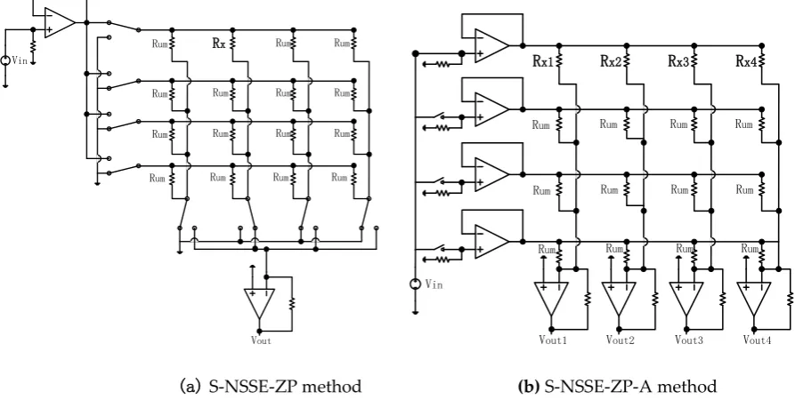
In this study, two types of ZPM are discussed, namely S-NSSE-ZP and S-NSSE-ZP-A, as shown in Figure 2. The difference between these two ZPM designs is that S-NSSE-ZP uses only one driving amplifier to run all the all rows and columns, while S-NSSE-ZP-A has one driving amplifier in each row and column. The tradeoff between circuit complexity and system performance is assessed carefully.
Rx Vin
Vout
Rum Rum Rum Rum
Rum Rum Rum Rum
Rum Rum Rum Rum
Rum Rum Rum
Vout1 Vout2 Vout3 Vout4
Vin
Rx2
Rx1 Rx3 Rx4
Rum Rum Rum Rum
Rum Rum Rum Rum
Rum Rum Rum Rum
(a)S-NSSE-ZP method (b) S-NSSE-ZP-A method
Figure 2. (a) Circuit based on the S-NSSE-ZP method (b) Circuit based on the S-NSSE-ZP-A method
For S-NSSE-ZP method, resistor 𝑅𝑥 is linked with two switches on each of its node. Two amplifiers drive resistor
𝑅𝑥 through two switches. One amplifier provides driving voltage 𝑉𝑖𝑛 on one node while the second amplifier clamps
are grounded through corresponding switches. The ideal measurement value can be calculated from Equation 1:
𝑅𝑥=
𝑉𝑖𝑛
𝐼𝑓
= − 𝑉𝑖𝑛
𝑉𝑜𝑢𝑡
× 𝑅𝑓
(1)
For S-NSSE-ZP-A method, resistor 𝑅𝑥𝑖 is linked with two amplifiers on each of its node. Resistor 𝑅𝑥𝑖 is driven by
𝑉𝑖𝑛 and grounded by two amplifiers. 𝑉𝑜𝑢𝑡𝑖 is generated by the amplifier which forces one node of 𝑅𝑥𝑖 to ground. The
other unmeasured resistors 𝑅𝑢𝑚 are grounded through connected amplifiers. The ideal measurement value can be
calculated from Equation 1 as well.
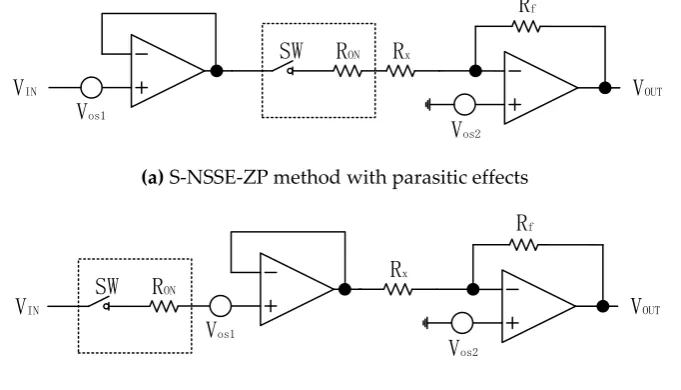
In the case of actual hardware system, two parasitic effects need to be included into the ideal equation, the switch ON resistor 𝑅𝑂𝑁 and amplifier offset voltage 𝑉𝑂𝑆, as shown in Figure 2.
V
os1V
os2R
fR
xR
ONSW
V
INV
OUT(a) S-NSSE-ZP method with parasitic effects
V
os1V
os2R
fR
xV
INV
OUTR
ONSW
(b) S-NSSE-ZP-A method with parasitic effects
Figure 2. Circuit designs that include parasitic effects in the cases of (a) S-NSSE-ZP and (b) S-NSSE-ZP-A methods
Consequently, the actual measured resistance in Equation 1 has to be modified and the equations are depicted in Equation 2:
𝑅𝑥= − (
𝑉𝑖𝑛− 𝑉𝑂𝑆1− 𝑉𝑂𝑆2
𝑉𝑜𝑢𝑡
× 𝑅𝑓+ 𝑅𝑂𝑁)
(2-1)
𝑅𝑥= − (
𝑉𝑖𝑛− 𝑉𝑂𝑆1− 𝑉𝑂𝑆2
𝑉𝑜𝑢𝑡
× 𝑅𝑓)
(2-2)
The major difference between the above mentioned two methods is that S-NSSE-ZP-A method is capable of eliminating the parasitic effect of 𝑅𝑂𝑁 with the use of amplifiers in each row and column, whereas S-NSSE-ZP does not.
However, Figure 2 is just a simplified model without crosstalk effect, which is different from the more practical applications and scenarios such as sensors array in e-Skin, whereby crosstalk is not negligible (Figure 3).
Figure 3 shows an example of 2*2 RSA with the crosstalk effect. In order to include parasitic effect of 𝑅𝑂𝑁 in this
R
ONSW
RON
SW
Vos1
V
INR
11R
12R
22R21
Vos2
V
OUTRON
RON
SW
SW
R
fFigure 3. 2×2 array circuit model including parasitic effects and crosstalk effect for S-NSSE-ZP method
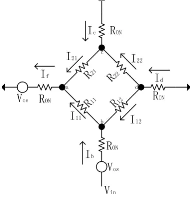
In order to calculate the existing crosstalk effect, we extract the array network and apply Kirchhoff Laws to analyze the network, as shown in Figure 4 and Equation 3.
Vos
Vos
Vin
R
ONRON
RON
RON
a d
c
b
I
bI
fId
Ic
I11
I
22I12
I21
Figure 4. Array network extracted and analyzed with Kirchhoff law
𝑉𝑎= 𝑉𝑜𝑠+ 𝐼𝑓∙ 𝑅𝑂𝑁 = 𝑉𝑜𝑠+ (𝐼21+ 𝐼11) ∙ 𝑅𝑂𝑁 (3 − 1)
𝑉𝑏= 𝑉𝑜𝑠+ 𝑉𝑖𝑛− 𝐼𝑏∙ 𝑅𝑂𝑁 = 𝑉𝑜𝑠+ 𝑉𝑖𝑛− (𝐼12+ 𝐼11) ∙ 𝑅𝑂𝑁 (3 − 2)
𝑉𝑐 = −𝐼𝑐∙ 𝑅𝑂𝑁 = −(𝐼21+ 𝐼22) ∙ 𝑅𝑂𝑁 (3 − 3)
𝑉𝑑= −𝐼𝑑∙ 𝑅𝑂𝑁 = (𝐼12+ 𝐼22) ∙ 𝑅𝑂𝑁 (3 − 4)
𝑉𝑏− 𝑉𝑎= 𝐼11∙ 𝑅11 (3 − 5)
𝑉𝑐− 𝑉𝑎= 𝐼21∙ 𝑅21 (3 − 6)
𝑉𝑏− 𝑉𝑑= 𝐼12∙ 𝑅12 (3 − 7)
𝑉𝑐− 𝑉𝑑= 𝐼22∙ 𝑅22 (3 − 8)
We hypothesize that 𝑅11= 𝑅𝑥 and 𝑅12= 𝑅21= 𝑅22= 𝑅 and 10 ∙ 𝑅𝑂𝑁< 𝑅 ≈ 𝑅𝑥. After substituting (1, 2, 3,
3-4) to (3-5, 3-6, 3-7, 3-8), we obtain Equation 4.
𝐼11(𝑅𝑥+ 2𝑅𝑂𝑁) + 𝐼12𝑅𝑂𝑁+ 𝐼21𝑅𝑂𝑁+ 𝐼22∙ 0 = 𝑉𝑖𝑛 (4 − 1)
𝐼11𝑅𝑂𝑁+ 𝐼12∙ 0 + 𝐼21(𝑅 + 2𝑅𝑂𝑁) + 𝐼22𝑅𝑂𝑁= −𝑉𝑜𝑠 (4 − 2)
𝐼11𝑅𝑂𝑁+ 𝐼12(𝑅 + 2𝑅𝑂𝑁) + 𝐼21∙ 0 + 𝐼22𝑅𝑂𝑁 = 𝑉𝑜𝑠+ 𝑉𝑖𝑛 (4 − 3)
Equation 4 is a nonhomogeneous linear equation R ∙ I = 𝑉 and it can be written as Equation 5.
(
𝑅𝑥+ 2𝑅𝑂𝑁
𝑅𝑂𝑁
𝑅𝑂𝑁
𝑅𝑂𝑁
0
𝑅 + 2𝑅𝑂𝑁
0 𝑅𝑂𝑁
𝑅𝑂𝑁
𝑅 + 2𝑅𝑂𝑁
0 𝑅𝑂𝑁
0 𝑅𝑂𝑁
𝑅𝑂𝑁
𝑅 + 2𝑅𝑂𝑁
| 𝑉𝑖𝑛 −𝑉𝑜𝑠 𝑉𝑜𝑠+ 𝑉𝑖𝑛 0 ) (5)
We define 𝑅 + 2𝑅𝑂𝑁= 𝑅+ and 𝑅𝑥+ 2𝑅𝑂𝑁= 𝑅𝑥+, then we have:
( 𝑅𝑥+ 𝑅𝑂𝑁 𝑅𝑂𝑁 𝑅𝑂𝑁 0 𝑅+
0 𝑅𝑂𝑁
𝑅𝑂𝑁 𝑅+ 0 𝑅𝑂𝑁 0 𝑅𝑂𝑁 𝑅𝑅𝑂𝑁 + | 𝑉𝑖𝑛 −𝑉𝑜𝑠 𝑉𝑜𝑠+ 𝑉𝑖𝑛 0 ) (6)
After rearranging, we have: ( 1 1 0 0 0 1 0 1 0 𝑅+⁄𝑅𝑂𝑁 −1 1 −𝑅+⁄𝑅𝑥+ 1 0 𝑅+⁄𝑅𝑂𝑁 | 𝑉𝑖𝑛⁄𝑅𝑥+ −𝑉𝑜𝑠⁄𝑅𝑂𝑁
(2𝑉𝑜𝑠+ 𝑉𝑖𝑛) 𝑅⁄ +
0
)
(7)
Rearranging row 2 and 3, we have:
( 1 0 0 0 0 0 0 1 0 𝑅+⁄𝑅𝑂𝑁 −2 1 −𝑅+⁄𝑅𝑥+
1 + 𝑅+⁄𝑅𝑥+
− 𝑅+⁄𝑅𝑂𝑁
𝑅+⁄𝑅𝑂𝑁
||
𝑉𝑖𝑛⁄𝑅𝑥+
−𝑉𝑜𝑠⁄𝑅𝑂𝑁− 𝑉𝑖𝑛⁄𝑅𝑥+
(2𝑉𝑜𝑠+ 𝑉𝑖𝑛) 𝑅⁄ +
0 )
(8)
Rearranging row 3, we have:
( 1 0 0 0 0 0 0 1 0 𝑅+⁄𝑅𝑂𝑁 0 1 −𝑅+⁄𝑅𝑥+
1 + 𝑅+⁄𝑅𝑥+
1 𝑅+⁄𝑅𝑂𝑁
|
𝑉𝑖𝑛⁄𝑅𝑥+
−𝑉𝑜𝑠⁄𝑅𝑂𝑁− 𝑉𝑖𝑛⁄𝑅𝑥+
− 𝑉𝑖𝑛𝑅𝑂𝑁𝑅𝑥⁄2𝑅+2𝑅𝑥+
0
)
(9)
Rearranging row 1, we have:
( 1 0 0 0 0 0 0 1 0 𝑅+⁄𝑅𝑂𝑁 0 1 0 1 + 𝑅+⁄𝑅𝑥+
1 𝑅+⁄𝑅𝑂𝑁
|
𝑉𝑖𝑛(2𝑅𝑥+𝑅+− 𝑅𝑂𝑁𝑅𝑥) 2𝑅⁄ 𝑥+2𝑅+
−𝑉𝑜𝑠⁄𝑅𝑂𝑁− 𝑉𝑖𝑛⁄𝑅𝑥+
− 𝑉𝑖𝑛𝑅𝑂𝑁𝑅𝑥⁄2𝑅+2𝑅𝑥+
0 )
(10)
Rearranging row 2, we have:
( 1 0 0 0 0 0 0 1 0 1 0 1 0 0 1 0 |
𝑉𝑖𝑛(2𝑅𝑥+𝑅+− 𝑅𝑂𝑁𝑅𝑥) 2𝑅⁄ 𝑥+2𝑅+
−𝑉𝑜𝑠⁄𝑅+− 𝑉𝑖𝑛𝑅𝑂𝑁(2𝑅𝑥+𝑅+2− 𝑅𝑥𝑅𝑂𝑁𝑅𝑥+− 𝑅𝑥𝑅+𝑅𝑂𝑁) 2𝑅⁄ 𝑥+2𝑅+3
− 𝑉𝑖𝑛𝑅𝑂𝑁𝑅𝑥⁄2𝑅+2𝑅𝑥+
− 𝑉𝑖𝑛𝑅𝑥⁄2𝑅+𝑅𝑥+ )
(11)
Rearranging row 2, row 3 and row 4 again, we have:
( 1 0 0 0 1 0 0 0 0 0 1 0 0 0 0 1 |
𝑉𝑖𝑛(2𝑅𝑥+𝑅+− 𝑅𝑂𝑁𝑅𝑥) 2𝑅⁄ 𝑥+2𝑅+
− 𝑉𝑖𝑛𝑅𝑥⁄2𝑅+𝑅𝑥++𝑉𝑜𝑠⁄𝑅++ 𝑉𝑖𝑛𝑅𝑂𝑁(2𝑅𝑥+𝑅+2− 𝑅𝑥𝑅𝑂𝑁𝑅𝑥+− 𝑅𝑥𝑅+𝑅𝑂𝑁) 2𝑅⁄ 𝑥+2𝑅+3
−𝑉𝑜𝑠⁄𝑅+− 𝑉𝑖𝑛𝑅𝑂𝑁(2𝑅𝑥+𝑅+2− 𝑅𝑥𝑅𝑂𝑁𝑅𝑥+− 𝑅𝑥𝑅+𝑅𝑂𝑁) 2𝑅⁄ 𝑥+2𝑅+3
− 𝑉𝑖𝑛𝑅𝑂𝑁𝑅𝑥⁄2𝑅+2𝑅𝑥+ )
(12)
From (3-1), we have 𝐼𝑓= 𝐼21+ 𝐼11. From (12) row 1 (𝐼11) and 3 (𝐼21), we have:
𝐼𝑓= −𝑉𝑜𝑠⁄𝑅+− 𝑉𝑖𝑛𝑅𝑂𝑁(2𝑅𝑥+𝑅+2− 𝑅𝑥𝑅𝑂𝑁𝑅𝑥+− 𝑅𝑥𝑅+𝑅𝑂𝑁) 2𝑅⁄ 𝑥+2𝑅+3+ 𝑉𝑖𝑛(2𝑅𝑥+𝑅+− 𝑅𝑂𝑁𝑅𝑥) 2𝑅⁄ 𝑥+2𝑅+ (13)
After simplifying, we have:
𝐼𝑓 =
−3𝑅𝑂𝑁𝑅𝑥+ 2𝑅𝑥𝑅 + 4(𝑅 + 𝑅𝑥)𝑅𝑂𝑁
2𝑅𝑥2𝑅 + 4𝑅𝑂𝑁(𝑅𝑥2+ 2𝑅𝑅𝑥)
𝑉𝑖𝑛−
𝑉𝑜𝑠
𝑅 + 2𝑅𝑂𝑁
(14)
We can evaluate 𝐼𝑓from Equation (14) by assuming 𝑅𝑂𝑁 and 𝑉𝑜𝑠 equal to zero (ideal case), then 𝐼𝑓 = 𝑉𝑖𝑛
matches equation (1).
Even though Equation (14) is derived from S-NSSE-ZP method, it can also be applied in the case of S-NSSE-ZP-A given that 𝑅𝑂𝑁= 0, as shown in Equation (15):
𝐼𝑓 =
𝑉𝑖𝑛
𝑅𝑥
−𝑉𝑜𝑠 𝑅
(15)
and it matches Equation (2-2).
From Equation (1), we know for S-NSSE-ZP method:
𝑉𝑜𝑢𝑡= −𝐼𝑓× 𝑅𝑓 = −
−3𝑅𝑂𝑁𝑅𝑥+ 2𝑅𝑥𝑅 + 4(𝑅 + 𝑅𝑥)𝑅𝑂𝑁
2𝑅𝑥2𝑅 + 4𝑅𝑂𝑁(𝑅𝑥2+ 2𝑅𝑅𝑥)
𝑉𝑖𝑛𝑅𝑓+
𝑉𝑜𝑠𝑅𝑓
𝑅 + 2𝑅𝑂𝑁
(16)
And we know for S-NSSE-ZP-A method:
𝑉𝑜𝑢𝑡= −𝐼𝑓× 𝑅𝑓= −
−3𝑅𝑂𝑁𝑅𝑥+ 2𝑅𝑥𝑅 + 4(𝑅 + 𝑅𝑥)𝑅𝑂𝑁
2𝑅𝑥2𝑅 + 4𝑅𝑂𝑁(𝑅𝑥2+ 2𝑅𝑅𝑥)
𝑉𝑖𝑛𝑅𝑓+
𝑉𝑜𝑠𝑅𝑓
𝑅 + 2𝑅𝑂𝑁
−𝑉𝑜𝑠𝑅𝑓 𝑅
(17)
4.Best-case Circuit Analysis
In this section, best-case circuits are examined. Various experiments have been designed to evaluate the performances of the S-NSSE-ZP method and the S-NSSE-ZP-A method under optimum circumstances, with varying parameters such as switch resistor value (𝑅𝑂𝑁), array size (𝑆𝐴𝑅), unmeasured array resistors value (𝑅𝑢𝑚) and measured
resistor value (𝑅𝑥).
The output amplifier’s voltage of an ideal single resistor is represented as 𝑉𝑖𝑑. Meanwhile, the output amplifier’s
voltage of array resistors is measured as 𝑉𝑎𝑟𝑟. The measurement error between them are evaluated as follows:
𝑒% =𝑉𝑖𝑑− 𝑉𝑎𝑟𝑟 𝑉𝑖𝑑
× 100 (18)
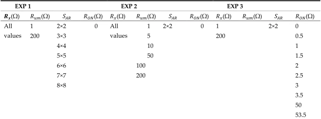
The number of possible outcomes, from the combination of the selected 4 varying parameters, is too large to be studied. Many of these combinations are less useful and lack practical application. To optimize the experiment effort and outcome, only sets of experiments (EXP) with carefully chosen combinations are analyzed (Table 1). The switches resistances (𝑅𝑂𝑁) of S-NSSE-ZP have several value such as: 0.5Ω, 1 Ω, 1.5 Ω, 2 Ω, 2.5 Ω, 3 Ω, 3.5 Ω, 50 Ωand 53.5 Ω. The
array size (𝑆𝐴𝑅) is in the range of 2×2, 3×3, 4×4, 5×5, 6×6, 7×7 and 8×8. The unmeasured array resistors values (𝑅𝑢𝑚) are 1
Ω, 5 Ω, 10 Ω, 50 Ω, 100 Ωand 200 Ω. The measured resistor values (𝑅𝑥) are: 1 Ω to 10 Ω with 1 Ω each step, 19 Ω to 20 Ω
with 1 Ω each step, 20 Ω to 100 Ω with 10 Ω each step, 100 Ω to 200 Ω with 10 Ω each step.
Table 1. Experiments with selected combinations
EXP 1 EXP 2 EXP 3
𝑹𝒙(Ω) 𝑅𝑢𝑚(Ω) 𝑆𝐴𝑅 𝑅𝑂𝑁(Ω) 𝑅𝑥(Ω) 𝑅𝑢𝑚(Ω) 𝑆𝐴𝑅 𝑅𝑂𝑁(Ω) 𝑅𝑥(Ω) 𝑅𝑢𝑚(Ω) 𝑆𝐴𝑅 𝑅𝑂𝑁(Ω)
All values
1 2×2 0 All values
1 2×2 0 1 2×2 0
200 3×3 5 200 0.5
4×4 10 1
5×5 50 1.5
6×6 100 2
7×7 200 2.5
8×8 3
3.5 50 53.5 EXP 1 analyzed the effect of array size 𝑆𝐴𝑅 on 𝑒% with the best state of switch resistor 𝑅𝑂𝑁 and the worst/best
states of unmeasured array resistors 𝑅𝑢𝑚.
EXP 2 analyzed the effect of unmeasured array resistors 𝑅𝑢𝑚 on 𝑒% with the best state of switch resistor 𝑅𝑂𝑁 and
the best state of array size 𝑆𝐴𝑅.
worst/best state of unmeasured array resistors 𝑅𝑢𝑚 and measured resistor 𝑅𝑥.
The best and the worst states refer the minimum and the maximum 𝑒% in (16) and (17).
The two parallel connected amplifiers used in S-NSSE-ZP method are OPA197, because of its low 𝑉𝑜𝑠 (100uV) and
relatively high output current (65mA). High output current is important for S-NSSE-ZP circuit design, as the whole array is driven by only one amplifier. It is difficult to find one single suitable amplifier that owns these two characteristics, as high drive ability and low 𝑉𝑜𝑠 are opposite in nature and cannot be satisfied simultaneously. In order
to increase the driving ability without raising 𝑉𝑜𝑠, we used two parallel connected amplifiers. The switches used in
S-NSSE-ZP method are TS3A24159, because of its low ON state resistance (0.3 Ω).
Meanwhile in S-NSSE-ZP-A design, the amplifiers used are OPA4388, because of their low 𝑉𝑜𝑠 (2.25μV). The
switches are ADG804, due to the low ON state resistor (0.5 Ω). However, it is not a critical parameter for this method. Because of the power supply requirement of OPA197 and OPA4388, S-NSSE-ZP and S-NSSE-ZP-A are supplied with 3.3V and 2.5V power sources respectively.
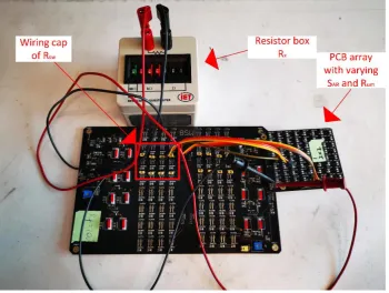
The experimental setup is shown in Figure 5. We can change 𝑅𝑠𝑤 of S-NSSE-ZP by plugging in/out the wiring cap
of the experimental resistors. Different 𝑆𝐴𝑅 and 𝑅𝑢𝑚 are realized by using PCB arrays with varying 𝑆𝐴𝑅and 𝑅𝑢𝑚
value. The value of 𝑅𝑥 is adjusted by the resistor box. Figure 5 is the hardware experimental system.
Figure 5. Experimental setup for S-NSSE-ZP and S-NSSE-ZP-A design (only S-NSSE-ZP is shown)
5.Results and Discussion
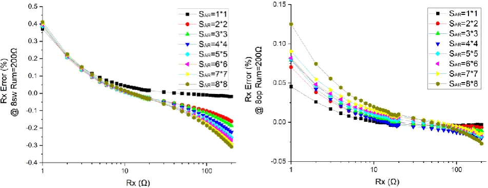
S-NSSE-ZP method is labeled as 8sw in the result graphs, as 1 amplifier and 8 switches are used to drive the array resistors arranged in rows or columns. S-NSSE-ZP-A method is named as 8op, as 8 amplifiers are adopted.
Figure 6 shows the error in S-NSSE-ZP and S-NSSE-ZP-A method when 𝑅𝑢𝑚 is 200 Ω and 𝑆𝐴𝑅changes from 1*1 to
Figure 6. The effect of 𝑅𝑥 on measurement error of different 𝑆𝐴𝑅 when 𝑅𝑢𝑚= 200Ω in ZP and
S-NSSE-ZP-A method.
Figure 7 shows the error in S-NSSE-ZP and S-NSSE-ZP-A method when 𝑅𝑢𝑚 is 1 Ω and 𝑆𝐴𝑅changes from 1×1 to
8×8.
Figure 7. The effect of 𝑅𝑥 on measurement error of different 𝑆𝐴𝑅 when 𝑅𝑢𝑚= 1Ω in S-NSSE-ZP and
S-NSSE-ZP-A method.
Figure 8 shows the error in S-NSSE-ZP and S-NSSE-ZP-A method when 𝑆𝐴𝑅= 2 × 2 and 𝑅𝑢𝑚 changes from 1 Ω to
200 Ω.
Figure 8. The effect of 𝑅𝑥 on measurement error of different 𝑅𝑢𝑚 when 𝑆𝐴𝑅= 2 × 2 in ZP and
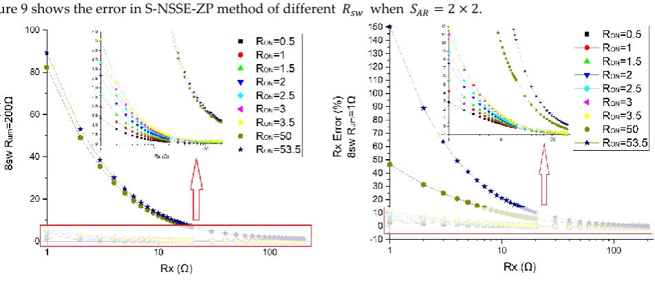
Figure 9 shows the error in S-NSSE-ZP method of different 𝑅𝑠𝑤 when 𝑆𝐴𝑅= 2 × 2.
Figure 9. The effect of 𝑅𝑥 on measurement error of different 𝑅𝑠𝑤 when 𝑆𝐴𝑅= 2 × 2.
As shown in Fig. 6, the error of 8sw is twice higher than 8op. That is because 8sw is restricted by 𝑅𝑠𝑤 and amplifier
driving ability.
In Fig. 6, when the 𝑅𝑥 is increasing from 1Ω to 100Ω, both errors of 8sw and 8op will decrease quickly. This is
because the effect of connect wire parasitic resistor and PCB trace resistor will decrease with increasing 𝑅𝑥.
Also, when 𝑅𝑥 is larger than 100 Ω, the error will increase again. We think it is the result of the real hardware
limitation. As shown in Fig. 2, the output amplifier has a feedback resistor which is 100 Ω in our design. If the 𝑅𝑥 is
more than 100 Ω, the gain of amplifier will be less than 1. As the 𝑉𝑖𝑛= 10 𝑚𝑉, so the 𝑉𝑜𝑢𝑡 will be less than 10mV. We
can rewrite equation (2-1) as equation (18). When 𝑉𝑜𝑢𝑡 is decreasing, the middle term in the right side of equation (18)
will increase and the error effect of 𝑉𝑂𝑆1 and 𝑉𝑂𝑆2 will also increase. So the totally error will increase.
𝑅𝑥 = − (
𝑉𝑖𝑛
𝑉𝑜𝑢𝑡× 𝑅𝑓−
𝑉𝑂𝑆1+𝑉𝑂𝑆2
𝑉𝑜𝑢𝑡 × 𝑅𝑓+ 𝑅𝑂𝑁) (18)
A more common way to explain this phenomenon is that 𝑉𝑜𝑢𝑡 is limited in a small range when gain is less than 1.
The effect of 𝑉𝑂𝑆 will increase with decreasing 𝑉𝑜𝑢𝑡.
In Fig. 6, the array size change leads to a monotonic change in error.
As shown in Fig. 7, the error of 8sw and 8op is much higher than in Fig. 6. This is because 𝑅𝑢𝑚 changed from 200
Ω in Fig. 6 to 1 Ω in Fig. 7. The smaller 𝑅𝑢𝑚 needs the larger driving ability, which is limited by the amplifier feature.
In Fig. 7, we can see the errors converge to a negative value instead of zero. That is because the simple equation (2) cannot match the real system when 𝑅𝑢𝑚 decreases to 1 Ω. The crosstalk effect is the dominant error now. We should
use equations (16) and (17) which are derived from crosstalk effect to analyze this phenomenon. The last term in the right side of equation (16) and (17) is a constant, so that it will form an offset after the first item converge to its minimum.
In Fig. 7, the array size change leads to a monotonic change in error.
In Fig. 8, we can see the error of 8sw is higher than 8op. This is because 8op has 8 separated amplifiers and each one of them has enough driving ability to force one column or row resistors, but 8sw has only one amplifier and its driving ability is not enough for the whole array of resistors.
We can see the error converge to an offset value when 𝑅𝑥 increases as well. With increasing 𝑅𝑢𝑚, the offset value
will decrease. This can be proven by the last term in the right side of equation (17) and (18) as well.
In Fig. 9, we can see the error of 8sw increases with 𝑅𝑠𝑤. There is a negative convergent offset when 𝑅𝑢𝑚= 1 and
zero convergent offset when 𝑅𝑢𝑚= 200. Both can be proven by equations (16) and (17). As the last term in equation
(16) and (17) is divided by R which is rewritten as 𝑅𝑢𝑚 here, thus the larger 𝑅𝑢𝑚 leads to the smaller offset.
From the above analysis, we can make some suggestions in the design of an actual hardware system to measure low value RSA.
• Decreasing the connection wire, PCB trace and switch resistor.
• Decreasing the offset voltage of all amplifiers and making sure their offset voltage is equalized to zero.
• Decreasing the array size and separating large array to several independent small arrays.
• As the power cost increases greatly with array size, it is not recommended to use this circuit design in battery driven wearable system, especially without any low power design.
• S-NSSE-ZP-A method has lower error than S-NSSE-ZP method, because this method bypasses the switch resistor and has enough amplifier current driving ability.
6.Conclusions
References
1. Chortos, A., J. Liu, and Z. Bao, Pursuing prosthetic electronic skin.Nature materials, 2016. 15(9): p. 937.
2. Dickey, M.D., Stretchable and soft electronics using liquid metals.Advanced Materials, 2017. 29(27): p. 1606425.
3. Cheng, S. and Z. Wu, A Microfluidic, Reversibly Stretchable, Large‐Area Wireless Strain Sensor.Advanced Functional Materials, 2011. 21(12): p. 2282-2290.
4. Roberts, P., et al. Soft-matter capacitive sensor for measuring shear and pressure deformation. in 2013 IEEE International Conference on Robotics and Automation. 2013. IEEE.
5. Vogt, D.M., Y.-L. Park, and R.J. Wood, Design and characterization of a soft multi-axis force sensor using embedded microfluidic channels.IEEE sensors Journal, 2013. 13(10): p. 4056-4064.
6. Tiwana, M.I., S.J. Redmond, and N.H. Lovell, A review of tactile sensing technologies with applications in biomedical engineering.Sensors and Actuators A: physical, 2012. 179: p. 17-31.
7. Yeo, J.C., et al., Wearable tactile sensor based on flexible microfluidics.Lab on a chip, 2016. 16(17): p. 3244-3250. 8. Yeo, J.C., et al., Triple-state liquid-based microfluidic tactile sensor with high flexibility, durability, and sensitivity.Acs
Sensors, 2016. 1(5): p. 543-551.
9. Yu, L., et al., Highly stretchable, weavable, and washable piezoresistive microfiber sensors.ACS applied materials & interfaces, 2018. 10(15): p. 12773-12780.
10. Snyder, W.E. and J.S. Clair, Conductive elastomers as sensor for industrial parts handling equipment.J IEEE Transactions on Instrumentation
Measurement, 1978. 27(1): p. 94-99.
11. Prutchi, D. and M. Arcan, Dynamic contact stress analysis using a compliant sensor array.Measurement, 1993. 11(3): p. 197-210.
12. Tanaka, A., et al., Infrared focal plane array incorporating silicon IC process compatible bolometer.IEEE transactions on Electron Devices, 1996. 43(11): p. 1844-1850.
13. Takei, K., et al., Nanowire active-matrix circuitry for low-voltage macroscale artificial skin.Nature materials, 2010. 9(10): p. 821.
14. Wang, C., et al., User-interactive electronic skin for instantaneous pressure visualization.Nature materials, 2013. 12(10): p. 899.
15. Kane, B.J., M.R. Cutkosky, and G.T. Kovacs, A traction stress sensor array for use in high-resolution robotic tactile imaging. Journal of microelectromechanical systems, 2000. 9(4): p. 425-434.
16. Vidal-Verdú, F., et al., Three realizations and comparison of hardware for piezoresistive tactile sensors.Sensors, 2011.
11(3): p. 3249-3266.
17. Oballe-Peinado, Ó., et al., Accuracy and resolution analysis of a direct resistive sensor array to FPGA interface.Sensors, 2016. 16(2): p. 181.
18. Oballe-Peinado, Ó., et al., Improved circuits with capacitive feedback for readout resistive sensor arrays.Sensors, 2016.
16(2): p. 149.
19. Shu, L., X. Tao, and D.D. Feng, A new approach for readout of resistive sensor arrays for wearable electronic applications. IEEE Sensors Journal, 2014. 15(1): p. 442-452.
20. Lorussi, F., et al., Wearable, redundant fabric-based sensor arrays for reconstruction of body segment posture.IEEE sensors Journal, 2004. 4(6): p. 807-818.
21. Tise, B. A compact high resolution piezoresistive digital tactile sensor. in Proceedings. 1988 IEEE International Conference on Robotics and Automation. 1988. IEEE.
22. Speeter, T.H. Flexible, piezoresitive touch sensing array. in Optics, Illumination, and Image Sensing for Machine Vision III. 1989. International Society for Optics and Photonics.
23. Speeter, T.H., A tactile sensing system for robotic manipulation.The International Journal of Robotics Research, 1990. 9(6): p. 25-36.
24. Liu, H., et al., Measurement errors in the scanning of resistive sensor arrays.Sensors Actuators A: Physical, 2010. 163(1): p. 198-204.
25. D'Alessio, T., Measurement errors in the scanning of piezoresistive sensors arrays.Sensors Actuators A: Physical, 1999.
26. Wu, J., et al., A small size device using temperature sensor array.Chin. J. Sens. Actuators, 2011. 24(11): p. 1649-1652. 27. Wu, J., L. Wang, and J. Li, Design and crosstalk error analysis of the circuit for the 2-D networked resistive sensor array.
IEEE Sensors Journal, 2014. 15(2): p. 1020-1026.
28. Wu, J., et al., A novel crosstalk suppression method of the 2-D networked resistive sensor array.Sensors, 2014. 14(7): p. 12816-12827.
29. Wu, J., et al., Cable crosstalk suppression with two-wire voltage feedback method for resistive sensor array.Sensors, 2016.
16(2): p. 253.
30. Wu, J., L. Wang, and J. Li, General voltage feedback circuit model in the two-dimensional networked resistive sensor array. Journal of Sensors, 2015. 2015.
31. Lazzarini, R., R. Magni, and P. Dario. A tactile array sensor layered in an artificial skin. in Proceedings 1995 IEEE/RSJ International Conference on Intelligent Robots and Systems. Human Robot Interaction and Cooperative Robots. 1995. IEEE. 32. Saxena, R.S., et al., Virtual ground technique for crosstalk suppression in networked resistive sensors.IEEE Sensors Journal,
2010. 11(2): p. 432-433.
33. Yarahmadi, R., A. Safarpour, and R. Lotfi, An improved-accuracy approach for readout of large-array resistive sensors.IEEE Sensors Journal, 2015. 16(1): p. 210-215.
34. Wu, J. and L. Wang, Cable crosstalk suppression in resistive sensor array with 2-wire S-NSDE-EP method.Journal of Sensors, 2016. 2016.
35. Kim, J.-S., D.-Y. Kwon, and B.-D. Choi, High-accuracy, compact scanning method and circuit for resistive sensor arrays. Sensors, 2016. 16(2): p. 155.
36. Wu, J., et al., A novel two-wire fast readout approach for suppressing cable crosstalk in a tactile resistive sensor array. Sensors, 2016. 16(5): p. 720.