IJEDR1801133
International Journal of Engineering Development and Research (
www.ijedr.org
)
771
Real time Image Processing and hardware
implementation on FPGA using VHDL
Aayushi Jain, Sunil Shah
M Tech (Embedded System and VLSI Design), Deptt of Electronics and Communication Gyan Ganga Institute of Science and Technology, Jabalpur
________________________________________________________________________________________________________
Abstract - We present in this work an image component labeler-and feature extraction module that can operate in
real-time. Connected component labeling may be used as a relatively fast method to detect and extract features from images containing relatively homogeneous pixel values in a gray scale setting. This labeler is suitable for smart cameras and Field Programmable Gate Arrays (FPGA). We show in our work how complex gray value features of image components can be calculated in parallel with label assignment without first resolving complex chains of merged labels. By isolating region in “blobs” of accepted regions. The blobs may have their data extracted and further analyzed to aid in verification of which extracted blob matches features sought by the user. In this paper we present a prototype application that implements connected component labeling .The labeler and a simple counter of number of image components are implemented on a Xilinx Virtex II Pro. We report device usage, maximum frequency and power dissipation.
________________________________________________________________________________________________________
Introduction
An image processing algorithm implemented in an embedded platform is known as embedded image processing. There are two types of embedded image processing systems. Hardware and software based. Hard ware embedded systems are relatively faster and mostly designed using an FPGA. Since FPGA’s are reconfigurable, the same flexibility to that of a software based embedded system with an improved speed can be achieved, but at the expense of increased cost and difficulty level in system design. In the context of identifying “interesting” elements in an image feature detection and extraction are widely used techniques in the areas of image processing and computer vision. The volume of image data in many domains is increasing significantly and having automated features tend to be fairly complex to implement or require special libraries. Connected component labeling provides a relatively easy to comprehend and implement solution for feature detection and extraction. The required algorithm was implemented in parallel on a field programmable gate array (FPGA) which is connected to the image sensor of the camera. Only relevant information is passed on since the pixel stream is processed inside the camera and, real-time measurements with high frame rates are feasible. From raw pixel data acquisition, to the final calculation of the objects’ characteristics, all necessary steps are done in a single pass without the need of storing the image. In order to achieve a high frame rate for high-speed imaging a scalable parallel architecture for feature extraction based on connected component labeling (CCL) was developed. Thus the resulting hardware architecture ensures high performance with low memory usage and the ability to acquire the objects’ features in a single pass. Contrary to classical connected component labeling algorithms, where the image has to be scanned at least two times, the proposed approach is able to perform the processing in only a single pass. Therefore the amount of memory required for this algorithm is not as high as for storing a full image, and can therefore be reduced by one order of magnitude to only a single image row.
Due to the memory reduction, it is possible to dispense with external memory. This is an important requirement in order to accomplish an efficient implementation on FPGAs. The application of common single pass algorithms to hardware resources on FPGAs often lead to low processing speeds of one pixel per cycle, at best. Therefore, a scalable parallel memory-efficient algorithm for connected component labeling is used to counteract that effect and improve the performance. Compared with other parallel connected component labeling algorithms, the used algorithm reduces the memory requirements of the underlying hardware architecture, by a factor 100 or more for common image sizes. In comparison to other architectures, this method increases the possible number of simultaneously processed image slices. A processing throughput of4.5GPixel can be achieved on mid-range PGAs. Furthermore, the architecture is suitable for stream processing, a necessary feature for real-time image and video processing.
Real-time System
A real-time system[1] is one in which the response to an event must occur within a time limit, otherwise the system is considered to have failed. From an Image processing perspective, a realtime imaging system is one that acquires images, processes those image to produce some results, nd then utilize this results for further processing. The response to the event should occur with in the specified time. The examples are Robot vision system, in which captured images will be analyzed to find out obstacles in its path.
Serial Vs Parallel Processing
IJEDR1801133
International Journal of Engineering Development and Research (
www.ijedr.org
)
772
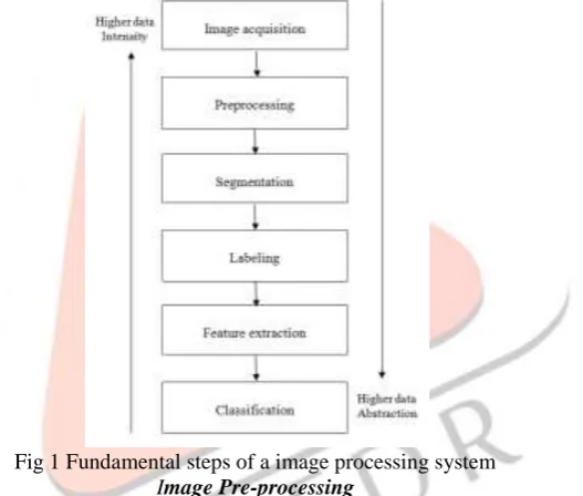
Information with regards to recognized objects in the camera’s observation area can then be transmitted through the camera’s output using, typically a low bandwidth. As typical reactive systems, such as robot navigation or surveillance of industrial processes, demand a high frame speed and low latency, it is necessary for there to be highly parallelized hardware architecture in order to provide rapid computation of image component features. Field Programmable Gate Arrays (FPGAs) are thus chosen as the preferred computation platform as they possess massive parallelism, on chip memories and arithmetic units.Fig 1 Fundamental steps of a image processing system Image Pre-processing
To obtain the clean binary image, the background intensity level of the grayscale image was found first by taking the maximum of the values of the four corner points of the trimmed image (at least one of the corner points is always be a part of the background). After finding the background level (b), a 5x5 moving window was scanned over the trimmed image, and the mean (m) and standard deviation (s) of the pixels inside the window were computed at every pixel position. If m was less than 0.7b or s was larger than 0.3m, then the pixel was considered to be a pixel of the body and was assigned a value 1. In order to clean up the spots inside the body, a morphological closing operator (binary dilation followed by erosion) was applied [7]. Next, the sequential algorithm for component labeling was used to remove unwanted isolated objects [8]. The connected components were labeled by scanning the image in x and y directions sequentially, and the largest component was selected to guarantee that there will be only one object, the body, in the binary image.
Hardware Architecture
This section describes the hardware architecture for image component labeling and feature extraction being proposed as suitable for implementation on an FPGA. Image component labeling assigns unique labels to different image components in an image as described in Section 1. Pixels are assigned labels at 𝑃5, based on the neighboring labels in 𝑃6 to 𝑃9 as shown in Figure 4(a).Adelay line of one FIFO-buffer and two registers holds the recursive data dependency arising from the neighborhood of previously labeled pixels, as shown in Figure 4(c).The length of the FIFO buffer is 𝑁C-2 elements where 𝑁C equals the length of
IJEDR1801133
International Journal of Engineering Development and Research (
www.ijedr.org
)
773
Figure : (a)Neighborhood of pixels, (b) bounding Box parameters, and (c) labeling kernel and delay line.The Labeler assigns the label codes. The label pairs (A,B) are sent to the equivalence table whenever neighboring labels are found to be equal and which must thus be merged. Label merging is targeted to either Table S or T dependent on either an odd or even frame (O/E). The resolving of linked lists of labels is thus frame interleaved with labeling and label merging. When the resolver is ready, the final steps of feature extraction can be performed. This final calculation of features will require access to the resolved equivalence table.
At the same time as the labeler is assigning label codes to different component pixels, the data of that particular pixel is accumulated in the data table S or T for feature extraction. When the labels are resolved in an equivalence table, the data present for the different label codes of same image component is resolved. There are multiple instances of data tables S and T in Figure 6, which indicates the different features that are desired to be, computed for example, area, bounding box, and so forth. The architecture has no dependency on row synchronization for either assigning labels or label merging. Data required for the extraction of features accumulates in parallel with the labeling process and more Data tables can be added for additional features. In this paper the computation of three basic image component features, namely, COG, area, and bounding box has been implemented. The Centre of Gravity of an image component 𝑂 can be defined as [34]
In (1), ro. 𝑐0 are the centroid of the image object and 𝑟𝑖, 𝑐1 re a pixel belonging to the image component𝑂. (𝑟𝑖,, 𝑐𝑖) is the intensity
value of the pixels in the image component 𝑂. This intensity value can, for the simplest case, be a binary value. However, if a high sub pixel precision is desired, the bit-width for intensity should be selected to be sufficiently large such that the quantization noise is small in comparison with other noise sources [34].
The area of an image component equals the sum of the pixels it contains. The area of the image component𝑂 is given in (2), where 𝑟𝑖, 𝑐𝑖 are the indices of the pixels belonging to the image component 𝑂:
The bounding box is the minimum rectangle enclosing an object. It is parameterized by its minimum and maximum coordinates in the row and column directions, that is, coordinates of the upper left corner (ULC), and the lower right corner (LRC). An example of a bounding box is shown in Figure 4(b), where 𝑟𝑖, 𝑐𝑖 are the indices of the pixels belonging to the image component 𝑂:
LRC = max (𝑟𝑖) , max (𝑐𝑖) , ULC = min (𝑟𝑖) , min (𝑐𝑖) ,
(𝑟𝑖, 𝑐𝑖) ∈ 𝑂.
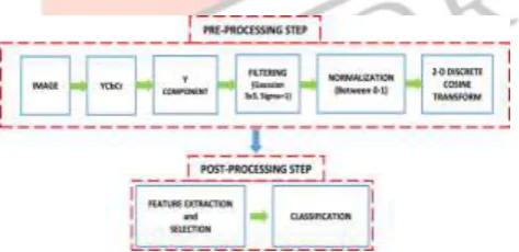
Image Enhancement Module Design Image enhancement algorithms
Underground garage lighting is relatively dark, and many of the vehicles are out of the headlights.As the result is the lights part is particularly bright displayed in the image,making the image blurred.From the gray level,the gray level focus between 0~125 and 200~255.If we use the original map directly,the part of the low gray details may be lost.So we use gray level mapping for the images of underground garage to make the dynamic gray distribution becomes uniform.A logarithmic form of compressionalgorithm can well solve such problems.Its principle is like formula (1):
t = C log(1+s) (1)
Among them: C is a scale ratio constant, t is compressed gray value,
IJEDR1801133
International Journal of Engineering Development and Research (
www.ijedr.org
)
774
Logarithmic stretch enhancement curvesThe great range of S can be converted to small range of T by using the upper type. We can conclude that from Figure ,Most of the pixels that have low gray value will focus to the high brightness section after gray mapping. Overall, it is the same time to increase the brightness of the image, the low gray value of original image has a bigger magnitude and the high gray value of original image has a smaller magnitude to achieve the effect of uniform brightness and the image details without blurring effect. Image Enhancement Module Hardware Design.
The image enhancement is mainly aimed at the luminance signal, which is the Y signal in YUV signal. De interlacing module output signals are three-way parallel YUV signal. Therefore, we must guarantee U,V two signal synchronization in the enhancement module. To this end, we set three widths of 8, the depth of 1024 FIFO by the same way before the module. Adding a detection circuit makes the three signal complete parallel conversion to serial to make the output to interface control module is single channel of 8 bit and effective image data. It can be seen that the image contrast is enhanced obviously after the ima ge enhancement module from the back of the simulation comparison chart. From Figure it can be concluded that the whole process takes 0.17 milliseconds, while the time of the software is 1.7 seconds.
Image Component Feature Calculation
IJEDR1801133
International Journal of Engineering Development and Research (
www.ijedr.org
)
775
Sequencer flow graph.After adding up the data from the different regions of the same component in the COG unit, the numerators and denominators are ready for division. After the completion of the division, a compute done signal is sent back to the Sequencer, which then enables Feature Strobe, to send the COG value to communicate to the external host. For the area and bounding box parameters, the valid data is ready after resolving the data of the same image components with different codes. The sequencer scans the equivalence table for all image objects until all objects’ features are computed and transmitted.
The key design metrics that were considered while developing the architecture for component labeling and feature extraction for real time machine vision systems are as follows:
1) high frame speed and low latency,
2) modularization, that is, a clear separation between component labeling and the extraction of different image component feature descriptors,
3) parameterize able (frame size, label code word length,etc.), 4) Low power consumption.
FPGA Area Utilization and Power Consumption
The utilization of logic cells and power consumption are two important design metrics for an FPGA based hardware system. Power simulations have been conducted for different configurations based on different label code word lengths. The hardware architecture was implemented using a Spartan-6 FPGA, which has the capacity of monitoring the power consumption on the different available voltage rails. The FPGA core is connected to the 1.2 v rail. The clock frequency for the experiments was chosen to be 27MHz.
IJEDR1801133
International Journal of Engineering Development and Research (
www.ijedr.org
)
776
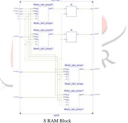
RAM BlockBoth the device utilization and power consumption for the whole architecture, as shown in Figure, are presented in Table 1. The pixel clock frequency was set to 27MHz at a frame speed of 86 frames per second. Ten bits are assigned for label codes, 34 bits are used for the numerator and 19 for the denominator in the COG calculation, and 17 bits are used for the area of each component and 10 bits for each of the bounding box parameters. The virtex5 device that was selected for implementation is based on a 45nm CMOS process, which is optimized for low power and cost.
S RAM Block
IJEDR1801133
International Journal of Engineering Development and Research (
www.ijedr.org
)
777
Device Utilization Summery
RTL View of UART
Device Utilization Summary [-]
Logic Utilization Used Available Utilization Note(s)
Number of Slice Flip Flops 83 10,944 1%
Number of 4 input LUTs 93 10,944 1%
Number of occupied Slices 80 5,472 1%
Number of Slices containing only related logic
80 80 100%
Number of Slices containing unrelated logic
0 80 0%
Total Number of 4 input LUTs 105 10,944 1%
Number of bonded IOBs 44 240 18%
Number of BUFG/BUFGCTRLs 1 32 3%
IJEDR1801133
International Journal of Engineering Development and Research (
www.ijedr.org
)
778
RTL View of Send FeatureIJEDR1801133
International Journal of Engineering Development and Research (
www.ijedr.org
)
779
Simulation WaveformsApplications and Future Scope
Any FPGA based real-time designs, that will be developed in future can be integrated in to real sim. An immediate enhancement to this simulator will be the addition of video processing features. Furthermore, edge detection algorithms like lapacian of aussian, canny edge detectors etc. will be added to the edge detection feature of the simulator. An option to compare the performance of similar image processing techniques will help the designer to choose the best implementation strategy and will make the simulator more professional. In addition, the current design can be extended to implement more complicated algorithms like viola-jones face detection algorithm, optical flow etc. These implementations has significant amount of sequential operations in the algorithms. Special strategy should be employed to mitigate the effects of communication overhead. The work presented here has wider scope and applications.
The implementation of fast face detection in a digital camera, fast object tracking, policing and interactive surveillance, and finally the applications like object tracking and chasing are some of the areas where this work can be made use of. More importantly, this work will serve as a motivation to explore the endless scopes of FPGA based computer vision designs.
References
[1.] ZHAO Peng;Hardware Design and Implementation of Real Time Image Processing System[D];Beijing University of Technology;2013.24-26;
[2.] HAN Ye;Real Time Image Processing System Based on FPGA[D];Xi'an Electronic and Science University;2014.38-40; [3.] H. Flatt, S. Blume, S.Hesselbarth, T. Sch¨unemann, and P. Pirsch, “A parallel hardware architecture for connected
component labeling based on fast label merging,” in Proceedings of the IEEE 19th International Conference on Application-Specific Systems, Architectures and Processors (ASAP ’08), pp. 144–149, July 2008.
[4.] R. C. Gonzales and R. E. Woods, Digital Image Processing, Pearson Prentice Hall, 2008.
[5.] D. G. Bailey, C. T. Johnston, and N. Ma, “Connected components analysis of streamed images,” in 2008 International
Conference on Field Programmable Logic and Applications, FPL, pp. 679–682, September 2008.
[6.] D. K. Kim, D. R. Lee, T. C. Pham, T. T. Nguyen, and J. W. Jeon, “Real-time component labeling and boundary tracing system based on FPGA,” in Proceedings of the IEEE International Conference on Robotics and Biomimetics (ROBIO ’07), pp. 189– 194, Sanya, China, December 2007.
[7.] D. Marcozzi and M. Conti, “Image processing performance analysis for low power wireless image sensors,” in Proceedings of the 5th International Workshop on Intelligent Solutions in Embedded Systems (WISES ’07), pp. 3–14, June 2007.
[8.] Z. Rasheed, G. Taylor, L. Yu et al., “Rapidly deployable video analysis sensor units for wide area surveillance,” in Proceedings of the IEEE Computer Society Conference on Computer Vision and Pattern Recognition Workshops
(CVPRW ’10), pp. 41–48, June 2010.
[9.] Jos´e, M. Farrajota, J. M. Rodrigues, and J. M. Hans du Buf, “The smart vision local navigation aid for blind and visually impaired persons,” International Journal of Digital Content Technology and its Applications, vol. 5, no. 5, pp. 362–375, 2011.
[10.] LI na;Real Time Video Image Acquisition and Storage System Based On FPGA[J];Transactions of Nanjing University of Aeronautics & Astronautics. 2012.29(4):
[11.] HUANG Tuchen;Multi Function Data Acquisition System Based On USB and FPGA [J];Atomic Energy Science and technology.2013.47(11):2172-2176.
[12.] Shen Jinsong;FPGA Co-processing Hardware and Software In Realtime Image Processing System[J];Optical Engineering;2012.39(10):143-150.