Available online: https://edupediapublications.org/journals/index.php/IJR/ P a g e | 2286
An Enhanced area efficient reconfigurable multimode interleaver
address generator for multistandard radios with low complexity
K.Satya Manuja Dept of ECE
Abstract:
Developing a reconfigurable transceiver to support multiple protocols seamlessly and efficiently is an extremely tough task. Wireless standards such as wireless local area network (IEEE 802.11a/g) and WiMAX (IEEE 802.16e) incorporate block interleaving technique to overcome the occurrence of bursterrors during transmission. Field
Programmable Gate Array (FPGA)
implementation of floor and modulus (MOD) functions to perform the two step permutation for attaining the new index is quite complex. In this study, the authors propose a low complexity and area efficient reconfigurable architecture for multimode interleaver address generator to support multiple wireless standards. In addition, a novel MOD_row and MOD_column circuit are proposed to compute MOD function for row and column counter values, respectively. The proposed address generation circuitry supports
BPSK, QPSK, 16-QAM and 64-QAM
modulation schemes under all possible code rates. The reconfigurable address generator for various block size and modulation scheme is implemented on Xilinx Spartan XC3S400 FPGA and the functionalities are verified through simulation. The synthesis results of the proposed design shows a reduction of 60% in resource utilization and an improvement of 46% in
operating frequency over the existing
approaches.
1 Introduction
Multistandard radios utilise distinct transceiver block for each wireless standard to process the corresponding communication signals. Hence, they result in increase of silicon cost and power consumption of the wireless
devices which operates on battery mode. To overcome this problem, the concept of the software defined radio (SDR) has been introduced [1]. Main aim of SDR
is to provide a single platform consisting of a hardware layer and number of software layers which incorporates set of radios from
different communication standards. The
reconfigurable nature of SDR enhances an improvement in the physical layer (PHY) of the existing and upcoming modern wireless system. Mitola [2] has introduced the concept of cognitive radio (CR) in his
dissertation. SDR based CRs are fully programmable wireless devices that can sense their environment and dynamically
adapt their transmission waveform, channels and spectrum reuse for dynamic spectrum access [1]. The wideband input signal of a
typical CR exhibits the coexistence of radio
channels based on different wireless
Available online: https://edupediapublications.org/journals/index.php/IJR/ P a g e | 2287
generator hardware needs to adapt to the different interleaving
standards. Hence, there is a scope for researchers to develop a reconfigurable architecture for address generator supporting
multiple radio standards which reduces the silicon cost. The channel interleaver is a mandatory block in the PHY of 802.11a/g and 802.16e based transmitter. A channel interleaver for multistandard SDR has to support multiple interleaving functions.
Interleaving plays a vital role in improving the performance of FEC codes in terms of bit error rate. The basic function of interleaver block is to spread the encoded data into a random one. In the conventional approach, the received data is stored row-wise in the memory and read
column-wise after applying certain
permutations. To achieve more flexibility inhe multimode
interleaver, an address generator has to be developed using specialised blocks with reconfigurable capabilities. Upadhyaya et al. [7], have implemented the conventional
interleaver on field programmable gate array (FPGA) with reduction in area. In [8], an address generating circuit, for 802.11 interleaver based on the conventional look up table (LUT) method is presented. In [9], a simple technique is developed to implement
the one dimensional interleaver equation in matrix form (2D). Khater et al. [10] carried out the hardware implementation of the address generator for 1/2 code rate WiMAX channel interleaver. Chang [11] implemented an efficient dual mode deinterleaver for both IEEE 802.16e (block deinterleaver) and outer de-interleaver for digital video broadcasting standards. Yu et al.
[12] presented a high speed block
interleaver/deinterleaver to provide arbitrary column wise permutation by adopting a low-power first in first out bank structure and a simple finite state machine (FSM). In [13], the authors have derived 2D translation of the functions for WiMAX channel deinterleaver
which is more complex for 64-QAM. Upadhyaya et al. have tested an address
generating circuit on FPGA for
WiMAXmultimode interleaver/deinterleaver in [14, 15] and WLAN multimode interleaver in [16] for all permissible code rates and modulation schemes based on FSM. Asghar, et al. [17], proposed a twofold interleaver architecture for different spatial stream application in 802.11n. Zhang et al. [18] had presented, a low complexity architecture for interleaver/ deinterleaver suitable for MIMO application in 802.11a/g/n wireless LAN. Upadhyaya et al. [19] have designed and implemented separate hardware for QPSK, 16-QAM
In this paper, we propose a
reconfigurable architecture of multimode interleaver address generator suitable for multistandard SDR by exploring the redundant hardware between different
modulation schemes. In addition, we proposed a novel MOD_row and a MOD_column circuits to compute MOD function for row and column counter values. Our work differs from the approach
[19] in the style of implementation, which eliminates the redundant hardware resources and the ROM required to store the modulus (MOD) values as well. Moreover we have derived the mathematical expression of address generator for different modulation schemes and the Boolean expression for the
MOD_column and MOD_row circuit. A detailed analysis of the proposed architecture is performed and the results are compared with
prevailing techniques which show an
improvement in terms of logic utilisation and operating frequency. The rest of the paper is organised as follows:
Available online: https://edupediapublications.org/journals/index.php/IJR/ P a g e | 2288
implementation of reconfigurable architecture for the multimode interleaver. The performance analysis of the proposed architecture is presented in Section 5. Finally, the paper is concluded in Section 6.
2 Interleaving in WLAN/WiMAX standards The wireless LAN standards 802.11a [4], 802.11g [5] and WiMAX standard 802.16e [6] supports the conventional block interleaving schemes. The channel interleaving is a process of rearranging code
symbols to reduce the effect of burst error. It processes one block of encoded bits at a time with block size equal to one OFDM
symbol depending on the modulation scheme for a specific code rate.
where, mn and kn are the first and second level permutation outputs, respectively; n represents the index of the coded bit in the
un-permutated source block which varies from 0 to (Ncbps − 1); s is the parameter defined as max (Nbpsc/2,1), where Nbpsc represents the number of coded bits per sub-carrier, that is, 1, 2, 4, 6 for
BPSK, QPSK, 16-QAM and 64-QAM, respectively [13]. d
Available online: https://edupediapublications.org/journals/index.php/IJR/ P a g e | 2290
Using (6), (9) and (12) an reconfigurable algorithm is developed to eliminate the requirement of modulo and floor function as described in Algorithm 1 (see Fig. 2).
4 Proposed reconfigurable address generator architecture
In this section, the architectural details of the proposed reconfigurable multimode interleaver address generator is presented. The architecture of the proposed reconfigurable multimode interleaver address generator for all modulation schemes is shown in Fig. 3. It comprises of a row counter, column counter, selection unit, multiplier and an adder. The output of column counter is compared with d to generate a fixed count value between 0 to d − 1. Whereas, the row counter is a variable one, which counts different levels between 0 to (Ncbps/d) − 1 based on specific block size selected by multiplexers (MUXs) M6 and M7. From (6), the hardware required
to implement BPSK and QPSK is quite similar and also the addresses are equally spaced as shown in Table 4. Whereas, the
addresses of 16-QAM and 64-QAM are not equally spaced. Therefore, the address generator has to produce two progressive
patterns for 16-QAM and three for the 64-QAM modulation scheme. Thus, the design procedure
adapted for QPSK can be extended to 16-QAM and 64-QAM with additional components such as incrementer, decrementer and a separate MOD circuit for
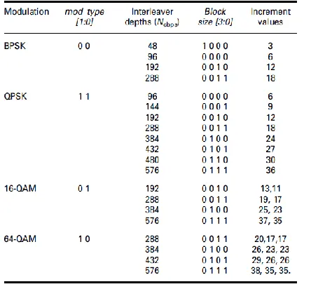
row and column counter respectively. The structure shown inside the dashed line in Fig. 3 represents the selection unit for different modulation schemes such as BPSK, QPSK, 16-QAM and 64-16-QAM block. Each modulation scheme and their corresponding block size are encoded with specific binary values as tabulated in Table 4. To ensure flexibility in generating address for different modulation schemes, MUX based logic is realised to select incremented/ decremented values of row counter based on
specific mod_type, MOD_row and
MOD_column values. The requirement of MOD functions for column and row count values in the address generation of 16-QAM and 64-QAM are satisfied by the proposed MOD_column and MOD_row circuits as shown in Figs. 4 and 5, respectively. From
Table 4, the modulation schemes can be categorised into two groups (BPSK, QPSK and 16-QAM, 64-QAM) based on the address spacing in the increment values. In hardware perspective, a simple EX-OR
gate is enough to classify the two sets of modulation schemes. The MUX M1 selects the row counter output directly if the EX-OR of mod_type is ‘0’ else it selects the incremented/decremented value of the row counter. Likewise, if the MOD_column value is ‘0’, the row counter output is directly selected in M5 for all modulation schemes as given in (6), (9) and (12). If MOD_column value is ‘1’, theMUXM3
Available online: https://edupediapublications.org/journals/index.php/IJR/ P a g e | 2291
= ‘0’ else decrement by 2. In our design, we have reduced the size of the MUXs compared with the logic in [19] by having special kind of select signal. Moreover, the
control signals are not generated externally, but generated internally from encoded binary values. 4.1 Working of MOD_column
As, the number of column (d) is chosen as 16, the column counter values goes between 0 to (d − 1), that is, maximum value of 15.
Hence, a 4-bit MOD_column circuit is proposed to compute the MOD value of column counter as shown in Fig. 4. with 4-bit input as C3, C2, C1 and C0 from MSB to LSB. The final MOD2 or MOD3 value for the column counter is obtained by performing the successive steps as shown in Table 5. 4.1.1 Logical expression for MOD_column: In general, for a 2-bit ripple carry adder with two 2-bit input numbers (B1, B0, A1, B0), that is, totally 4-bit and the outputs are 2-bit sum (Sum1, Sum0) and a carry bit (Cout). The general Boolean expression for sum and carry of a 2-bit ripple carry adder is represented as
Available online: https://edupediapublications.org/journals/index.php/IJR/ P a g e | 2292
Fig. 5 Proposed architecture of MOD_row circuit with 6-bit input
5 Performance analysis of the proposed architecture
In this section, the performance analysis of the proposed MOD
function circuit and the reconfigurable address generator with existing architectures are discussed in detail.
5.1 Mod circuit analysis and synthesis results Several implementation techniques for computing modulo function with varying input and modulo bit width on FPGA and ASIC platform are discussed in [20–22]. In [20], Sivakumar et al. discusses the implementation of X mod m architecture with the MOD values of 3, 5, 6, 7, 9 and 10 in an ASIC chip using 3 μm CMOS technology. Since, our proposed MOD circuit for address generation is implemented on FPGA, it is difficult to make a direct comparison with [20].
Available online: https://edupediapublications.org/journals/index.php/IJR/ P a g e | 2293
each stage rather than combinational logic, the design able to operate at high speed with increase in latency. The trade-off
between the complexity and latency were discussed in [21]. In [22], Gorodecky has developed a circuit for the calculation of X mod P with the Boolean expressions are represented in Reed–Muller
XOR polynomial form. It uses XOR and AND operators for the computation. For comparison of the proposed MOD circuit with [22], we have extended the logic behind our proposed MOD 3 circuit to develop a MOD 7 function with input of 10-bit width and the synthesis are performed on both Virtex 7 XC7V285t and Spartan 3 XC3S1000 FPGA. The results are tabulated in Table 10 to show its better performance in terms of LUTs and propagation
time.
5.2 Reconfigurable address generator analysis and results
The proposed reconfigurable address generator architecture is developed using Verilog HDL [23] and the functionalities are verified using Xilinx ISE. The whole design is implemented on Xilinx Spartan XC3S400 FPGA [24] device to have a better
comparison of the proposed work with the existing approaches in [15], [19].
5.2.1 FPGA simulation results: The Xilinx ISE simulation results
for Ncbps = 48-bits, 3/4 code rate, BPSK; Ncbps = 96-bits, ½ Code rate, QPSK; Ncbps = 192-bits, 1/2 code rate, 16-QAM and64-QAM modulation scheme for Ncbps = 384-bits, 2/3 code rate
5.2.2 FPGA synthesis results: In the case of FSM based
method [15], for each block size, a unique MUX is used for all modulation schemes which results in increase of hardware and
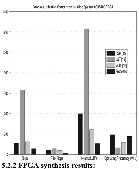
decrease in critical path delay. From Table 11, it is evident that the proposed technique shows reduction of 48% in FPGA slices, 72% in flip flops, 73% in 4-input LUT’s and with 6% lesser operating frequency compared with FSM method [15]. Compared with LUT based approach [19], our work eliminates the conventional usage
of block RAMs to house the address for each interleaver depths which results in significant reduction in slices (by 91%), in flip flops (by 81%), in 4-input LUT’s (by 91%) and the design operates at 1.85 times faster rate. Our work shows an reduction of
Available online: https://edupediapublications.org/journals/index.php/IJR/ P a g e | 2294
proposed method is shown in Fig. 7.: In the case of FSM based
method [15], for each block size, a unique MUX is used for all modulation schemes which results in increase of hardware and
decrease in critical path delay. From Table 11, it is evident that the proposed technique shows reduction of 48% in FPGA slices, 72% in flip flops, 73% in 4-input LUT’s and with 6% lesser operating frequency compared with FSM method [15]. Compared with LUT based approach [19], our work eliminates the conventional usage
of block RAMs to house the address for each interleaver depths which results in significant reduction in slices (by 91%), in flip flops (by 81%), in 4-input LUT’s (by 91%) and the design operates at 1.85 times faster rate. Our work shows an reduction of
55% in terms of logic slices, 71% in terms of flip flops and 56% in terms of 4-input LUT’s and operates at 46% faster in terms of operating speed compared with MUX based approach in [19]. For a better comparison of the implementation results, a bar chart of resource utilisation for various methods against the proposed method is shown in Fig. 7.
6 Conclusion
In this paper, a reconfigurable address generator architecture of multimode interleaver for IEEE 802.11a/g and 802.16e wireless standards supporting all possible code rates and modulation schemes has been presented. The complete hardware was developed using Verilog HDL and implemented on Xilinx Spartan 3 FPGA. In addition, a novel MOD_row and a MOD_column circuits were proposed to compute MOD function for row and
column counter values. The synthesis results of the proposed MOD circuit shows significant
reduction in resource utilisation and
improvement in operating speed compared with existing modulo
algorithms. MATLAB simulation results
endorse the functionality of the address
generator for various interleaver depths. A detailed analysis of the implementation results has been made to show the performance of the proposed method is improved compared with the existing methods. The proposed work shows an average of 60% reduction in resource utilization and an improvement of 46%
in operating frequency compared with the existing approaches. Thus, the proposed reconfigurable address generator architecture can be used to support various modulation
schemes in multimode interleaver of
multistandard SDR devices. 8 References
1 Mitola, J., Maguire, G.Q.: ‘Cognitive radio: making software radios more
personal’, IEEE Pers. Commun., 1999, 33, (4), pp. 13–18
2 Mitola, J.: ‘Cognitive radio – an integrated agent architecture for software defined
radio’. PhD thesis, Royal Institute of Technology (KTH), 2000
3 Konhauser, W.: ‘Broadband wireless access solutions–Progressive challenges and
potential value of next generation’, Wireless Pers. Common., 2006, 37, (4),
pp. 243–259
4 IEEE 802.11a: ‘Wireless LAN medium access control (MAC) and physical layer
(PHY) specifications: high-speed physical layer in the 5 GHz band’, 1999
5 IEEE 802.11g: ‘Wireless LAN medium access control (MAC) and physical layer
(PHY) specifications: further higher data rate extension in the 2.4 GHz band’, 2003
6 IEEE 802.16e: ‘Local and metropolitan networks–part 16: air interface for fixed
broadband wireless access systems’, 2005
7 Upadhyaya, B.K., Sanyal, S.K.: ‘VHDL modeling of convolutional interleaver–
deinterleaver for efficient FPGA
implementation’, Int. J. Recent Trends Eng., 2009, 2, (6), pp. 66–68
Available online: https://edupediapublications.org/journals/index.php/IJR/ P a g e | 2295
transmission on reconfigurable platforms’. Canadian Conf. on Electrical and
Computer Engineering, December 2007, pp. 801–804
9 Asghar, R., Liu, D.: ‘Low complexity multimode interleaver core for WiMAX with support for convolutional interleaving’, Int. J. Electron. Commun. Comput. Eng.,
2009, 1, (1), pp. 20–29
10 Khater, A.A., Khairy, M.M., Habib, S.E.D.: ‘Efficient FPGA implementation for
the IEEE 802.16e interleaver’. Proc. Int. Conf. Microelectron., Marrakech,
Morocco, December 2009, pp. 181–184
11 Chang, Y.N., Ding, Y.C.: ‘A low-cost dual mode de-interleaver design’. Proc Int.
Conf. Consum. Electron., Las Vegas, USA, January 2007, pp. 1–2
12 Yu, C., Yen, M.H., Hsiung, P.A.: ‘Design of a high-speed block interleaving/
deinterleaving architecture for wireless
communication applications’. Proc. Int.
Conf. Consumer Electronics, Las Vegas, USA, January 2009, pp. 1–2
13 Asghar, R., Liu, D.: ‘2D realization of WiMAX channel interleaver for efficient
hardware implementation’. Proc. World
Academy of Science and Engineering
Technology, Hong Kong, April 2009, pp. 25–29 14 Upadhyaya, B.K., Misra, I.S., Sanyal, S.K: ‘Novel design of address generator for
WiMAX multimode interleaver using FPGA based finite state machine’. Proc. 13th
Int. Conf. Computer and Information
Technology, Dhaka, Bangladesh, December 2010, pp. 153–158
15 Upadhyaya, B.K., Sanyal, S.K.: ‘Novel design of WiMAX multimode interleaver
for efficient FPGA implementation using finite state machine based address
generator’, Int. J. Commun., 2012, 6, (2), pp. 27–36
16 Upadhyaya, B.K., Sanyal, S.K.: ‘Design of a novel FSM based reconfigurable
multimode interleaver for WLAN application’. Proc. Int. Conf. on Devices and
Communications, Mesra, India, February 2011, pp. 1–5
17 Asghar, R., Dake, L.: ‘Low complexity hardware interleaver for MIMO-OFDM
based wireless LAN’. IEEE Int. Symp. on Circuits Syst. Circuits and Systems,
Taiwan, May 2009, pp. 1747–1750
18 Zhang, Z., Wu, B., Zhou, Y.M., et al.: ‘Low-complexity hardware interleaver/
deinterleaver for IEEE 802.11a/g/n WLAN’, Hindawi VLSI Design, 2012, 2012.
doi:10.1155/2012/948957
19 Upadhyaya, B.K., Sanyal, S.K.: ‘Efficient FPGA implementation of address
generator for WiMAX deinterleaver’, IEEE Trans. Circuits Syst. II, 2013, 60,
(8), pp. 492–496
20 Sivakumar, R., Dimapolos, N.J.: ‘VLSI architecture for computing X mod m’, IEE Proc. Circuit Syst., 1995, 142, (5), pp. 313–320 21 Butler, J.T., Sasao, T.: ‘Fast hardware computation of x mod z’. Proc. 18th
Reconfigurable Architectures Workshop (RAW 2011), Anchorage, Alaska, USA,
May 2011, pp. 294–267
22 Gorodecky, D.A.: ‘Reed-muller realization of X (mod P)’, CoRR, 2015, abs/
1504.04773,- arxiv.org
23 Michael, D.C.: ‘Advanced digital design with the Verilog HDL’ (Prentice-Hall,
2010, 2nd edn.)
24 Xilinx: ‘DS099 Spartan-3 FPGA family data sheet’, http://www.xilinx.com/