S
-Parameters Extraction of a Desired Network
with Time-Domain Gates
Lingyu Deng, Xiaolong Chen*, and Yajun Li
Abstract—A method for extracting a desired network from the composite measurement of a desired and undesired networks combination is proposed. The desired network is required to be a reciprocal and passive network. Time-domain responses are chosen by time-domain gates according to the signal flow diagram of the measured networks. This method can be used to characterize fixtures and de-embed of fixtures effects from the composite measurement of a device under test (DUT) and fixtures combination. This method can also compensate for masking errors. Extraction for the S-parameters of the desired network are described in detail, and the extraction result is validated with two simulations.
1. INTRODUCTION
A raw measurement obtained from a vector network analyzer (VNA) often is a composite measurement of the device under test (DUT) and the fixture. The DUT is a desired network for the measurement. The fixture has an effect on the DUT measurement and is an undesired network in the measurement. It is important to extract S-parameters of the desired network and remove the effects of the undesired network from the raw measurement. There are many methods to extract S-parameters and improve the measurement accuracy of the desired network.
The de-embedding of undesired fixtures is a common method to remove the effect of fixtures from the composite measurement of the DUT and fixtures. It is important to obtain the characterization of fixtures. Some of the characterization methods need to construct a model for a fixture [1, 2]. These models have high accuracy for simple structures and need modification with a change of frequency range. Calibration SOLT and TRL are well known [3, 4], but these need a well-designed calibration kit. A time-domain channel characterization (TCC) is also a choice to obtain the characterization of fixtures [5, 6], but the fixtures need to be symmetric.
A time-domain gate can be used to extract the desired part of the DUT [7]. Time-domain gated responses sometimes contain masking error and the masking network needs to be known to compensate for the error. Masking error occurs when the response of one discontinuity affects or obscures the response of subsequent discontinuities in the circuit.
This paper propose a method to extract the desired network S-parameters from the raw measurement by using a time-domain gate. The time-domain gate is used to choose time-domain responses according to the signal flows of the measured circuit and the S-parameters of the desired network are extracted from the time-domain gated responses. The desired network needs to be reciprocal and passive. This method can be used to compensate the masking errors and characterize the fixtures.
Received 6 May 2016, Accepted 15 June 2016, Scheduled 19 July 2016 * Corresponding author: Xiaolong Chen ([email protected]).
port 1
S
port 2 desired network
S S S S
(1) (2) (3) (4) (5)
Figure 1. A measured circuit consists of five cascading networks.
(a) (b) S S (1) (2) a b b 1 11 12 a b b 1 21 22 21
S12(1)
S(2)21 S21(3)
11
S11(4)
S12(1) S12(2) S12(3)
S21(1) S21(2) S21(3) S21(4) S21(5) S21(3) S21(4) S21(5)
S11(4) S12(3) S22(2)
Figure 2. Signal flow diagram based on the circuit of Fig. 1. (a) Signal flow diagram of reflection coefficients. (b) Signal flow diagram of transmission coefficients.
2. THEORY
The measured circuit shown in Fig. 1 is composed of five cascading networks characterized by the scattering matrices S(k). Port 1 and Port 2 are the measurement reference planes. Networks 1, 3 and 5 are transmission lines that are interrupted by discontinuities — networks 2 and 4.
Network 2 is the desired measured network and its S-parameters can’t be directly extracted from
S-parameters measured by a VNA. The algorithm for extracting S-parameters of the desired network from the raw measurements is detailed below.
2.1. Calculate the Magnitude of the S-Parameters
A signal flow diagram for the measured circuit is shown in Fig. 2. a1represents incoming waves from port
1. b11andb12 are reflected waves from different routes at port 1. Similarly,b21 andb22are transmission
waves at port 2. We can infer Eq. (1) from Fig. 2 (It is necessary to know theS-parameters dependence on frequency [8], some equations in this paper don’t include this discussion for brevity).
⎧ ⎪ ⎪ ⎪ ⎪ ⎪ ⎪ ⎪ ⎪ ⎪ ⎨ ⎪ ⎪ ⎪ ⎪ ⎪ ⎪ ⎪ ⎪ ⎪ ⎩
S11(1)=
b11
a1
=S21(1)S11(2)S12(1),
S11(2)=
b12
a1
=S21(1)S21(2)S21(3)S11(4)S12(3)S12(2)S12(1),
S21(1)=
b21
a1
=S21(1)S21(2)S21(3)S21(4)S21(5),
S21(2)=
b22
a1
=S21(1)S21(2)S21(3)S11(4)S12(3)S22(2)S21(3)S21(4)S21(5).
(1)
S(m)
ij is the scattering parameter of network m. S11(1) and S11(2) are two independent reflection
coefficients that are a part of S11. S21(1) and S21(2) are two independent transmission coefficients
that are also a part ofS21. These coefficients satisfy:
⎧ ⎪ ⎪ ⎪ ⎪ ⎨ ⎪ ⎪ ⎪ ⎪ ⎩
S11(f) =
∞
i=1
S11(i)(f),
S21(f) =
∞
i=1
S21(i)(f).
where S11(f) and S21(f) are the original measurements of the reflection and transmission coefficients
by a VNA.S11(i)(f) is a part ofS11(f), andS21(i)(f) is a part of S21(f).
In order to extract S11(i)(f) from S11(f), the reflection response s11(t) in the time domain is
calculated using the inverse Fourier transform [9]:
s11(t) = ˆF−1S11(f) = ˆF−1
∞
i=1
S11(i)(f) =
∞
i=1
s11(i)(t). (3)
ˆ
F−1is the inverse Fourier transform operation. The reflection responses
11(i)(t) corresponds toS11(i)(f).
Figure 3 shows a time domain reflection response. If the impulses of the time domain response do not overlap thens11(1)(t) can be extracted by a time-domain gate function [10]:
s11(1)(t) =s11(t) as t1 ≤t≤t2 (4)
Applying the Fourier transform, its corresponding frequency domain responseS11(1)(f) can be obtained. Repeating similar steps, it is easy to obtain S11(2)(f), S21(1)(f), and S21(2)(f). Thus Eq. (5) can be calculated based on these partialS-parameters:
S11(2)S21(1)
S11(1)S21(2)
= S (2) 12S (2) 21 S(2) 11S (2) 22 = S(2) 12 2 S(2) 11S (2) 22
=C0ejφ0. (5)
whereC0 andφ0 are the magnitude and phase of the ratio among the time-domain gatedS-parameters.
Because the desired network 2 is required to be lossless and reciprocal, itsS-parameters satisfy: ⎧
⎨ ⎩
S(2)
12 =S
(2) 21,
S(2) 11 = S
(2) 22 .
(6)
Combining Eq. (5) and Eq. (6), the amplitude of the desired networkS-parameters can be inferred: ⎧
⎨ ⎩
S(2) 11 = S
(2) 22 =
1/(1 +C0),
S(2) 12 = S
(2) 21 =
C0/(1 +C0).
(7)
1
11(1)
S (t)
11(2)
S (t)
11 S ( t ) 0 1
g (t)
t1 t2 t
Figure 3. Reflection response in the time domain.
port 2
S(3) S(4) S(5)
short
Figure 4. A short circuit that is built forθ(2)22.
2.2. Calculate the Phase of the S-Parameters
According to Eq. (5), it can be inferred:
2θ(2)12 −θ(2)11 −θ(2)22 =φ0. (8)
whereθ11(2),θ12(2), and θ22(2) are the phases ofS11(2),S12(2) and S22(2).
Network 1 is a transmission line, and its electrical length can be obtained from the time response
s11(1)(t). The phase ofS
(1)
12 can be calculated according to its electrical length. Combining the phase of
S(1)
12 and S11(1)(f), the θ
(2)
11 can be found.
12
S(3) S(4) S(5)
12 12
21
S(3) S(4) S(5)
21 21
S22 Short -1
Figure 5. Signal flow diagram for short circuit.
S_Param
Start = 0.1 GHz Step = 0.1 GHz Stop = 8 GHz Term1
Num = 1
Z = 50 Ohm
Term2 Num = 2
Z = 50 Ohm
TL1
Z = 50 Ohm
E = 360
F = 1 GHz
TL2
Z = 50 Ohm
E = 350
F = 1 GHz
TL3
Z = 50 Ohm
E = 320
F = 1 GHz
C1
C = 1.0 pF CC 2= 1.0 pF
S-PARAMETERS
Figure 6. A test circuit whereC1 is a undesired part of the measurement.
From Mason’s rule [11], we can know the relations of the short circuit S-parameters and time-domain gated responses:
SShort
22 =S22(1)−S22(2)/
S(2)
22 +S21(2)/S21(1)
. (9)
SShort
22 is the reflection parameter of the short circuit at the composite network input. TheS-parameters
S22(1)andS22(2)are time-domain gated responses and they can be extracted fromS22(f) of the measured
circuit in Fig. 1. So the phaseθ(2)22 can be inferred from S22(2):
S(2)
22 =S22(2)/(S22(1)−S22Short)−S21(2)/S21(1). (10)
θ(2)
12 can be found by combining θ (2) 11, θ
(2)
22 and Eq. (8). All the phases of network 2 S-parameters can
now be calculated.
3. EXPERIMENTAL SETUP AND RESULTS
In order to introduce the method of extracting the desired network characterization from the raw measurements, two simulation experiments are described below.
3.1. Compensate for the Masking Error
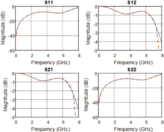
The raw measurements are theS-parameters of the DUT as shown in Fig. 6. The capacitanceC1 is an undesired network in the DUT, and its effect needs to be removed from the measurements.
0 1 2 3 4 5 6 7 8
frequency, GHz 0 5 -5 -10 -15 -20 -25 -30 -35 S , dB 11 original ideal
gate & comp gate
Figure 7. Comparison of reflection parameters from raw measurements (blue trace), time domain gated measurements (purple trace), time-domain gated and compensated measurements (green trace), and the DUT without undesired network (red trace).
(
Term1 Num = 1
Z = 50 Ohm
Term2 Num = 2
Z = 50 Ohm
Fixture 1 DUT Fixture 2
SP1
Start = 0.1 GHz Step = 0.1 GHz Stop = 8 GHz
S-PARAMETERS
(a) (b)
(c) Term1
Num = 1
Z = 50 Ohm
Term1 Num = 1
Z = 50 Ohm
Term2 Num = 2
Z = 50 Ohm
Term2 Num = 2
Z = 50 Ohm
Fixture 1 Fixture 2
Short
Fixture 1
Fixture 2 TLIN
Z = 50.0 Ohm
E = 200
F = 1 GHz
TLIN
Z = 50.0 Ohm
E = 200
F = 1 GHz
Short
TLIN
Z = 50.0 Ohm
E = 200
F = 1 GHz
1 2 2 1 1 2
1 2
Figure 9. Schematics used to extract S-parameters of two different fixtures. (a) Schematic of the through standard comprised of two fixtures. (b) Schematic of short circuit for fixture 1. (c) Schematic of short circuit for fixture 2.
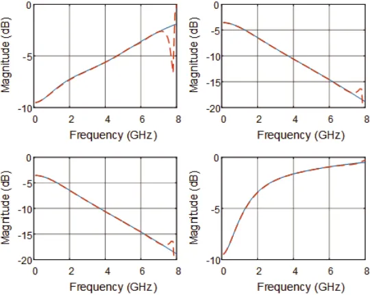
Figure 10. Comparison of fixture 1 characteristic (blue trace) with that extracted characteristic (red trace).
In order to remove the effect ofC1 from the measurements, we can use a time-domain gate to choose a time domain response related toC2 (The time domain response that is related to theC1 is removed). Because C1 represents a masking error for the time-domain gated measurements, the C1 S-parameter needs to be extracted for compensating the masking error. The extracting method described above can be used to extract the S-parameters of C1.
Figure 11. Comparison of fixture 2 characteristic (blue trace) with that extracted characteristic (red trace).
Figure 12. Comparison of original DUT characteristic (blue trace) with that de-embedding result by the method described in this paper (red trace).
3.2. De-Embedding of Two Different Fixtures
An experiment for de-embedding fixtures is introduced. The fixtures are lossless and reciprocal. The composite measurement of the DUT and two fixtures combination can be measured from the schematic shown in Fig. 8. In order to obtain the characteristics of the DUT, the fixtureS-parameters need to be obtained and the effects of the fixtures de-embedded.
A standard circuit is built as the schematics in Fig. 9 and the fixturesS-parameters can be extracted by the method described in this paper.
of the fixtures are consistent with the measurements of the fixtures.
The S-parameters of the DUT can be obtained by de-embedding the effects of the fixtures from the raw measurements. The result for the de-embedding fixtures is consistent with the measurements of the DUT. The deviation at the band edge is caused by the time domain gate.
This de-embedding experiment validates the extracting method introduced above.
4. CONCLUSION
AnS-parameters extraction method using time-domain gates is introduced. Two simulation experiments are used to validate the method. This paper discusses how to compensate for masking error or extract the characteristics of fixtures, but the key point in this paper is to introduce a new method to extract the desired network S-parameters from the original measurements by time-domain gates according to the signal flow diagram.
REFERENCES
1. Waldhoff, N., C. Andrei, D. Gloria, S. Lepilliet, F. Danneville, and G. Dambrine, “Improved characterization methology for MOSFETs up to 220 GHz,” IEEE Trans. Microwave Theory and Techniques, Vol. 57, No. 5, 1237–1243, May 2009.
2. Zhang, J., Q. B. Chen, K. Qiu, A. C. Scogna, M. Schauer, G. Romo, J. L. Drewniak, and A. Orlandi, “Design and modeling for chip-to-chip communication at 20 Gbps,” 2010 IEEE International Symposium on Electromagnetic Compatibility (EMC), 467–472, Fort Lauderdale, FL, 2010.
3. Hiebel, M., “Measurement accuracy and calibration,” Fundamental Vector Network Analysis, 5th Edition, 109–131, Rohde & Schwarz, Germany, 2011.
4. Zhang, J., Q. B. Chen, Z. Qiu, J. L. Drewniak, and A. Orlandi, “Using a single-ended TRL calibration pattern to de-embed coupled transmission lines,” IEEE International Symposium on Electromagnetic Compatibility, 197–202, Austin, 2009.
5. Dunsmore, J., N. Cheng, and Y.-X. Zhang, “Characterizations of asymmetric fixtures with a two-gate approach,” 2011 77th ARFTG Microwave Measurement Conference (ARFTG), 1–6, Baltimore, MD, 2011.
6. Adamian, V. and B. Cole, “A novel procedure for characterization of multiport high speed balanced devices,” 2006 IEEE International Symposium on Electromagnetic Compatibility, 395–398, San Jose, CA, 2007.
7. Dunsmore, J., “Time domain transforms,” Handbook of Microwave Component Measurements: With Advanced VNA Techniques, 182–192, John Wiley & Sons, New York, 2012.
8. Pozar, D. M., “Microwave network analysis,” Microwave Engineering, 4th Edition, 178–188, John Wiley & Sons, New York, 2012.
9. Chu, E., “Discrete convolution and the DFT,” Discrete and Continuous Fourier Transforms: Analysis, Applications and Fast Algorithms, 27–29, CRC Press, New York, 2008.
10. Yoon, C., M. Tsiklauri, M. Zvonkin, Q. B. Chen, A. Razmadze, A. Aflaki, K. Jingook, J. Fan, and J. L. Drewniak, “Design criteria and error sensitivity of time-domain channel characterization (TCC) for asymmetry fixture de-embedding,”IEEE Trans. Electromagnetic Compatibility, Vol. 57, No. 4, 836–846, Aug. 2015.
11. Mason, S. J., “Feedback theory — Further properties of signal flow graphs,” Proceedings of the IRE, Vol. 44, No. 7, 920–926, Jul. 1956.