University of Twente
Faculty of Electrical Engineering,
Mathematics & Computer Science
Higher Order Feedback
Loop for a Pulse Width
Modulator
Willem Stapelbroek MSc. Thesis
June 2006
Abstract
This report is about the research of a feedback loop for a Pulse Width Modulator. Different loop filters are investigated. The optimal type of loop filter depends on the types of noise in the system. In general a higher filter order of the loop-filter leads to a
better noise suppression, but there are limits. Out of this study it emerged that a 3rd
order Butterworth type filter with at 700 kHz carrier signal inserted in the last integrator is a good option for implementation. A SINAD of 112 dB in the audio band
is possible in case of 50% modulation depth. This is 29 dB better than for a 2nd order
Butterworth filter with a 350 kHz carrier signal. This last filter is used the Philips’ design which was the motive for this project. In the simulations the noise/distortion sources are jitter noise from the carrier signal, supply voltage distortion and intrinsic modulation errors. Distortion in the output stage is neglected.
Preface
In the course of the last 8 months the author of this report was engaged in his graduation (master) project. This report is a result of this project. Early October the author started his research on higher order feedback loops for Pulse Width Modulators.
The project was done in cooperation with Philips Semiconductors Nijmegen. Philips developed a good working second order feedback loop for a pulse width modulator. The initial assignment was to research if a higher order feedback loop would result in a significant better performance of the pulse width modulator. For this purpose a model was created and simulated. From the results of these simulations a loop-filter was chosen which was considered as feasible for implementation and with an optimal performance.
Next a start was made for the implementation of the loop filter. In this implementation some components were still considered as ideal or semi-ideal to simplify the analysis and to achieve a first implementation design within the time which was left for this project. The developed implementation design already gives the most important bottlenecks in order to develop an actual device.
In the monthly meetings between the author, his supervisors from the University of Twente and supervisors from Philips Semiconductors Nijmegen, many interesting discussion provided much insight in the world of pulse width modulation and feedback systems.
The author of this report likes to thank his supervisors at the University of Twente: Ronan van der Zee, Daniël Schinkel and Ed van Tuijl for their excellent guidance during this project and time for discussion which provided much insight in the field of pulse width modulation and analog designing. The author also likes tot thank his supervisors from Philips Semiconductors Nijmegen: Marco Berkhout and Arnold Freeke (at the first part of the project), who provided the project and who provide numerous of good ideas and interesting discussions.
Table of content
ABSTRACT ... 3
PREFACE ... 5
1 INTRODUCTION... 9
2 PROBLEM DESCRIPTION... 11
2.1 THE PULSE WIDTH MODULATOR...11
2.1.1 The Feed-forward Pulse Width Modulator... 11
2.1.2 The Feedback Pulse Width Modulator ... 13
2.2 2ND ORDER FEEDBACK LOOP FOR A CLASS-D AUDIO AMPLIFIER BY PHILIPS...16
2.3 PROJECT GOALS...16
3 LOOP FILTERS ... 19
3.1 LOOP FILTER CALCULATIONS AND CONDITIONS...19
3.2 BUTTERWORTH TYPE NOISE TRANSFER FUNCTION...20
3.2.1 Noise transfer function ... 20
3.2.2 Open loop transfer function... 22
3.2.3 Signal transfer function ... 24
3.3 CHEBYSHEV TYPE NOISE TRANSFER FUNCTION...25
3.3.1 Noise transfer function ... 26
3.3.2 Open loop transfer function... 27
3.3.3 Signal transfer function ... 30
3.4 LOOP FILTER CONCLUSIONS. ...30
4 SYSTEM MODEL ... 31
4.1 SYSTEM MODEL...31
4.2 IDEAL SYSTEM...32
4.3 SUPPLY VOLTAGE ERROR...32
4.4 COMPARATOR DELAY...33
4.5 PLACEMENT OF THE CARRIER SIGNAL...35
4.6 JITTER IN THE CARRIER SIGNAL...37
4.7 OUTPUT STAGE NOISE AND DISTORTION...40
4.8 700 KHZ CARRIER...41
4.9 FINAL SYSTEM MODEL SIMULATIONS AND CONCLUSIONS...43
5 FILTER IMPLEMENTATION... 45
5.1 LOOP-FILTER TOPOLOGY...45
5.1.1 Chain of Integrators with Weighted Feedforward Summation (CIFF)... 46
5.1.2 Chain of Integrators with Distributed Feedback (and Distributed Feedforward Inputs) (CIFB).. 47
5.1.3 Power dissipation of the loop-filter topologies... 48
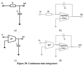
5.2 INTEGRATORS...48
5.3 FILTER IMPLEMENTATION CONCLUSIONS...50
6 LOOP-FILTER REALIZATION... 53
6.1 LOOP-FILTER TOPOLOGY...53
6.2 RCSPREAD...55
6.3 CHANGEABLE CARRIER FREQUENCY...58
6.4 THE INTEGRATOR...59
6.4.1 Miller integrator... 59
6.4.2 RHP zero cancellation... 60
6.5 VOLTAGE SWING...61
6.5.1 1st integrator:... 62
6.5.2 2nd integrator:... 63
6.5.3 3nd integrator:... 64
6.6 NOISE ANALYSIS...65
7 PARAMETER CALCULATIONS AND SYSTEM SIMULATIONS... 69
7.1 PARAMETER CALCULATIONS...69
8 CONCLUSION SUMMARY AND RECOMMENDATIONS ... 77
9 REFERENCES... 81
10 APPENDICES ... 83
10.1 BUTTERWORTH PARAMETERS...83
10.2 BUTTERWORTH CALCULATIONS...83
10.2.1 1st order ... 83
10.2.2 2nd order: ... 83
10.2.3 3rd order: ... 83
10.3 CHEBYSHEV POLYNOMIALS &STOP-BAND RIPPLE...84
10.3.1 Chebyshev polynomials ... 84
10.3.2 Stop-band ripple ... 84
10.4 CHEBYSHEV CALCULATIONS...84
10.5 CHEBYSHEV PARAMETERS...85
10.6 MATLAB/SIMULINK SIMULATION PARAMETERS...86
10.7 MATLAB/SIMULINK SIMULATION RESULTS...87
10.7.1 No noise sources... 87
10.7.2 Supply Voltage error only... 87
10.7.3 Carrier placement, no noise sources with 50% modulation depth and Butterworth type NTF... 87
10.7.4 Carrier placement, Jitter noise only with 50% modulation depth and Butterworth type NTF... 87
10.7.5 Output stage noise only with 50% modulation depth... 88
10.8 JITTER NOISE CALCULATIONS...89
10.9 OPEN LOOP CALCULATIONS...90
10.10 MILLER INTEGRATOR CALCULATIONS...91
10.10.1 Normal miller integrator ... 91
10.10.2 Zero cancellation modified miller integrator ... 92
10.11 NOISE CALCULATIONS OF AN INTEGRATOR...94
10.11.1 Resistor noise ... 94
10.11.2 Gm noise ... 94
10.11.3 Noise from the load ... 95
10.11.4 Total input referred noise voltage ... 95
1 Introduction
Pulse Width Modulators are widely used at the present day. When Pulse Width Modulators (PWM) are used as amplifier they are also called Class-D amplifiers. Class-D amplifiers have a much higher efficiency than conventional AB-amplifiers. This is the big advantage of a Class-D amplifier over a conventional AB-amplifier. This efficiency is advantageous in many ways:
- From the power consumption point of view: Because less power is lost a
device could run longer on a battery. In other words it has a longer battery life. This is very preferable in case of portable devices. Think about the various assortment of portable MP3 players, portable DVD players and of course the mobile phones nowadays.
- The amplifier will produce less heat when it has a high efficiency. Dissipated
energy in an amplifier will be converted to heat. High efficiency means less energy is dissipated and therefore less heat is produced. When less heat is produced, it is not necessary to equip the amplifier with large and bulky heat sinks. This is very attractive for car-audio. The amplifiers can be made smaller so it is easier to build in a car. Small amplifiers are also very attractive for consumer Hi-Fi.
The concept of pulse width modulation is already known for a long time, but in the early years the manufactures were not able to produce a reliable Class-D amplifier. At the present day the technology is advanced enough and today’s Class-D amplifiers equals or even exceeds the performance of conventional AB-amplifiers.
+
-+Vp
-Vp input
output filter
output stage PW
Modulator loop filter
+ +
-carrier
Figure 1: Class-D amplifier with feedback
A way to improve the performance of the Pulse Width Modulator is to equip the PWM with a feedback loop and a loop filter. This feedback loop is the main subject of this project.
Philips has already designed a good working 2nd order feedback loop for a PWM. This
First, in chapter 2 it is explained how a PWM operates, what its drawbacks are and
why a feedback loop improves the PWM. The 2nd order feedback loop developed by
Philips is quickly analyzed to develop some first ideas for design choices and to produce some reference material.
In chapter 3 the loop-filter and its effect on the performance of the PWM is analyzed in a mathematical way. Different types of loop-filters and filters with different filter orders are calculated and analyzed.
In chapter 4 the most important noise and distortion sources in a PWM are analyzed and modeled. A model for the PWM is created which includes these noise/distortion sources and the feedback loop. The different loop-filters from chapter 3 are simulated and from the results the optimal loop-filter for implementation is chosen.
Chapter 5 and 6 show the way how such a loop-filter could be implemented. The pros and cons of different implementation topologies are investigated and the best solution for implementation is determined.
2 Problem
Description
The assignment is to research and design a higher order feedback loop for a Pulse
Width Modulator (PWM). Philips developed a good-working 2nd order feedback loop
for a Class-D audio amplifier (= PWM) ([2]). It is interesting to research if a higher order feedback loop improves the PWM significantly. First let’s take a look at how a
PWM actually works and what the advantage is of a feedback loop. Next the 2nd order
feedback loop developed by Philips is discussed. This is a nice starting point and a good comparison for the simulation results of the higher order feedback system which is designed in this report. Finally the specifications and goals of the project are discussed before discussing the actual project.
2.1 The Pulse Width Modulator
The amplifier used in this project is a Class-D amplifier. The Class-D amplifiers have some advantages over the conventional AB-amplifiers. First of all they are much more efficient than AB-amplifiers. The idea behind the efficiency of a Class-D type amplifier is that, ideally, the switches and the output filter do not dissipate energy (Figure 1). Therefore the high power output stage doesn’t dissipate much energy. To start, first one should know how a Class-D amplifier or Pulse Width Modulator (PWM) works. §2.1.1 first explains the operation of the basic feed-forward PWM and gives its drawbacks. Some of those drawbacks could be eliminated by using a feedback loop. While a feedback PWM eliminates some drawbacks of the feed-forward PWM, it also has its own drawbacks. The operation and drawbacks of the feedback PWM is discussed in §2.1.2.
2.1.1 The Feed-forward Pulse Width Modulator
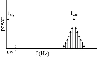
The basic idea behind the feed-forward Pulse Width Modulation is to compare the input signal with a triangle carrier-signal, this method is known as double-sided natural sampling [1]. This method is shown in Figure 2. If the comparator and the carrier signal are ideal and the modulation depth (ratio between input signal and carrier signal) is not more than 100%, the only distortion components are the harmonics of the input signal modulated around the carrier signal (Figure 3). When
choosing a carrier signal with frequency (fcar) high enough,the output can be filtered
by simple low pass filter (2nd order) to retrieve only the desired input signal.
0 0.5 1 1.5 2 2.5 3 3.5 4 4.5 5 x 10⁻⁴
time (s) input signal carrier signal PWM signal
a)
0 0.5 1 1.5 2 2.5 3 3.5 4 4.5 5 x 10⁻⁴
time (s) b)
0 0.5 1 1.5 2 2.5 3 3.5 4 4.5 5 x 10⁻⁴
time (s) c)
Figure 3: Modulation errors in a PWM
As long as the input signal has a much lower frequency as the carrier frequency, it can be considered as static. As long the input signal can be considered as quasi-static, the PWM output signal represents a time reference signal of the input signal. This is clearly visible in Figure 2, where 3 timeframes are given of situations with 3 different modulation depths. This figure is merely a raw example of how PWM works.
A model of this system is given in Figure 4.
+
-+Vp
-Vp input
output filter
output stage PW
Modulator carrier
Figure 4: Basic feedforward Class-D Model
Unfortunately in practice a PWM is not ideal. For example the supply-voltage (Vp)
will not be constant but will contain a ripple which translates into a tone at the ripple frequency harmonics due to the modulation. Due to modulation, the ripple frequency and its harmonics also folds around the input signal. Another non-ideality is clock jitter in the carrier generator. This clock jitter will corrupt the triangular carrier signal and so the comparator decision will be slightly wrong. Also dead-time used to be a source of distortion. Dead-time is the small time during the switching of the output stage, when the pull-up and pull-down transistors in the output stage are both off in order not to short-circuit the supply voltage ([2]). Due to new techniques, dead-time is not considered as a big source of distortion anymore ([3]).
Most of these distortions can be effectively suppressed by applying feedback to the system. But feedback has to be designed with care, due to the chance of instability. In
fsig fcar
BW
powe
r
the next paragraph a feedback PWM is described in more detail. But before continuing some definitions are given to ease the explanation.
- Modulation depth (Δ = Vin/Vt): the ratio between the amplitude of the input
signal (Vin) and the amplitude of the carrier signal at the input of the
comparator (Vt)
- Feedforward gain (GPWM≈ VPWM/Vt): considering only the low frequency (the
audio frequency rang in this case), the ratio between the amplitude of the output and the amplitude of the carrier signal at the input of the comparator.
2.1.2 The Feedback Pulse Width Modulator
In a feedback PWM, the output is compared with the input of the system. This way the error of the system is estimated and thus can be compensated. A loop filter needs to be inserted with the denominator at least one order higher than the nominator to avoid instability and to achieve the desired noise suppression ([5]). In chapter 3 we will see that a well designed loop filter will have low-pass characteristics for the input signal, while every signal introduced inside the feedback loop has high-pass characteristics. If the input bandwidth is low frequency, the noise and distortion introduced by for example the output stage is very low at the input frequencies (Figure 5). The noise and distortion at high frequencies are not suppressed, but these can be filtered out by a low-pass output filter. This way the noise and distortion in the filtered output signal is very low.
Figure 5: Principle of feedback noise suppression
An example of a feedback PWM is given in Figure 6. In this example the output filter is not part of the feedback system.
+
-+Vp
-Vp input
output filter
output stage PW
Modulator loop filter
+ +
-carrier
Figure 6: Basic feedback Pulse Width Modulator Model fbw
Unwanted noise before shaping
When feedback is applied this way, every source introduced inside the feedback loop will be suppressed due to the feedback loop. So as mentioned in the previous paragraph, adding feedback to a PWM will effectively decrease the non-ideality effects like the supply voltage modulation and clock jitter (in most cases).
But feedback also introduces its own distortions:
- Due to PWM modulation the input frequency and its higher harmonics are
present around multiples of the carrier frequency. For a feedforward system this is not an issue, because they are filtered out by the output filter. In case of feedback the higher harmonics fold back to the baseband creating noise/distortion components in the baseband (Figure 7).
Figure 7: Modulation errors in a PWM with feedback
- In an ideal PW modulator the input is compared with an ideal triangular carrier
signal. In the feedback system shown in Figure 6 the carrier signal is a block wave inserted at the input of the last integrator of the loop filter to create the triangular signal at the input of the comparator as will be seen in §6.1. This means the feedbacked signal is affected by the loop filter, while the carrier signal is not affected by the loop filter. Due to the loop filter the feedbacked signal will have a different phase shift than the carrier signal at the input of the comparator, thus the comparison is not ideal anymore from the ideal point of view. As will be seen in paragraph 4.5 the carrier signal can be inserted at the input of the loop-filter to get a better comparison. But this also introduces its drawbacks as will be discussed in paragraph 4.5.
- Another point of concern for feedback systems is the stability issue.
o The first logic step to avoid instability is to place the loop filter zeros
in the left halve of the s-plane. This is considered as basic knowledge.
o Another source of instability and more specific for this system, is
clipping of the PW Modulator. Clipping in this context is when, in a period of the carrier signal, the output doesn’t switch. Clipping of the
modulator occurs when the error triangle signal Ve (Figure 6) is larger
than the carrier triangle frequency Vt. One can say the system is
overloaded in this case. As explained in [2] the criterions for avoiding instability in a feedback loop are as follow:
The carrier triangle signal should be twice as big as the triangle
error signal 2
t e
V > V ( 2-1 )
fsig fcar
BW
powe
r
The unity-gain frequency should be smaller than the carrier
frequency divided by π.
car UG
ω ω
π
< ( 2-2 )
For higher order loop filters the LHP zero frequency should be
sufficiently lower than the unity-gain frequency (ωUG) in order
to obtain sufficient phase margin and acceptable peaking of the closed-loop transfer.
o Another point to avoid instability is that open loop transfer function
has a 1st order slope at the unity gain frequency. If the slope is a higher
order the NTF will have an overshoot and which can result in an instable system.
- In practice the comparator is also not ideal. The comparator suffers from a
delay which translates into an extra phase-shift. In a feedback system this affects the performance of the system. Because the input signal is low frequency, it can be considered as quasi-static. The input signal can be considered as a very slow changing signal (almost constant) with respect to the carrier signal. If the comparator delay is very small the input signal can be still considered as an almost constant value. If this is the case the comparator delay can be neglected. If the comparator delay is bigger the input signal has to be considered as less constant and so the comparison is less accurate. The result
is that the error signal (Ve) will be bigger and so it has to be taken into account
in the stability analysis.
- As mentioned in §2.1.1, clock jitter corrupts the triangular carrier signal,
which results in wrong comparator decisions. The triangular carrier signal is created by integrating a block signal ([4]). Clock jitter in the block signal not only creates a variable phase shift, but it also affects the amplitude of the triangular carrier signal from period to period (see Figure 8, in the figure the jitter is very severe in order to show its effect). Jitter causes noise in the audio bandwidth. This so called jitter noise could be suppressed by the feedback loop. It depends were the carrier signal is inserted. (This will be explained in this report). Also jitter could result in clipping of the PWM. The jitter noise will add a little voltage to the internal signal and if this is not proper analyzed, this extra voltage could cause clipping.
Next chapter will go more into the loop filter and calculate the optimum filters.
Figure 8: Carrier signal: a) ideal, b) with jitter
a) b)
2.2 2
ndorder feedback loop for a Class-D audio amplifier by
Philips
Philips has developed a good working 2nd order feedback loop for a Class-D audio
amplifier ([2]). The amplifier is realized in a silicon-on-insulator (SOI)-based technology called A-BCD. This technology allows creating low voltage and high voltage circuits on the same wafer without latch-up phenomena. This way a 60 Volt output stage could be realized on the same wafer as the 12 Volt internal circuitry. The PWM method used in this amplifier is also double-side natural sampling. This method was explained in §2.1.1. Conceptually, the input signal is compared with a triangular reference wave. When the input signal is converted to a PWM signal the output stage amplifies it to high power levels. The PWM output is then filtered by an output filter to extract only the audio content. A simple LC filter can be used for the purpose.
The amplifier uses a 2nd order feedback loop to suppress the supply voltage ripple and
pulse-shape errors in the switching power stage. As input VI-converter a Gm is chosen because it has some advantages over a resistor:
- The input impedance is independent of the feedback loop.
- It has a differential input.
- The amplifier can be muted without influencing the feedback loop
- The noise and offset of the first integrator in the loop are not amplified by the
closed-loop gain
Still the input gm and the feedback resistor have to be very linear to achieve a good closed-loop performance.
The reference triangle is realized by injecting a square-wave current into the virtual ground of the second (last) integrator. By doing this the duty-cycle errors or jitter from the oscillator is suppressed by the feedback loop. This allows one to use a less accurate oscillator.
The focus in this design was to reduce the effect of deadtime and supply-voltage modulation. This distortion is generated at the output stage. Using the feedback loop this distortion is being suppressed according to the noise transfer function.
The amplifier achieved a good result with a THD+N of 0.017% for 1 watt output power
Some terms mentioned above are maybe unknown to some readers. But these elements will be explained in the course of this report. One can also read [2] to get a basic idea.
2.3 Project Goals
System level:
- The filter type determines the shape of the noise transfer function (NTF). As
will be seen, in this report the filter is designed on the basis of the NTF (how the noise and distortion generated at the end of the feedback loop is filtered). There exist many filter types like: Butterworth, Chebyshev, Elliptic and many hybrid filters. Due to the time limit for this project the focus is reduced to only the Butterworth and Chebyshev type filter because of their flat pass-band. The best type is used for implementation.
- The filter order determines the amount of filtering. A higher order filter
results in more aggressive filtering of the noise generated inside the feedback loop. This is visible in the NTF. Higher order filters result in steeper slopes in the stop-band. The orders 1 till 5 are investigated
- The loop gain and corner frequencies are important factors for the loop
filter. First it also determines the amount of filtering. A high loop gain results in more aggressive filtering of the noise generated inside the feedback loop. But the loop gain and corner frequencies cannot be set freely. If the loop gain is chosen too big or if the corner frequencies are put on a too high frequency, the system can become unstable due to equations (2-1). In the first part of this project an optimum for the loop gain and corner frequencies is investigated. - The frequency of the carrier signal is also very important in the design of the
loop filter. The carrier frequency set restrictions to, for example, the loop gain. By increasing the carrier frequency a higher loop gain can be chosen without the system becoming unstable.
It is not possible or even advantageous to ever increasing things like the filter order or loop gain. There are optimums in these parameters. These optimums depend on
different points. The most important point is stability of the system. For example as
already mentioned before, one cannot choose the loop gain too high. This results in an unstable system.
The choices to make as mentioned above also depend on the amount and types of noise or distortion. There are big differences between how to filter different types of noise or distortion. The noise- and distortion-sources investigated in project are:
- Supply voltage error
- Carrier jitter noise
And in lesser extend:
- Output stage noise
The systems were modeled at system level in simulation software. The software used is Matlab and Simulink.
Implementation of the loop-filter:
The level of implementation depended on the available amount of time. It was not possible to develop an implementation ready for production in the given amount of time for this project.
- There exist different structures of the loop filter for the same NTF. The
differences in those structures are for example: the signal transfer function, power consumption and the specifications of the components inside. A subject of the structure of the loop filter is how the gain factors are implemented. For this implementation one can think about the trade-off between linearity and tunability
- Because the foundation of the loop filter is its integrators, the structure of the
integrators is also an important issue. At first the integrators are considered as
ideal, but in practice the integrators as far from ideal. Integrators suffer from
many non-idealities like: parasitic zeros and poles, finite gain and load
impedances. One can live with these non-idealities only when the integrator is
properly designed. The different structures of the integrators differ from each other in: linearity, frequency range, power consumption, area consumption and tunability.
The values of the components are calculated. During the calculation of the components there are some things to be taken into account:
- Voltage swing: Signals in the actual systems cannot be limitless. One limit is
the internal supply voltage. Signals cannot exceed the supply voltage. So the gain of the integrators has to be scaled in order that the signals will not clip to the supply voltage.
- It is important to place the parasitic zeros and poles on a place of desire. It
can lead to instability or the function of the filter can heavily decrease if these parasitics lie at the wrong places. By choosing the right values of the components the parasitic can be placed on a place where they do no harm. The implementation design is made in Cadence and is suitable for Philips’ ABCD3 process.
Table 1 shows the specifications used in this project. Some of the specifications are already mentioned above. Others were also given in the assignment.
Parameter Specification
Filter types Butterworth or Chebyshev
Filter order 1 t/m 5
Carrier frequency 350 kHz or 700 kHz
Input frequency range 20 Hz – 20 kHz
Input voltage 2 Volt peak-peak
Output voltage 60 Volt peak-peak Amplification = 30
Internal supply voltage 12 Volt peak-peak
Comparator delay 30 ns
Table 1: Specifications
3 Loop
filters
Feedback systems are able to improve the output signal very much in comparison to a feedforward system.
+
-+Vp
-Vp input
output filter
output stage PW
Modulator loop filter
+ +
-carrier
Figure 9: Basic feedback Pulse Width Modulator Model
With feedback it is possible to suppress noise and unwanted signals in a desired frequency range which are inserted or generated inside the feedback loop, while the input signal at these frequencies are passed through unaffected. While the noise or unwanted signals are suppressed in the signal-band, at other frequencies they are not suppressed and sometimes even amplified. This is sometimes also described as noise-shaping. If this is done the unwanted signals and noise can be filtered out of the system, without affecting the input signal. Only the unwanted signals and noise introduced inside the feedback loop can be shaped. Unwanted signals and noise inside the desired frequency band, introduced outside the feedback loop, are not seen by the feedback loop and so it is not be affected by it.
The way the noise is shaped can be determined by the loop-filter. The loop filter determines the signal transfer function (STF) and noise transfer function (NTF) of the system.
In the next chapter the different type loop filters are introduced and calculated. In this project the noise will only be suppressed as in a high-pass filter. It is possible to transfer noise from a certain pass-band, but that is not further discussed in this project.
3.1 Loop filter calculations and conditions
The loop filter can be seen as a function with zeros and poles:
( ) ( )
( )
H H Z s H s
P s
= ( 3-1 )
The open loop transfer is given by:
( )
( ) ( )
( )
H
open PWM PWM
H Z s
H s G H s G
P s
= = ( 3-2 )
( ) ( ) ( )
1 ( ) ( ) ( )
open PWM H
ST
open H PWM H
H s G Z s
H s
H s P s G Z s
= =
+ + ( 3-3 )
With GPWM as the gain of the feed-forward PWM, ZH(s) as the zeros of the loop filter
transfer and PH(s) as the poles of the loop filter transfer.
In this project the field of research is higher order filters. When the order of the loop filter is an order higher than two the calculations will become very complex very rapidly. So it becomes difficult to calculate the optimal filter. Because of the feedback loop, this PW modulator can be considered as noise-shaper. The shape of the noise spectral density is of our interest. So why not specify a certain desired noise transfer function and calculate the loop filter from that noise transfer function. (see [5])
The noise transfer function of the system is given by: ( )
1 1
( ) ( ) 1
1 ( ) ( ) ( ) ( )
H
NT open
open H PWM H NT
P s
H s H s
H s P s G Z s H s
= = ⇒ = −
+ + ( 3-4 )
Looking at equation (3-4) it can be noticed that the poles of loop filter will translate to the zeros of the noise transfer function while the poles, the zeros and the PWM gain are responsible for the poles of the noise transfer function.
To have a good noise reduction in a feedback system it’s desired that the feedback loop has a high loop gain. The loop gain will determine the amount of noise reduction. If the loop gain is high the system has more noise reduction (see equation (3-4)), while the STF stays unity (see equation (3-3))
Related to the filter design, a design constrain has to be followed. The order of the denominator of the loop filter transfer has to be higher than de numerator. This is to avoid an algebraic loop in the system ([5]). Together with equation (2-4) one can see that the order the nominator and denominator of the NTF are both the same order as the denominator of the open loop transfer. In other words, the NTF has the same amount of poles as zeros and this is the same as the amount of poles in the open loop transfer. This can be summarized to the following equation:
( )
PH order( )
ZH order(
PNTF)
order(
ZNTF)
order( )
PHorder > ⇒ = = ( 3-5 )
With this in mind the desired noise transfer can be designed. The simplest approach is to take a high-pass version of a standard filter (like a Butterworth or Chebyshev) as the base of the noise transfer function. Equation (3-4) shows how to calculate the loop filter from the noise transfer function.
In the next paragraphs two different prototypes are discussed. The Butterworth type (§3.2) and the Chebyshev type (§3.3)
3.2 Butterworth type Noise transfer function
3.2.1 Noise transfer function
A high-pass Butterworth characteristic is calculated by placing poles in the origin of the s-plane. The order of the zeros must be the same the order of the poles in order to have a flat pass-band.
2
1
( )
1
c n
c
H j ω
ω
ω ω
=
⎛ ⎞ + ⎜ ⎟ ⎝ ⎠
( 3-6 )
Where n is the order of the system and ωc is the angular cutoff frequency or the -3·n
dB point. The low-pass Butterworth transfer function will have the following form.
_ 1 1
1 1
( )
...
n c
but low n n n n
c n c c
H s
s a s a s
ω
ω − ω − ω
− =
+ + + + ( 3-7 )
The value of parameter ai can be found in appendix 10.1.
To translate it to a high-pass filter next substitution has to be applied:
c
c
ω ω
ω ⇒ ω ( 3-8 )
Using (3-6) and (3-8) the high-pass version of a Butterworth transfer function will look like this:
_ 1 1
1 1
( )
...
n
but high n n n n
c n c c
s
H s
s aω s − a ω −s ω
− =
+ + + + ( 3-9 )
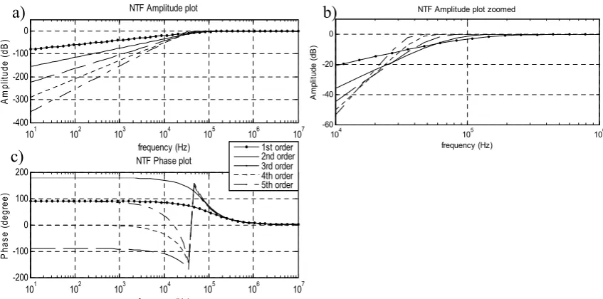
NTF’s from order 1 to 5 are calculated their bode-plots are shown in Figure 10. As can be seen from the amplitude plot, higher order filters will suppress the noise at low frequencies more than the lower order filters. But equation (2-2) has to be kept in mind. At the unity gain frequency of the open loop transfer function there has to be enough phase margin. This is why the corner frequency shifts to the left for higher filter orders. When we take a better look at the open loop filter we can see how the corner frequency is determined for every order of filter and what the actual phase margins are. This will be discussed in next paragraph.
Figure 10: Bode plots of NTF's with Butterworth characteristics: a) amplitude, b) amplitude zoomed in, c) phase
c)
104 105 106
-60 -40 -20 0
frequency (Hz)
A
m
pl
itud
e (
dB
)
NTF Amplitude plot zoomed
a) b)
101 102 103 104 105 106 107
-400 -300 -200 -100 0
frequency (Hz)
Am
pl
itu
de
(
dB)
NTF Amplitude plot
101 102 103 104 105 106 107
-200 -100 0 100 200
frequency (Hz)
P
has
e (
degr
ee
)
NTF Phase plot
3.2.2 Open loop transfer function
Now this high-pass transfer function is taken as the prototype for the NTF (3-9). With this as starting point it’s easy to calculate the open-loop transfer function using equation (3-4). The result is in following form:
1 1
1 ... 1
( ) c n n cn cn
open n
a s a s
H s
s
ω − ω − ω
−
+ + +
= ( 3-10 )
From this formula it can be seen what the loop filter has to be and with what the loop gain. From equations (3-2) and (3-10) it can be seen that for Butterworth type filter the loop gain is:
1
PWM c
G =aω ( 3-11 )
and the loop filter has to look like:
2 1 1 1 1 1 ... ( ) ( ) ( ) n n
n n c c
n a s s a a Z s H s
P s s
ω − ω −
− + + − +
= = ( 3-12 )
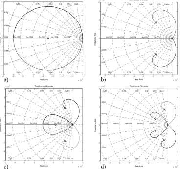
Better insight in stability can be obtained from the root locus plots (see Figure 11 for
2nd till 5th order filters). As can be seen from the formula as well from the root locus
plots of Figure 11 the poles of the open loop transfer function with Butterworth characteristics lie in the origin.
Figure 11: Root locus plots of the open loop transfer function with Butterworth characteristics for a: a) 2nd order, b) 3rd order, c) 4th order and d) 5th order loop filter
Root Locus 2nd order
Real Axis Ima gi nar y A xi s
-8 -7 -6 -5 -4 -3 -2 -1 0 x 105 -4 -3 -2 -1 0 1 2 3 4x 10
5 0.16 0.34 0.5 0.64 0.76 0.86 0.94 0.985 0.16 0.34 0.5 0.64 0.76 0.86 0.94 0.985 2e+004 4e+004 6e+004 8e+004 1e+005 +005 a) b) c) d)
Root Locus 3rd order
Real Axis Im ag in ar y A xi s
-7 -6 -5 -4 -3 -2 -1 0 x 105
-4 -3 -2 -1 0 1 2 3 4x 10
5 0.16 0.34 0.5 0.64 0.76 0.86 0.94 0.985 0.16 0.34 0.5 0.64 0.76 0.86 0.94 0.985 2e+004 4e+004 6e+004 8e+004 1e+005
Root Locus 4th order
Real Axis Im ag in ar y A xi s
-7 -6 -5 -4 -3 -2 -1 0 1 x 10⁵ -4 -3 -2 -1 0 1 2 3 4x 10
5 0.16 0.34 0.5 0.64 0.76 0.86 0.94 0.985 0.16 0.34 0.5 0.64 0.76 0.86 0.94 0.985 2e+004 4e+004 6e+004 8e+004 1e+005
-7 -6 -5 -4 -3 -2 -1 0 1 x 10⁵ -4 -3 -2 -1 0 1 2 3 4x 10
5 0.16 0.34 0.5 0.64 0.76 0.86 0.94 0.985 0.16 0.34 0.5 0.64 0.76 0.86 0.94 0.985 2e+004 4e+004 6e+004 8e+004 1e+005
Root Locus 5th order
This results in the high gain at dc level as shown in the amplitude bode plot of Figure 12a. Because the NTF is calculated as a perfect Butterworth function the open loop transfer will be a little bit deformed and shows not a perfect Butteworth filter, this is visible because the zeros in the left half plane don’t lie in line with a circle around the origin, characteristic for Butterworth. If the order is higher than 2, a too low loop gain will result in an instable feedback system. Looking at the root locus plots, some poles will travel first through the right half plane before entering left half plan. If a pole lies in the right half plane the system will be unstable.
As already mentioned the corner frequency of the desired NTF can be determined by looking at the open loop transfer function. From chapter 2.1.2 it’s known that the unity gain frequency of the feedback loop should be sufficiently lower than the carrier frequency. See equation (2-2).
A carrier frequency of 352.8 kHz is used in the simulations. 352.8 kHz is multiple of 44.1 kHz (a well-known sample frequency in audio) and thus useful for the Fourier analysis.
Using a carrier frequency of 352.8 kHz the unity gain frequency should be less than
352.8/π kHz (or 705600 rad/sec). For a 1st order system it’s easy to see that a loop
gain of 700000 satisfies this condition. As mentions in paragraph 2.1.2 the slope of
the amplitude plot has to be 1st order at the unity gain frequency. So a higher order
loop-filter needs zeros at a frequency lower than the unity gain frequency in order to
have a 1st order slope at unity gain. The frequency of the transition from higher order
slope to the open loop transfer (ωc_o) is related to the corner frequency (ωc) of the
NTF (equation (3-10)). To have the best noise suppression it is desirable to choose ωc
as high as possible. But one cannot choose the unity gain frequency from equation
(2-2) as the ωc_o. This way the -3·n dB point at ωc_o is put at this frequency and thus
the actual unity gain frequency of the system (ωUG) will be higher, which results in an
unstable system. In order to satisfy (2-2) the ωc_o have to shift a little bit to a lower
frequency.
As can be seen from equation (3-11), the PWM gain (GPWM) is directly related to ωc.
It is only multiplied by the constant a1. From appendix 10.1 it can be seen a1 increases
when the order of the filter increases. If one uses a constant GPWM and increases the
order of the filter, ωc decreases (keeping in mind the NTF has to be a ideal
Butterworth type). Because ωc_o decreases when ωc decreases, if the GPWM is held
constant, ωc_o decreases when a higher order is chosen. This is exactly what is needed.
Now look at a 1st order filter. No ωc_o is present and GPWM could be calculated using
equations (2-2) and (3-11). It turns out if this same GPWM is also used for higher order
filters, the ωc_o of these filters will be placed low enough to have a 1st order slope of
the open loop transfer at unity gain. The actual values for ωc_o are not calculated in
this project. The actual could be calculate with equation (3-12).
As can be seen in appendix 10.2.1 the loop gain of the 1st order filter is the same as
Figure 12: Bode plots of open loop transfer functions with Butterworth characteristics: a) amplitude, b) amplitude zoomed in, c) phase
Appendix 10.2 shows the Butterworth filter calculations until 3rd order filter. Higher
order filters are becoming too complex to put in this report and are easy to be calculated by Matlab. See Figure 13 for the Matlab code.
Figure 13: Matlab code: Butterworth filter calculations
In this code the function butter() returns the zeros, poles and gain for a high pass
Butterworth transfer function of n’th order and with a corner frequency of ftri/a1.
ftri is the frequency in Hz of the triangular carrier and a1 is taken from the table of
appendix 10.1 to shift the ωc_o for higher order filters. The rest of the functions
calculate the NTF, open loop transfer function and STF, but they don’t need any explanation.
3.2.3 Signal transfer function
Finally according to (3-3) the STF is:
1 1
1 1
1 1
1 1
... ( )
...
n n n
c n c c
S n n n n
c n c c
a s a s
H s
s a s a s
ω ω ω
ω ω ω
− −
−
− −
−
+ + +
=
+ + + + ( 3-13 )
Figure 14 shows the bode plots of the STF. As can be seen the amplitude shows a flat characteristic over the audio bandwidth. Higher order systems show an overshoot at the corner frequency. If this peaking is too severe the system can overload if the input signal has frequency components at these frequencies. When overloading the filter, equation (2-1) doesn’t hold and it leads to instability of the system. For now it is assumed that the input signal doesn’t contain these frequency components. Another reason why it’s not the biggest reason of concern, if the loop filter is implemented the STF of the feedback system can be altered by the way of applying the feedback.
104 105 106
-20 0 20 40 60
frequency (Hz)
A
m
pl
itude (
dB
)
Open loop STF Amplitude plot zoomed
101 102 103 104 105 106 107
0 100 200 300 400
frequency (Hz)
A
m
pl
itu
de (
dB
)
Open loop STF Amplitude plot
101 102 103 104 105 106 107
-200 -100 0 100 200
frequency (Hz)
P
has
e (
degr
ee)
Open loop STF Phase plot 1st order2nd order 3rd order 4th order 5th order
a) b)
c)
[zn,pn,kn] = butter(n,2*ftri/a1,'high','s'); Hntf=zpk(zn,pn,kn)
Hopen=1/Hntf-1
This issue will be discussed later in this report when the filter will actually be implemented.
101 102 103 104 105 106 107 -40
-20 0 20
frequency (Hz)
A
m
pl
itude (
dB
)
Closed loop STF Amplitude plot
101 102 103 104 105 106 107 -100
-50 0 50
frequency (Hz)
P
has
e (
degree)
Closed loop STF Phase plot
1st order 2nd order 3rd order 4th order 5th order
Figure 14: Bode plots of the STF of feedback system with Butterworth characteristics
3.3 Chebyshev type Noise transfer function
In previous paragraph a Butterworth type filter is used as loop filter. By placing the open loop poles in the origin, it has a very high DC-loop-gain and dropping along the frequency axis. As a result it has a very high DC- or low frequency noise suppression, but less noise suppression at higher frequencies.
Now another filter type is discussed which will have a more flat transfer function and overall a better signal to noise ratio (SNR) at the output of the system. This is done by placing the open loop poles on the imaginary axis instead of only in the origin as in case of a Butterworth filter. The maximum loop gain is not at DC anymore but at some given frequency. The consequence is that the filter has a steeper roll-off. But it also creates a ripple in the stop- or pass-band. The name of this filter is the Chebyshev filter.
The Chebyshev filter comes in two types. Type 1 and Type 2 or sometimes called inverse Chebyshev. De difference between the two filters is that the type 1 filter has a ripple in the pass-band, while the type 2 filter has a ripple in the stop-band. (see Figure 15).
3.3.1 Noise transfer function
To have the best noise reduction at lower frequencies, it’s desired to use the Chebyshev type 2 filter as prototype. The Chebyshev calculations here are based on the Inverse Chebyshev Normalized Approximation Function described in [7].
The following magnitude response function is true for a low-pass type 2 Chebyshev filter:
2 2
2 2
( )
( )
1 ( )
s s
s
n
n C H j
C
ω
ω ω
ω ω
ω ε
ε
=
+ ( 3-14 )
Where Cn() is the Chebyshev polynomial and ε is related to the stop-band ripple (see
appendix 10.3).
To translate it to a high-pass filter the same substitution as with the Butterworth filter has to be applied (see equation (3-8)). Resulting in the magnitude response function for the high-pass version:
2 2
2 2
( )
( )
1 ( )
s s
s
n
n C H j
C
ω ω ω
ω ω
ω ε
ε
=
+ ( 3-15 )
In [7] the calculated poles and zeros are inversed to get the actual poles and zeros. For
a high-pass filter this is not necessary. Now ωs is the stop-band bandwidth (Figure
15). The optimal Chebyshev type NTF for even functions will look like:
(
)
(
)
[
]
2 2
2
1 2
( )
1, 2... / 2 1 ( even)
m m
NT
m m
m
s A
H s
s B s B
m n n
+ =
+ +
= −
∏
∏
( 3-16 )and for odd functions:
(
)
(
)
(
)
(
)
2 2
2
1 2
( )
1, 2... 1 / 2 1 ( odd)
m m
NT
R m m
m
s s A
H s
s s B s B
m n n
σ
+ =
+ + +
= ⎡⎣ − ⎤⎦−
∏
∏
( 3-17 )See appendix (10.4) for its calculations
Again the bode-plots of the NTF’s from 1st to 5th order are plotted. Figure 16 shows
the typical Chebyshev characteristics. The dip before the corner frequency is cause by the imaginary zeros in the transfer function. Even order filters have a flat spectrum
until the dip before the corner frequency, while odd order filters have a 1st order slope.
101 102 103 104 105 106 107 -150 -100 -50 0 frequency (Hz) A m pl itu de ( dB )
NTF Amplitude plot
101 102 103 104 105 106 107
-200 -100 0 100 200 frequency (Hz) P has e ( deg re e)
NTF Phase plot
1st order 2nd order 3rd order 4th order 5th order
Figure 16: Bode plots of NTF's with Chebyshev characteristics: a) amplitude, b) amplitude zoomed in, c) phase
3.3.2 Open loop transfer function
From these preferred NTF’s and equation (3-4) the open-loop transfer functions can be calculated and will look for even functions:
(
)
(
)
(
)
[
]
2 2
1 2 2
2 2
( )
1, 2... / 2 1 ( even)
m m m
m m
open
m m
s B s B s A
H s
s A
m n n
+ + − +
=
+
= −
∏
∏
∏
( 3-18 )and for odd functions:
(
)
(
)
(
)
(
)
(
)
2 2
1 2 2
2 2
( )
1, 2... 1 / 2 1 ( odd)
R m m m
m m
open
m m
s s B s B s s A
H s
s s A
m n n
σ + + + − + = + = ⎡⎣ − ⎤⎦−
∏
∏
∏
( 3-19 )In this formulation it’s a little bit difficult to see how you can split it in the loop filter and PWM gain. But if you would explode these functions it will have the form of:
1 1
1
2 2 2 2
2 2 ( = even)
...
( )
...
n n n
PWM s s
open n n n n
n s s s n
G s b s
H s
s a s a s
ω ω ω ω ω − − − − − + + + =
+ + + + ( 3-20 )
for even function and:
1 1
1
2 2
2 1 ( = odd)
... ( )
...
n n n
PWM s s
open n n n n
n s s s n
G s b s
H s
s a s a s
ω ω ω ω ω − − − − − + + + =
+ + + + ( 3-21 )
for odd functions.
Combining the equations (3-18) to (3-21) the important PWM gain be calculated:
[
]
1
1, 2... / 2 1 ( even)
PWM m
m
G B
m n n
=
= −
∑
for even functions and for odd functions:
(
)
1
1, 2... 1 / 2 1 ( odd)
PWM R m
m
G B
m n n
σ
= +
= ⎡⎣ − ⎤⎦−
∑
( 3-23 )
Again let’s take a look at the root-locus plots of these open-loop functions in Figure 17. Looking at the root-locus plots of Figure 11 and Figure 17 the major differences between Butterworth and Chebyshev filters are: First Butterworth has all his poles in it’s origin, creating a very high DC loop-gain. Chebyshev on the other hand has his poles on the imaginary axis. The result of this is a peak of the loop gain away from DC and a more flat spectrum at the lower frequencies. Only if it is a case of an odd order Chebyshev filter, it will have 1 pole in its origin, giving a higher DC gain, but this is not as much as with Butterworth.
Figure 17: Root locus plots of the open loop transfer function with Chebyshev characteristics for a: a) 2nd order, b) 3rd order, c) 4th order and d) 5th order loop filter
A further examination on the open-loop transfer bode plot (Figure 18) shows the typical Chebyshev characteristics. Even order filters have the flat transfer for low
frequencies, while odd order filters have a 1st order slope for low frequencies. The
global maximum created by the poles on the imaginary axis is clearly visible. These maxima are caused by the poles of the open loop transfer which are the same as the zeros of the NTF. According to the calculations in appendix 10.4 the place of this
maximum is only related to the stop-band bandwidth (ωs, Figure 15) and if the order
of the filter is odd or even. In this example ωs is put at the end of the audio bandwidth
Root Locus 2nd order
Real Axis Im ag in ar y A xi s
-8 -7 -6 -5 -4 -3 -2 -1 0 x 105 -4 -3 -2 -1 0 1 2 3 4x 10
5 0.16 0.34 0.5 0.64 0.76 0.86 0.94 0.985 0.16 0.34 0.5 0.64 0.76 0.86 0.94 0.985 2e+004 4e+004 6e+004 8e+004 1e+005 +005
Root Locus 3rd order
Real Axis Imag in ar y A xi s
-7 -6 -5 -4 -3 -2 -1 0 x 105 -4 -3 -2 -1 0 1 2 3 4x 10
5 0.16 0.34 0.5 0.64 0.76 0.86 0.94 0.985 0.16 0.34 0.5 0.64 0.76 0.86 0.94 0.985 2e+004 4e+004 6e+004 8e+004 1e+005
-7 -6 -5 -4 -3 -2 -1 0 x 105 -4 -3 -2 -1 0 1 2 3 4x 10
5 0.16 0.34 0.5 0.64 0.76 0.86 0.94 0.985 0.16 0.34 0.5 0.64 0.76 0.86 0.94 0.985 2e+004 4e+004 6e+004 8e+004 1e+005
Root Locus 4th order
Real Axis Imag in ar y A xi s
-7 -6 -5 -4 -3 -2 -1 0 1 x 10⁵ -4 -3 -2 -1 0 1 2 3x 10
5 0.18 0.38 0.54 0.68 0.8 0.89 0.95 0.986 0.18 0.38 0.54 0.68 0.8 0.89 0.95 0.986 2e+004 4e+004 6e+004 8e+004 1e+005
Root Locus 5th order
(20 kHz), to create a sort of flat (or 1st order slope) spectrum over the audio bandwidth. But it’s of course possible to put the maximum somewhere in the audio bandwidth to suppress noise on the frequency most irritating for hearing.
The same conditions as for the Butterworth filters have to be applied on the Chebyshev filters to create a stable feedback system. Again to avoid the system from clipping and thus becoming unstable, equation (2-2) has to be obeyed. So for higher
order filters the pass-band corner frequency (ωp in Figure 15) has to shift to lower
frequencies. In a Chebyshev filter ωp is related to ωs and the stop-band ripple. ωp is a
result of the zeros of equations (3-18) and (3-19). ωs is put at the end of the audio
bandwidth so that the filtering in the audio bandwidth is optimal. In this point of view
ωs is therefore fixed and ωp can only be shift by the chosen stop-band ripple. The loop
gain is also based on the stop-band ripple.
Figure 18: Bode plots of open loop transfer functions with Chebyshev characteristics
The same as with the Butterworth filters it turns out if the loop gain is held at the
value of the loop-gain of the 1st order filter the unity gain frequency will stay on the
same place. To calculate the loop filter appendix 10.4 can be used, but again as with the Butterworth the calculations will be too big to put in this report and it’s very easy to calculate with Matlab. The source code is given in Figure 19.
Figure 19: Matlab code: Chebyshev filter calculations
In this code the function cheby2() returns the zeros, poles and gain for a high pass
Chebyshev type 2 transfer function of n’th order and with a angular stop-band
bandwith of Ws. Rb represents the ripple in dB in the stop-band. This is in this case the
important parameter to keep the system stable.
101 102 103 104 105 106 107 -50
0 50 100 150
frequency (Hz)
A
m
pl
itude
(
dB
)
Open loop STF Amplitude plot zoomed
101 102 103 104 105 106 107 -50
0 50 100 150
frequency (Hz)
A
m
pl
itu
de (
dB
)
Open loop STF Amplitude plot
101 102 103 104 105 106 107 -200
-100 0 100 200
frequency (Hz)
P
has
e (
deg
ree)
Open loop STF Phase plot
1st order 2nd order 3rd order 4th order 5th order
a) b)
c)
[zn,pn,kn] = cheby2(n,Rb,Ws,'high','s'); Hntf=zpk(zn,pn,kn)
Hopen=1/Hntf-1
3.3.3 Signal transfer function
What only rests now is signal transfer function: For even order functions:
(
)
(
)
(
)
[
]
2 2
1 2 2
2
1 2
( )
1, 2... / 2 1 ( even)
m m m
m m
ST
m m
m
S B S B S A
H s
S B S B
m n n
+ + − +
=
+ +
= −
∏
∏
∏
( 3-24 )and for odd order functions:
(
)
(
)
(
)
(
)
(
)
(
)
2 2
1 2 2
2
1 2
( )
1, 2... 1 / 2 1 ( odd)
R m m m
m m
open
R m m
m
S S B S B S S A
H s
S S B S B
m n n
σ
σ
+ + + − +
=
+ + +
= ⎡⎣ − ⎤⎦−
∏
∏
∏
( 3-25 )The bode plots of the STF are shown in Figure 20. Here you’ll see the same overshoot as with the Butterworth filter (paragraph 3.2). So it’s not relevant to repeat it here.
101 102 103 104 105 106 107 -40
-20 0 20
frequency (Hz)
A
m
pl
itude (
dB
)
Closed loop STF Amplitude plot
101 102 103 104 105 106 107 -100
-50 0 50
frequency (Hz)
P
has
e (
degr
ee)
Closed loop STF Phase plot
1st order 2nd order 3rd order 4th order 5th order
Figure 20: Bode plots of the STF of feedback system with Chebyshev characteristics
3.4 Loop filter conclusions.
Until now only the characteristics of the different type of loop filters were analyzed. It depends on the type of noise and distortion which is introduced in the loop to choose which type of filter is best. But some conclusions can already be drawn. When the noise and distortion has a white spectrum, the Chebyshev type filter is preferred. The Chebyshev type filter creates higher SNR of the system. The Butterworth type filter creates a much better noise suppression at low frequencies. So if the noise and distortion is more dominant at the lower part of the desired frequency range, the Butterworth type filter is preferred. It is also possible to design the filter more to the frequency response of the human ear. One can choose a Chebyshev type filter but with a smaller stop-band frequency range and so creating a sort hybrid filter between a Chebyshev and Butterworth type filter. This is outside the scope of this report and thus will not be further discussed.
4 System
Model
In previous chapters the pulse width modulator system was explained and also how the loop filter could be calculated. In this chapter a model will be presented which is used to simulate the PWM at system level.
Because in practice the idealized system is a utopia it’s necessary to include the most important sources of noise and distortion. The source include is this model are:
- Supply voltage error (4.3)
- Comparator delay (4.4)
- Jitter in the carrier signal (4.6)
- Output stage noise and distortion (4.7)
The system model is created in Simulink. Because Simulink is a graphic based tool for simulation it’s easy to distinguish the components of the system and extract signals desired to be examined. This increases the ease in understanding the system. Simulink is combined with Matlab, because Matlab has some powerful tools to calculate for example the desired loop filter.
4.1 System Model
First of all let’s take a look at the Simulink model itself. It is displayed in Figure 21. The loop filter is already discussed in chapter 3. The non-ideal effect like: supply voltage error, comparator delay, jitter in the carrier signal and noise of the output stage will be discussed in next paragraphs.
Figure 21: Simulink Model of the PW Modulator
The system will be simulated for different design choices at different conditions. This will give a good idea about the effect of the design choices. The design choices are:
- Filter order:
o 1st order
o 2nd order
o 3rd order
o 4th order
o 5th order
- Filter type (NTF characteristics):
o Butterworth
o Inverse Chebyshev
- Carrier frequency:
o 350 kHz
o 700 kHz
The simulation parameters are given in appendix 10.6.
Out
triangular carrier signal
White noise Supply
voltage
butter
Output Filter Loop Filter ComparatorDelay
Comparator In
error
4.2 Ideal system
First let’s take a look at the ideal system. In this case it means no voltage supply error, no comparator delay, no jitter and no other sources of noise. In this case only the intrinsic modulation errors will be visible (the higher harmonics mentioned in §2.1.2). Other noise visible is due to simulation error. As long as the simulation error does not exceeds the noise or distortion of interest it is not a problem.
Figure 22 shows the PSD’s of systems with Butterworth type filters (a) or with Chebyshev type filters (b).
Figure 22: Simulation results: PSD plots of a ideal PWM model, type filter: (a) Butterworth, (b) Chebyshev.
In these plots it’s hard to see the difference between the characteristics of the different filter types. This is because there is no white noise in the system and it’s hard to see the NTF characteristics. But it is still visible when looking at the harmonics of the
input signal. It’s clearly visible that the 2nd harmonic has a lower peak in the
Butterworth case in comparison to the Chebyshev case (see also appendix 10.7.1). This is all in line with the theory, as Butterworth type filters suppress disturbance at lower frequencies better than Chebyshev.
Another point of interest is that the harmonics of the 2nd order filter have a higher
power than that of the 1st order filter. As mentioned in section 2.1.2, due to the loop
filter a phase difference is present between the feedbacked signal and the carrier triangle. A higher order filter has more phase shift than a lower order, so the carrier triangle will be more corrupted. For a filter order of 3 or higher the suppression of the disturbance (including the disturbance due to this phase difference) will compensate it
again, but in case of the 2nd order filter the disturbance suppression is not enough and
thus the higher harmonics have a higher power.
4.3 Supply voltage error
A disturbance which has a high influence on the system’s performance is the supply voltage error. Supply voltage error can be a low frequency disturbance like a 50/60 Hertz component in a DC supply from a converted AC source. These components will be modulated around the input signal (or multiplied on the output signal (Figure 21)). In this simulation a little higher frequency is chosen for the supply voltage error (458.6 Hz), this is due to the resolution of the FFT which is 51.4 Hz. In case a 50 Hz disturbance would have been chosen the individual components would not been visible very well. With a 458.6 Hz supply voltage error there will be components
visible at: Δn·458.6 Hz (n=natural number) around the input signal and it’s harmonics.
102 103 104 105 106
-400 -350 -300 -250 -200 -150 -100 -50 0
frequency (Hz)
am
pl
itud
e(
dB
)
102 103 104 105 106
-400 -350 -300 -250 -200 -150 -100 -50 0
frequency (Hz)
am
pl
itu
de(
dB
)
1st order 2nd order 3rd order 4th order 5th order
In these simulations the supply voltage error is considered the same for the positive as for the negative supply. In practice the positive and negative supply are separated and therefore their errors not correlated for a single-ended output stage.
Because this error is introduced after the loop-filter and inside the feedback-loop, this will be suppressed according to the NTF of the feedback loop. The simulation results showed in Figure 23 confirm this.
Figure 23: Simulation results: PSD plots of a PWM model with supply voltage error, type filter: (a) Butterworth, (b) Chebyshev.
Clearly visible is the modulation of the supply voltage error around the input signal and its harmonics. It’s also clearly visible that a Butterworth type filter gives much better result in suppressing the supply voltage error disturbance than the Chebyshev type filter in this case (appendix 10.7.2). This is due to that the Butterworth filter suppresses the noise and distortion at low frequencies very good.
The result of the supply voltage error depends on the input signal. If the input signal has a higher frequency, the supply voltage error is also visible at higher frequencies. So it’s possible, e.g. if the frequency of the input signal lies in the optimal noise suppression spike of the Chebyshev type filter, that the Chebyshev type filter is better than the Butterworth type. But because the optimal noise suppression spike of the Chebyshev type filter lies at the outer region of the audio bandwidth, in most cases the Butterworth type filter is better for supply voltage error suppression.
4.4 Comparator delay
Another non-ideality which can cause trouble is the comparator delay. One can imagine when the comparator delay is bigger than a period of the carrier signal the comparator will definitely give a wrong decision which will be seen in the output. If the comparator delay is very small in comparison to a period of the carrier signal it will only result in a very small phase shift which can be neglected.
To simulate a comparator delay Simulink offers a couple of possibilities. But be careful with the decision. On possibility is to use a transient delay block. This is a very dangerous block especially if the comparator has a delay which is not a multiple
of the simulation step width. ‘When output is required at a time that does not
correspond to the times of the stored input values, the block interpolates linearly between points. When the delay is smaller than the step size, the block extrapolates
102 103 104 105 106
-350 -300 -250 -200 -150 -100 -50 0
frequency (Hz)
am
pl
itude(
dB
)
102 103 104 105 106
-350 -300 -250 -200 -150 -100 -50 0
frequency (Hz)
am
pl
itu
de(
dB
)
1st order 2nd order 3rd order 4th order 5th order
from the last output point, which can produce inaccurate results’1. This is not a good and reliable option.
The next option is to use a low pass filter with a pole (or more poles) far away from origin. As we look at the transfer function this filter we can see why this is a good solution:
( )
p j
k j
H
+ =
ω
ω ( 4-1 )
If the pole lies far away from the origin the amplitude plot of the filter is constant for low frequencies and with a correct chosen gain for the filter the amplitude plot is almost equal to 1 for low frequencies:
( )
2 ⎯⎯ →⎯ ⎯⎯ →⎯ 1+
= <<p k=−p
p k p
k
H ω
ω
ω ( 4-2 )
Also if the pole lies far away from the origin, the phase-shift of the filter is almost equal to 0:
( )
tan 1 ⎯⎯ →⎯ 0o⎟⎟ ⎠ ⎞ ⎜⎜ ⎝ ⎛ −
= − <<p
p
ω
ω ω
φ ( 4-3 )
Now it is shown that the amplitude plot and the phase-shift of this filter have no influence on the signal if the pole lies far away enough from the origin. The group-delay (or time group-delay) is the derivative of the phase-shift:
( )
(
( )
)
p p
p d
p d
d d
delay p 1
tan arg arg
2 2 1
− ⎯ ⎯ → ⎯ +
− = ⎟⎟ ⎠ ⎞ ⎜⎜
⎝ ⎛
⎟⎟ ⎠ ⎞ ⎜⎜ ⎝ ⎛ −
=
= <<
−
ω ω
ω ω
ω ω φ
ω ( 4-4 )
The group-delay depends only on the pole (for low frequencies and if the pole lies far from the origin).
It is possible to improve this filter to have a more accurate time-delay, a more constant amplitude plot and more constant phase-shift. It is possible to use more poles and lay them further away from the origin. But as we can see later this is not necessary in this case. More poles will result in slower simulations and is not desired The comparator in this project will have a delay of 30 ns. This means a pole has to be laid at -3.333e7. The filter has its corner frequency at 5.305 MHz this about 15 times more th