Available Online atwww.ijcsmc.com
International Journal of Computer Science and Mobile Computing
A Monthly Journal of Computer Science and Information Technology
ISSN 2320–088X
IJCSMC, Vol. 4, Issue. 4, April 2015, pg.179 – 188
RESEARCH ARTICLE
Asynchronous Data Sampling Within Clock-Gated
Double Edge-Triggered Flip-Flops
Kirubarani P
M.EMohan R
M.E,AEM.P.N.M.J.College of Engg & Technology, M.P.N.M.J.College of Engg & Technology,
Erode Erode
Tamilnadu, India Tamilnadu, India
E-mail Address: [email protected]
Abstract— In a synchronous circuit design, power consumption and energy efficiency plays a vital role. Clock gating is a popular technique used in many synchronous circuits for reducing dynamic power consumption of idle modules or idle cycles. An efficient technique to reduce power consumption is the use of Double Edge Triggered Flip-flops (DETFF) since they can maintain the same throughput as Single Edge Triggered Flip-flops (SETFF’s) while only using half of the clock frequency. Clock gating technique integrated with DETFF further reduces the power consumption but asynchronous data sampling problem (change in output between clock edges) is introduced. In order to eliminate asynchronous data sampling problem, two methods have been used and their power analysis has been estimated. In order to further reduce the power consumption, a new design of clock gated DETFF have been proposed. The designs have been implemented using Tanner EDA v13.0 tool.
Keywords: Asynchronous data sampling, DETFF, Clock gating, low-power
I. INTRODUCTION
Over the past decade, power consumption of VLSI chips has been continuously increasing. The need for low-power design is becoming a vital parameter in high-performance digital systems. There are numerous techniques being encountered for the design of low power VLSI circuits. Low power has made an important note that power dissipation has a consideration on performance and area. Static power and Dynamic power being the main components determining the power consumption in CMOS circuits. In synchronous systems, high speed has been obtained using advanced pipelining techniques. In modern pipelined architectures, high speed demands a lower pipeline overhead. The overhead is the latency related with the pipeline elements, such as the flip-flops and latches. The design methodology and area and timing requirements determine the choice of latches and flip-flip-flops. Latches and flip-flips can be static or dynamic. A dynamic latch or flip-flop loses its content as time increases, while a static one retains its content regardless of elapse time. In the past few decades, lot of work has been done to improve the performance of the flip-flops.
The flip-flops considered for analysis are PowerPC 603, Hybrid-Latch flip-flop (HLFF), Semi-dynamic flip-flop (SDFF), Conditional pre charge flip-flop (CPFF),conditional data mapping flip-flop (CDMFF) and Cross charge control flip-flop (XCFF). The main trade-offs of any flip-flop are very important for a design engineer when designing a circuit or for a tool that automates the process of design.
method to incorporate complex logic functions into the flip-flop. The performance comparisons made in a 90 nm UMC process show a power reduction of 27% compared to the Semi dynamic flip-flop, with no degradation in speed performance. The leakage power and process-voltage-temperature variations of various designs are studied in detail and are compared with the proposed designs. Also, DDFF and DDFF-ELM are compared with other state-of-the-art designs by implementing a 4-b synchronous counter and a 4-b Johnson up-down counter. The performance improvements indicate that the proposed designs are well suited for modern high-performance designs where power dissipation and latching overhead are of major concern.
Power-reducing techniques have been added to DETFFs in order to save the power dissipated on the clock tree [12], [13]. Clock-gating [14] is one of the major techniques. For a large digital system, clock-gating technique is used to reduce the power consumed on idle circuitry in the design [15]. It can be applied at both behavior-level [16], [17] and circuit level [18]–[20]. Previous research has been mostly focused on involving clock-gating technique for SETFFs or latches. To = further reduce the power consumption, Karimiyan et al. [21], Tam et al. [22], and Wang and Robinson [23] extended the clock-gating technique for use with DETFFs. However, the combination of clock-gating and double edge-triggered techniques can create an asynchronous sampling under certain circumstances.
This paper discusses the analysis of recent attempts to include clock-gating technique with synchronous double edge-triggered mechanisms. For a clock-gated system, the internal clock controls the gated circuits. During the gated periods, the internal clock is separated from the global clock. If the internal clock is out of phase with the global clock when the gating signal is de-asserted, then the internal clock signal switches immediately to match the global clock.
This internal clock switch is extra and not synchronized with the external clock, which creates an asynchronous data sampling, evidenced by the output changing between clock edges. Each clock-gating transition has the potential to create the asynchronous sampling issue. Since the issue is not always present, the analysis in this paper examines the specific conditions that create the asynchronous data sampling. Three specialized gating circuits for DETFFs are proposed, and these circuits are evaluated for their effectiveness to address the asynchronous data sampling. Two approaches are designed to filter out the asynchronous data sampling by only resuming the connection between the global clock and the internal clock when they are in phase. The third approach avoids the asynchronous data sampling by synchronizing the clock-gating signal with the global clock. As a reference for comparison, another gating circuit for DETFFs [24] has been evaluated.
The design in [24] uses an un-gated flip-flop to realize clock gating for the original flip-flop, which is inefficient for power and area. Although the mechanisms proposed in this paper minimize the additional hardware, the added complexity on timing to remove the asynchronous data sampling (e.g., uneven Hold/Clk-to-Q time) is a serious concern for applications. This paper is organized as follows.
Section II describes the basic mechanisms that lead to the asynchronous data sampling with clock-gated DETFF. Then, Section III explains how the asynchronous transition occurs in several implementations from the literature [21]–[23]. Three solution designs are proposed and discussed in Section IV. Finally, the work is summarized in Section
V.
II. EXISTING FLIP FLOP ARCHITECTURES 2.1 POWER PC603
The flip-flop designs are basically grouped as static and dynamic design styles. Here Power PC means Performance Optimization With Enhanced RISC Performance Computing. The slave designs include, transmission gate based master-slave flip-flop and the Power PC 603 master-master-slave latch.
FIGURE 2.1 POWER PC 603 FLIP-FLOP.
D-Q delay due to their large positive setup-time, and also most of them are susceptible to flow through resulting from CLK overlap.
Power PC 603 (Figure 3.1) is one of the most efficient classic static structures. The advantages of Power PC include low-power keeper structure and low latency direct path. The keeper structure in the circuit saves the leakage low-power. Latency is the time to complete a single instruction from start to finish. The large D-Q delay resulting from the positive setup-time is one of the disadvantages of this design. The large data and CLK node capacitances make the design inferior in performance. Despite among all these cons, static designs still remain as low power solution when the speed is not considered as a primary concern.
2.2
SEMI-DYNAMIC FLIP-FLOP (SDFF)Semi Dynamic Flip-Flop (SDFF) is assumed as the classic high-performance flip-flop. It consists of a hybrid architecture that includes the merits of dynamic and static structures. SDFF has a distinctive characteristic of incorporating logic very efficiently, reducing the pipeline overhead since the delay and area along with one or more logic stages of the flip-flop can be eliminated
.
Figure 2.2.1 Semi Dynamic Flip-Flop
Basic Operation
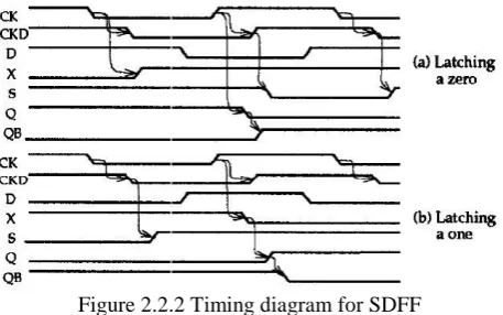
A block diagram of a semi-dynamic flip-flop (SDFF) is shown in Fig. 3.2.1 The circuit is composed of a dynamic front-end and a static backfront-end. The flop samples input D and produces output QB, which is the logic complement of D. The circuit operates as follows. On the falling edge of clock CK, the flop enters the pre charge phase. Node X is pre charged high, cutting off node Q from the input stage. The static latch INV5-6 holds the previous logic level of Q and QB. Since CKD is also low during pre charge, node S remains high holding transistor N 1 on. The evaluation phase begins with the rising edge of clock CK.
If input D is low (i.e., the flop is latching a zero) node X would remain high, held by the INV3-4 latch. Node Q would either remain low or will be discharged through transistors N4-5, driving QB high (See Fig. 3.2.2(a)).
Figure 2.2.2 Timing diagram for SDFF
Three gate delays after CK rises, node S will be driven low, turning transistor
N1 off. This
shut-off operation will prevent a subsequent low-to-high transition of D from discharging node X. This feature provides the flip-flop its edge-triggered nature. If input D were high prior to evaluation (i.e., the flop is latching a one), node X would be discharged through the pull down path N1-3.The static latch INV3-4 would hold the value of X even if input D were subsequently driven low. The high-to-low transition of X will turn transistor P2 on, driving Q high and output QB low (See Fig. 3.2.2(b)). The falling transition of X would also force node S to remain high, preventing the shut-off of transistor N1, which is unnecessary after node X has been discharged.
Conditional Shutoff
Notice that by using a NAND gate coupled to node X and CKD, the shutoff of the pull down path is conditioned to the state of input D. If D is high prior to evaluation, signal CKD is blocked and no shutoff is performed. This feature allows reducing the sampling window by about one inverter delay, which means a shorter hold time for the flip-flop and a better input noise rejection.
One important advantage of SDFF is that scan circuitry can be added to the basic design with nearly zero hit in performance, in contrast to the flip-flop reported in yet. Another main advantage is that logic functions can be easily incorporated in its dynamic front-end. In fact, most logic functions available in Domino logic can also be built into this flop, such as wide OR functions, multiplexors, and complex gates.
Although SDFF is capable of offering efficiency in terms of speed and area, it is not a good solution as far as power consumption is concerned. Not too many attempts have been made to design a flip-flop, which can incorporate logic efficiently in terms of power, speed and area
2.3
HYBRID LATCH FLIP-FLOP (HLFF)Hybrid Latch Flip-Flop is one of today’s high performance flops. It introduces new mechanism of performing flip-flop functionality based on generating explicit transparency window where the transition is allowed. This approach greatly reduces the complexity of the locking mechanism, resulting in small area and small delay. Moreover, explicit presence of the transparency window allows the use of simpler latch structure in the second stage and gives the circuit robustness to the uncertainty of the clock arrival, known as soft-clock edge property. However, use of this design is associated with considerable power consumption
.
C
ircuit is shown in Figure 3.3. Transparency window is defined by the Propagation time of three inverters. The first stage of the circuit conditionally generates the glitch in the transparency window based on the level of input (D) signal. It can be easily noticed that it is formed by static 3-input CMOS NAND gate, which has the functionality for wanted glitch generation. Second stage captures the generated glitch. If the glitch has not appeared (corresponds to low level of input), the output is brought to zero.Figure 2.3 Hybrid latch flip-flop (HLFF)
Also, the circuit suffers from an unwanted glitch at the output, generated by the race condition. This happens because the second stage assumes the default state of internal node (X) to be high (no glitch at the node X is a signal for resetting the output). If the previous flip-flop state was high and under realistic assumption of non-zero propagation time from the active clock edge to the transition of the internal node, it is easily seen that the output will make falsetransition from high to low level, returning again to high level after the transition of internal node. Chosen technique for keeping the output at the defined state (avoiding dynamic behavior) also has certain shortcomings. The keeper is used to hold the value of a dynamic node that would otherwise be in high impedance and therefore sensitive to leakage current effects and noise, especially in low-
power
applications where clock gating techniques are usually employed.This simple method has some disadvantages as well: in order to change the state of HLFF, the keeper has to be overpowered, which introduces another portion of unnecessary power consumption and increase in the delay. This is particularl y true for the keeper at the output since in some cases, such as pass-transistor logic driven by flip-flop, it has to have certain minimal driving capability, which is the requirement in conflict with the claimed keeper weakness. These disadvantages make HLFF not suitable for applications where low power is required since its power consumption limits its utilization. It is noticed that considerable portion of power dissipated in HLFF occurs due to these unnecessary and false transitions that result in glitches generally increasing the power consumed by consecutive logic as well.
2.4
CONDITIONAL DATA MAPPING FLIP-FLOP
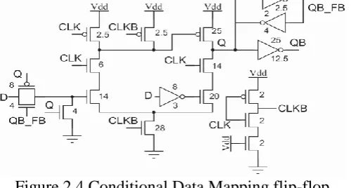
Conditional data mapping flip-flop (CDMFF) is purely dynamic- most efficient structure. In CDMFF unwanted transitions are eliminated by using an output feedback structure to conditionally feed the data to flip-flop. Thus when a redundant event is predicted this architecture reduces power dissipation by eliminating unwanted transitions.
The conditional data mapping flip-flop use only seven clocked transistors, resulting in about 50% reduction in the number of clocked transistors, hence CDMFF used less power than other flip-flop designs. This shows the effectiveness of reducing clocked transistor numbers to achieve low power. However, there is redundant clocking capacitance in CDMFF.
Fig. 3.4 shows the Architecture of CDMFF. When data remains 0 or 1, the pre charging transistors, P1 and P2, keep switching without useful computation, resulting in redundant clocking. Clearly, it is necessary to reduce redundant power consumption here. Further, CDMFF has a floating node on critical path because its first stage is dynamic. When clock signal CLK transits from 0 to1, CLKDB will stay 1 for a short while which produces an implicit pulse window for evaluation. During that window, both P1, P2 are off. In addition, if D transits from 0 to 1, the pull down network will be disconnected by N3 using data mapping scheme (N6 turns off N3); If D is 0, the pull down network is disconnected from GND too.
Hence internal node X is not connected with Vdd or GND during most pulse windows, it is essentially floating periodically. With feature size shrinking, dynamic node is more prone to noise interruption because of the undriven dynamic node. If a nearby noise discharges the node X, pMOS transistor P3 will be partially on, and a glitch will appear on output node Q
Figure 2.4 Conditional Data Mapping flip-flop
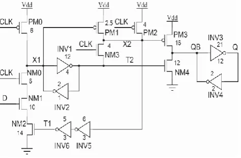
2.5 CROSS CHARGE CONTROL FLIP-FLOP (XCFF)
Several hybrid flip-flop designs have been proposed in the past decade, to reduce power, delay, and area. Recent flip-flop architecture named Cross Charge Control Flip Flop (XCFF) has some advantages over SDFF and HLFF in both power and speed. It reduces the pre-charge capacitance by means of using split-dynamic node, which causes the large power consumption in most of the existing designs.
Figure 2.5 Cross Charge Control flip-flop (XCFF)
Cross charge control flip-flop has large pre charge capacitance in a wide variety of designs results from the fact that both the output pull-up and the pull-down transistor are driven by this pre charge node. These transistors being driving large output loads contribute to most of the capacitance at this node. This common drawback of many conventional designs was considered in the design of XCFF. It reduces the power In addition to the large hold time requirement resulting from the conditional shutoff mechanism a low to high transition in the CLK when the data is held low can cause charge sharing at node X1. (See Fig 3.5) This can trigger erroneous transition at the output unless the inverter pair INV1-2 is carefully skewed. This effect of charge sharing becomes uncontrollably large when complex functions are embedded into the design. X2 is purely dynamic. An unconditional shutoffmechanism is provided at the frontend instead of the conditional one in XCFF.
XCFF diminishes the power dissipation by splitting the dynamic node into two, every one independently driving the output pull-up and pull-down transistors. Since stand out of the two dynamic nodes is exchanged amid one CLK cycle, the total power utilization is impressively lessened without any degradation in speed. Likewise XCFF has a nearly lower CLK driving load. One of the significant downsides of this configuration is the redundant pre charge at node X2 and X1 for information examples holding more 0 s and 1 s, separately. In addition to the vast hold time prerequisite coming about because of the conditional shutoff mechanism, a low to high move in the CLK when the information is held low can result in charge sharing at node X1. This can trigger mistaken move at the output unless theinverter pair Inv1-2 is precisely skewed. This impact of charge sharing gets to be wildly vast when complex capacities are inserted into the design
.
III. PROPOSED ARCHITECTURE
3.1DUAL EDGE-TRIGGERED FLIP-FLOPS
Clock related power is one of the most significant components of the dynamic power consumption. The total clock related power dissipation in synchronous VLSI circuits is further divided into three major components: power dissipation in the clock network, power dissipation in the clock bowers, and power dissipation in the Flip-Flops. The total power dissipation of the clock network depends on both the clock frequency and the data rate, and can be computed based on Equation
PCK = Vdd2[fCK(CCK + Cff;CK) + fDCff;D]
Where CLK is the clock frequency; D is the average data rate; CCK is the total capacitance seen by the clock network; Cff;CLK is the capacitance of the clock path seen by the Flip-Flop; Cff;D is the capacitance of the data path seen by the Flip-Flop.
expression. By reducing the overall capacitance of the clock network, CCK, the power dissipation may also be reduced. For instance, the capacitance can be reduced by proper design of clock drivers and bowers.
Similarly, by reducing the capacitance inside a Flip-Flop, Cff;CK and Cff;D, power may also be reduced. Furthermore, the clock power dissipation is linearly proportional to the clock frequency. Although the clock frequency is determined by the system special applications, it can be reduced with the use of dual edge triggered Flip-Flops (DETFFs). As its name implied, DETFF responds to both rising and falling clock edges. Hence, it can reduce the clock frequency by half while keeping the same data throughput. As a result, power consumption of the clock distribution network is reduced, making DETFFs desirable for low power applications.
Even for high performance applications, the usage of DETFFs. Since the clock speed is reduced by a factor of two, one does not need to propagate a relatively high speed clock signal. A classic double-edge triggered Flip-Flop can be implemented as in Figure 12. In this classic configuration, two opposite polarity level-sensitive latches are connected in parallel; the output is then multiplexed at the output stage.
The Flip-Flop, DETgago, proposed in is illustrated in Figure. Nodes N2, N3, N4, and N5 represent parallel connections between input buyers and latches. The appropriate phase of clock and its complement connects and disconnects the input bowers and storage elements from the power supply and ground. When CK is high, the top input buyers and the bottom latch are active while the bottom input buyers and the top latch are inactive, and vice versa. As a result, it has potential for low power applications.
Although the complete isolation of the active and inactive parts of the circuit helps in power savings, it leads to a larger delay.
The circuit implementation of DET Flip-Flops proposed in [4] which is a modified version of the DETFF proposed. Complementary transmission and logic gates are employed here to balance the output rise and fall times of the original DETFF. With this modification, it improves the power and the latency at the expense of increased total transistor count
The proposed a DETFF. In this DETFF, the role of the clock enable signal and the input data signal is reversed in the feedback transmission gate loops of the storage latches. This implementation can reduce the number of transistor count at the expense of increased latency. Consider an operation at a falling clock edge.
Figure 3.1 Dual edge-triggered flip-flops
transmission gates are closed, M6 now passes a 1 (CK) onto N1, further enhances the value stored. A similar approach can be used to study the case for D equal 0.
IV. IMPLEMENTATION AND ANALYSIS
The proposed DETFF, DET proposed, is illustrated in Figure 3.6. It consists of two sets of back-to-back inverters as storage elements. A true and complement combination of input data and clock signals controls the latching of the data value in these storage elements. When CK is high, node N7 is pre-discharged to 0. If D is 1, then N1 is pulled down to 0. Else if D is 0, then N2 is 0 and N1 becomes a 1.
The main advantage of this configuration is that it avoids stacking PMOS transistors. As a consequence, low voltage and low power operation becomes feasible.
In the proposed design, the transmission gate based DETFF (T_DETFF) in the existing design has been replaced by another modified DETFF. Since, DETFF’s are edge sensitive devices; data can be latched on anyone of the clock edges. Though several contributions have been made to design DETFF’s, there arises certain circumstance to reduce the Power consumption of DETFF’s further. A high performance DETFF proposed shown in Fig 3 consumes less power and area than the other designs and will be more suitable for high performance applications.
TypeofFlip-Flop No.of
Transistors
Average Power (Watts)
Delay(Seconds)
PC 603 28 1.662 3.85
SDFF 22 1.607 3.48
HLFF 53 3.680 9.34
CDMFFME1 40 6.771 3.95
XCFF 31 4.180 5.54
PROPOSED 1SCHEME1 30 5.980 2.12
Fig 4.1Analysis and Timing diagram of DETFF
Figure 4.2 Power analysis and delay diagram of DETFF
Conclusion
Due to high demand of power efficient mobile devices, various power reduction techniques have been emerged. When used separately, the DETFFs has proved to be very efficient flip-flop design in reducing power but when used or integrated with clock gating technique data miss-communication errors occurs due to asynchronous data sampling. In order to eradicate this problem several solutions have been suggested and two simple approaches were introduced to reduce the power consumed in DETFF’s by eliminating the asynchronous data sampling issue. In order to reduce the power consumption further, a new design has been proposed and based on that, two designs were implemented using Tanner EDA tool.
FUTURE WORK
Reference Papers:
[1] K. Absel, L. Manuel, and R. K. Kavitha, “Low-Power Dual Dynamic Node Pulsed Hybrid Flip-Flop Featuring Efficient Embedded Logic”, in IEEE Transactions on VLSI systems, Vol. 21, no. 9, September 2013,pp. 1693-1704
[2] K. Ramesh, K. S. Kumar and S. Jagadeesh, “Analysis of Dual Dynamic node Flip-Flop with Embedded Logic module on Tanner”, in IJARECE Volume 3, Issue 9, September 2014,pp.1186-1192
[3] M. Pelleti, T. K. Murthy and K. Neelima3, “ Low-Power and Low-Area Dual Dynamic Node Hybrid Flip-Flop Featuring Efficient Embedded Logic for Low Power CMOS VLSI Circuits Using 120nm Technology”, in IJETAE Volume 4, Issue 8, August 2014, pp. 471-476
[4] K. Jindal, Renu and V.K.Pandey, “Design of Conditional Data Mapping Flip-Flop for Low Power Applications”, in (IJISME) ISSN: 2319-6386, Volume-1, Issue-5, April 2013,pp.72-75
[5] N. Nedovic and V. G. Oklobdzija, “Hybrid latch flip-flop with improved power efficiency,” in Proc. Symp. Integr. Circuits Syst. Design, 2000, pp. 211–215.
[6] F. Klass, “Semi-dynamic and dynamic flip-flops with embedded logic,” in Proc. Symp. VLSI Circuits Dig. Tech. Papers, Honolulu, HI, Jun. 1998, pp. 108–109.
[7] M. Keating, D. Flynn, R. Aitken, A. Gibbons, and K. Shi, Low Power Methodology Manual: For System-on-Chip Design. New York:Springer, 2007.
[8] M. Pedram, “Power minimization in IC design: Principles and applications,” ACM Trans. Design Autom. Electron. Syst. (TODAES), vol. 1, no. 1, pp. 3–56, 1996.
[9] V. Venkatachalam and M. Franz, “Power reduction techniques for microprocessor systems,” ACM Comput. Surveys (CSUR), vol. 37, no. 3, pp. 195–237, 2005.
[10] C.-C. Yu, “Low-power double edge-triggered flip-flop circuit design,” in Proc. Int. Conf. Innovative Computing Information and Control(ICICIC), 2008, p. 566.
[11] A. G.M. Strollo, C. Cimino, and E. Napoli, “Power dissipation in onelatch and two-latch double edge triggered flip-flops,” in Proc. IEEE Int.Conf. Electronics, Circuits and Systems, 1999, vol. 3, pp. 1419–1422.
[12] R. Hossain, L. Wronski, and A. Albicki, “Low power design using double edge triggered flip-flops,” IEEE Trans. Very Large Scale Integr.(VLSI) Syst., vol. 2, no. 2, pp. 261–265, 1994.
[13] A. G. M. Strollo, E. Napoli, and C. Cimino, “Analysis of power dissipation in double edge-triggered flip-flops,” IEEE Trans. Very LargeScale Integr. (VLSI) Syst., vol. 8, no. 5, pp. 624–629, Oct. 2000.
[14] N. Nedovic and V. G. Oklobdzija, “Dual-edge triggered storage elements and clocking strategy for low-power systems,”
IEEE Trans. VeryLarge Scale Integr. (VLSI) Syst., vol. 13, no. 5, pp. 577–590, Oct. 2005.
[15] V. Stojanovic and V. G. Oklobdzija, “Comparative analysis of masterslave latches and flip-flops for high-performance and low-power systems,” IEEE J. Solid-State Circuits, vol. 34, no. 4, pp. 536–548, Apr. 1999.