Design and Implementation of AMBA AXI 4.0 Master for
High-Speed Performance SoC
SYEDA NASIHA1, VEERESH PUJARI 2 and Dr. Baswaraj Gadgay3
1
Dept. of VLSI Design & Embedded Systems, PG Student, VTU PG Centre, Kalaburagi-585104, INDIA,
2
Dept. of VLSI Design & Embedded Systems, Assistant Professor, VTU PG Centre, Kalaburagi-585105, INDIA,
3
Dept. of VLSI Design & Embedded Systems, Research Guide and Professor, VTU PG Centre, Kalaburagi-585105, INDIA,
Abstract
Advanced microcontroller bus architecture (AMBA) protocol family provides solution to replace complex bridges with specific protocols for components interconnect on SoC designs. It enables comprehensive testing of interface IPs in simpler manner and removing cost and time effort to companies. The proposed AMBA AXI 4.0 provides burst lengths up to 32 beats, with updated write response requirements, removed locked transactions and includes information on the interoperability of components. This protocol supports 16 masters and 16 slaves interfacing. And this paper presents work on design and implementation of AMBA AXI4 Master Model for high performance SoCs using Verilog HDL coding and simulation results are shown using Xilinx tool.
Keywords: VLSI-Very Large Scale Integration, ADVANCED MICROCONTROLLER BUS ARCHIRECTURE (AMBA), ADVANCED EXTENSIBLE BUS (AXI), MASTER INTERFACE.
1. INTRODUCTION
The AMBA Advanced Extensible Interface bus, generally called AXI protocol and it is proposed mainly to overcome the limitations over the AHB, for high-frequency memory or peripheral transactions requirement in an SOC. This specification provides faster and flexible interconnect network between the master and slave devices in SOC. AXI has multiple of features than AHB. Some of the key features of the AXI protocol are separate address/control and data phases, support for unaligned data transfers using byte strobes, burst-based transactions with only start address issued, separate read and write data channels to enable low-cost Direct Memory Access.
And this protocol permits address information to be issued ahead of the actual data transfer, as well as supports multiple outstanding transactions and
out-of-order completion of transactions. ARM has released with different versions of AMBA AXI protocol as per requirement. Currently AXI 4.0 protocol is using for high performance system on chip designs with multiple features and applications like Smart Phones, Tablets and high speed computers SOC.
2. LITERATURE SURVEY
Shrinking process technologies and increasing design sizes have led to highly complex billion-transistor integrated circuits (ICs). As a consequence, manufacturers are integrating increasing numbers of components on a chip. A heterogeneous system-on-a-chip (SoC) might include one or more programmable components such as general purpose processors cores, digital signal processor cores, or application specific intellectual property (IP) cores, as well as an analog front end, on-chip memory, I/O devices, and other application specific circuits.
www.ijiset.com
bus protocol has become the de facto standard SoC bus. That means more and more existing IPs must be able to communicate with AMBA4.0 bus. AMBA bus architecture is an SoC communication protocol that aims at high performance and low power consumption by partitioning based on the bandwidth with which the devices operate, within the system.
The first AMBA buses were Advanced System Bus (ASB) and Advanced Peripheral Bus (APB). In its second version, AMBA 2, ARM added AMBA High-performance Bus (AHB) that is a single clock-edge protocol. In 2003, ARM introduced the third generation, AMBA 3, including AXI to reach even higher performance interconnects and the Advanced Trace Bus (ATB) as part of the Core Sight on-chip debug and trace solution. In 2010 the AMBA 4 specifications were introduced starting with AMBA 4 AXI4, then in 2011 extending system wide coherency with AMBA 4 ACE with a re-designed high-speed transport layer and features designed to reduce congestion [5-7].
Fig. 1 Different versions of AMBA
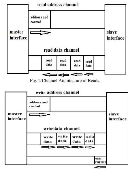
3. EXISTING AXI PROTOCOL ARCHITECTURE
• Write Channel: Write address, data and
Write Response signals.
The data transactions happen in either of the two ways:
• A write data channel to transfer data from
the master to the slave. In a write transaction, the slave uses the write response channel to signal the completion of the transfer to the master.
• A read data channel to transfer data from the slave to the master.
Fig. 2 Channel Architecture of Reads.
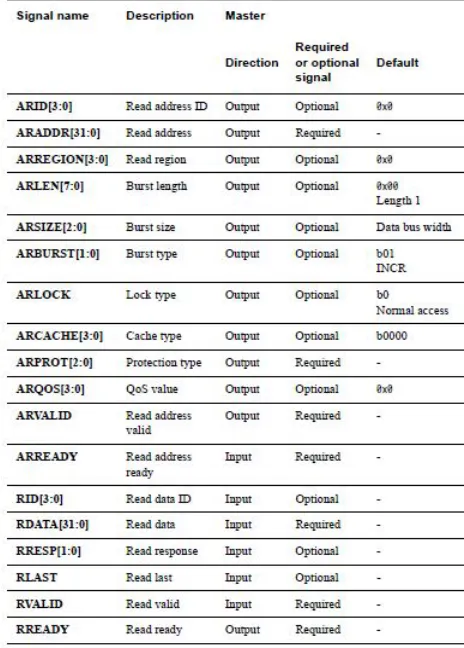
4. PROPOSED AXI MASTER ARCHITECTURE AND SIGNALS
An AXI 4.0 Master design for memory or peripheral device to achieve communication between processor and with device.
There are five channels and designed with five state machines. State machines for write address, write data and write response, as well for read address and read data. Using following signals.
For above master transactions happens using handshake mechanism and signals called READY/VALID. Flexible design for multiple data or burst transactions between master and slave are proposed.
Fig. 5 Internal architecture of AXI4.
Table 1: Master Write Channel interface signals.
Table 2: Master Read Channel Interface Signals
5. HARDWARE IMPLEMENTATION
Data is transferred from the AXI_4 master to seven segment at variable speeds of 25Mb/s, 50Mb/s and 100Mb/s as shown in figures below.
www.ijiset.com
Fig. 7: Data Transfer at 100Mb/s.
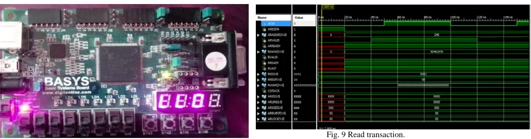
6. REQUIRED SIMULATION RESULTS
An AXI_4 master interface is designed and executed to build up correspondence between modules of SoCs like CPU, DMA, RAM, and different peripherals at a high transfer speed of 1GHz.
The write operation is initiated when control data and address is sent on the address channel defined for write operation by a master_device. The data to be written in to the slave device is then sent on the data channel specified for write operation by master. The valid indication is kept low up to the time when write information becomes accessible. At the end last data item WLAST is sent by the source device indicating the completion of transaction.
In response to the WLAST signal sent by source device, the destination device drives a write response signal BRESP [1:0] high after when it has acknowledged the entire information sent by source device. This response signal demonstrate the completion of write transaction. The permissible responses are DECERR, OKAY, SLVERR and EXOKAY. Similarly the read operation takes place when the address to be read becomes available on the address channel. Read data channel is used to exchange corresponding information as appeared in figure 9.
Fig. 9 Read transaction.
VALID sign is kept low by the slave_device up to the time when information to be read becomes accessible. Destination affirms the RLAST signal, after the information exchange of burst is completed in order to demonstrate that the final data for the particular transaction has been exchanged successfully. The signal RRESP [1:0] demonstrates the condition of read exchange. 16 outstanding transactions are underpinned by this convention, so that every read/write exchanges have ARID [3:0] AWID [3:0] respectively.
7. CONCLUSION AND FUTURE SCOPE
Finally, the requirements of bus are defined and also design approach for implementation and testing of module are specified. This bus supports high frequency data transactions between master and slave depending on technology used for SOC and also based on application. Write and Read operations happens from master to slave on requirement for 100MHz on Xilinx FPGA.
Following the latest AXI specifications, the designed bus can easily be used to connect different peripherals like SPI, I2C, UART etc., into non AMBA based processors.
In spite of its name, the extent of advanced microcontroller bus architecture has gone considerably exceeding the micro controller devices. ASIC and SoC parts like application processors of mobile devices like smart phones uses this bus architecture. Current proposal is only implemented till the AXI4 protocol. It can be further enhanced to implement for AXI4ACE so that it can be used in almost each of the developing SoC targeted for the mobile phones and the tablet market.
[3] Design of AMBA AXI4 protocol for System-on-Chip communication, International Journal of Communication Network and Security (IJCNS), Vol-1, Issue-3 ISSN: 2231-1882.
[4] Design and Implementation of AMBA based AXI 4 Slave Interface, IJIRSET, Vol. 4, Issue 6, June 2015.
[5]”AMBA AXI 4 and ACE Protocol Specification” 28 October 2011 D Non-Confidential First release of AMBA AXI 4 and ACE Protocol Specification.
[6] Xu Yang ; Harbin Inst. of Technol., Harbin ; Zhang Qing-li ; Fu Fang-fa ; Yu Ming-yan, “NISAR: An AXI compliant on-chip NI architecture offering transaction reordering processing” ASIC, 2007. ASICON '07. 7th International Conference, 22-25 Oct. 2007.
[7] Manjula, R.B. ; Manvi, S.S. ; Kaunds, P. “Data transactions on system-on-chip bus using AXI4 protocol” Recent Advancements in Electrical, Electronics and Control Engineering (ICONRAEeCE), 2011 International Conference, 15-17 Dec. 2011.
[8] “Verilog-A Language Reference Manual Analog Extensions to Verilog HDL”, Version 1.0, Open Verilog International August 1, 1996
[9] “Verilog-AMS Language Reference Manual”, Release 2.3.1, Accellera Systems Initiative , 06-2009