VICTORIA :
UNIVERSITY
r% x z o
r-o
a -<
THE DESIGN OF AN H^ VOLTAGE REGULATOR
FOR A PREDICTIVE CURRENT CONTROLLED
THREE PHASE P W M P O W E R CONVERTER
A Thesis Submitted for Examination for the Degree of Master of Engineering
in Electrical and Electronic Engineering
By MING YU
B.E. Shanghai Jiao Tong University Shanghai P R C
A n investigation carried out within
School of Communications and Informatics
Faculty of Engineering and Science
V I C T O R I A U N I V E R S I T Y O F T E C H N O L O G Y
Footscray Victoria Australia
PTS THESIS
621.317 YU
3
oooio
05559242 yI
DECLARATION
This thesis contains no material which has been accepted for the award of any other degree or diploma in any university or other institution. T o the best of m y knowledge the material is original and has not been previously written or published by any other person, except where due reference is m a d e in the text of the thesis.
ABSTRACT
In this project, an Hm controller is proposed as a D C voltage regulator for the predictive
current controlled pulse width modulated ( P W M ) three-phase power converter to compensate the uncertainty caused by the predictive current controller. T h e Hm theory
has its unique approach to the uncertainty issue, its design method allows both the stability robustness and performance robustness to be considered at the design stage.
The design of the HM voltage regulator is based on the worst case scenario where the
converter is subject to a load disturbance and its operation m o d e is changed from the rectifying to the regeneration, consequently, parameters and structure of the original plant transfer function derived, vary significantly. T h e proposed Hx ( D C ) voltage regulator is
to overcome the uncertainty problem and to w o r k with the predictive current controller to achieve robust control of the entire system.
The combined control scheme is simulated using MatLab/SIMULINK environment. The simulation results s h o w that the closed-loop system is capable of achieving performance robustness and stability robustness for the worst case scenario. T h e output D C link voltage is stable and nearly sinusoidal, while the line currents are delivered with a unity power factor.
iii bed for conducting experimental research in the area of converter control and machine
control.
To summarize the work accomplished by the author for this project:
1. The introduction of the Hm control theory into the application of converter control and
theoretical design of the Hm voltage regulator;
2. The simulation of the entire closed-loop controlled power converter with the combination of a predictive current control and a Hn voltage regulator;
ACKNOWLEDGMENTS
I would particularly like to acknowledge the invaluable guidance and considerable assistance of m y principal supervisor, Dr. Qin Jiang throughout this project. Dr. Jiang gives m e her enthusiasm for basic research and willingness to discuss and challenge ideas at any time. I can not imagine a better supervisor.
Special thanks are also extended to my co-suoerisor, Dr. Li Ge Xia for his help in the final stages of completing m y thesis.
During my research I have benefited from discussions with Dr. Ying Tan and Mr Michael Wingate. I wish to express here m y sincere thanks to Dr. Tan and M r Wingate for their assistance throughout this project.
Finally, but not least, I am greatly indebted to my wife for her understanding and caring throughout these years. Without her support, encouragement and patience, this thesis
V
CONTENTS
C O N T E N T S V
LIST OF TABLES rx
LIST OF ILLUSTRATIONS X
Chapter 1 Introduction 1
1.1 Introduction 1
1.2 Review of the Modulator Scheme 2
1.2.1 Delta Current Regulator 2 1.2.2 Hysteresis Current Controller 3 1.2.3 Stationary Frame R a m p Comparison Regulator 4
1.2.4 Natural Sampled P W M 4 1.2.5 Regular Sampled P W M 5 1.2.6 Space Vector P W M 6 1.2.7 Overmodulation 8 1.3 Review of the Control Scheme 9
1.3.1 Hysteresis Current Control Strategy 9 1.3.2 Current Control Converter in Stationary
and Rotating Frames 10 1.3.2.1 Stationary Frame Controller 11
1.3.2.2 Rotating Frame Controller 11 1.3.3 Predicted Current Control with a Fixed
Switching Frequency (PCFF) 12 1.4 S u m m a r y of Literature Review 13
2.1 Introduction 16 2.2 The Model of the P W M A C / D C Converter 16
2.3 P C F F Control System 18 2.3.1 P C F F Control L a w 1Q 2.3.2 P C F F Control System in Rotating Frame of Reference 21
2.4 The Model of P C F F Control System 23
2.4.1 D C Model 23 2.4.2 A C Model 25 2.4.3 Transfer Function Between Peak Line Current
and Control Signal 27
2.5 Summary 30
Chapter 3 The Design of the HK Controller 31
3.1 Introduction 31 3.2 The Preliminary of H ^ Control Theory 32
3.2.1 Singular Values 32
3.2.2 Spaces, H2 and !!,„Norms 33
3.2.3 Standard Representation for HB Problem 34
3.2.4 The HM Problem Formulation 35
3.3 Design of the H M Controller 3 8
3.3.1 A 1 O k V A Model Power Converter 3 8
3.3.2 Design of the H ^ Voltage Regulator 40
3.4 The Performance of the H M Control System 46
3.4.1 The Absolute Stability of the System 46 3.4.2 The Relative Stability of the System 47 3.4.3 Stability Analysis in the z Plane 49
3.5 Summary 51
Chapter 4 Simulation and Simulation Results 52
4.1 Introduction 52 4.2 The Simulation Package Used 53
Vll
4.3.1 The P C F F Controller Subblock 56 4.3.2 The P W M Modulator Subblock 57 4.3.3 The Crossover Delay Subblock 58
4.3.4 The HM Controller Subblock 60
4.3.5 The Phase Lead Subblock 60 4.3.6 The Step Signal Generator Subblock 61
4.4 Step Response of the System 62 4.4.1 Rectifying Operation 62 4.4.2 Regeneration Operation 64
4.5 Dynamic Performance 66 4.5.1 Transient Response D u e to a Step Change in
the D C Voltage Reference 66 4.5.2 Transient from the Rectifying to the Regeneration 67
4.6 Summary 69
Chapter 5 Development of Experimental System 70
5.1 Introduction 70 5.2 Voltage Source Converter 71
5.2.1 The Operation of A C / D C Converters 71
5.2.2 Gate Driver Circuit 73 5.3 The Single Chip PC-486 Controller 75
5.4 The P W M Generator Board 79 5.4.1 Control Block 79 5.4.2 Timer Board 81 5.4.3 Synchronizing Unit 83
5.4.4 Crossover Delay Circuit 84 5.5 Software Development of Control of P W M Board 85
5.6 Data Acquisition and Conversion Board 88 5.6.1 The Analog-to-Digital Conversion B oard 88
5.6.2 Current and Voltage Transducers 89
6.1 Introduction 92 6.2 The Design of Power Filter 92
6.3 Experimental Results 94 6.3.1 Experimental Results of Synchronizing Unit 94
6.3.2 Experimental Results of P W M Generator Board 94 6.3.3 Experimental Results of the Crossover Delay Circuit 96 6.3.4 Experimental Results of the Voltage Source Converter 98
6.4 Summary 104
Chapter 7 Conclusions and Further Work 105
7.1 Conclusions 105 7.2 Further W o r k 106
7.2.1 Further Theoretical work 106 7.2.2 Further Practical W o r k 107
References 108
Appendix A Circuit Schematics 111
A l I G B T Driver 112 A 2 P W M Generator Board 113
Appendix B Software Programs 114
B 1 Simulation Function 114 B 2 Computer Program 117
IX
LIST OF TABLES
Table 5.1 Space Vector P W M Algorithm 78
Table 6.1 The Experimental Results of the Converter 98
LIST OF ILLUSTRATIONS
Figure 1.1 Per Phase Delta Current Regulator Structure Figure 1.2 Hysteresis Current Regulator
Figure 1.3 Phase SFRC Current Regulator Structure Figure 1.4 Natural Sampled P W M
Figure 1.5 Regular Sampled P W M
Figure 1.6 Switch Configuration and Target Phase from Space Vector Figure 1.7 Space Vector P W M Waveform in One Switching Period Figure 1.8 Hysteresis Current Control
Figure 1.9 Current Control in Stationary Frame Figure 1.10 Current Control in Rotating Frame
Figure 1.11 Block Diagram of the PCFF Control System Figure 2.1 The Circuit of P W M AC/DC Converter Figure 2.2 Block Diagram of the PCFF Control System Figure 2.3 The Waveform of Voltage Trigger Converter Figure 3.1 Standard Configuration
Figure 3.2 Multiplicative Unstructured Uncertainty Figure 3.3 The Bode Plot of Design Principles Figure 3.4 The H„ Controlled PCFF Converter
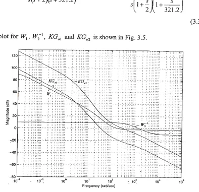
Figure 3.5 Bode Plot of Wx, W2~ l
, KGol and KGo2
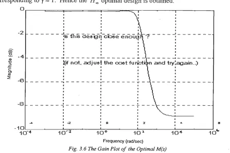
Figure 3.6 The Gain Plot of the Optimal M(s)
Figure 3.7 Determination of Gain Margin and Phase Margin on the Bode Plot of LO1 (s)
Figure 3.8 Determination of Gain Margin and Phase Margin on the Bode Plot of Lo2 (s)
Figure 3.9 The Discrete-Time PCFF Control System with Hm Controller
Figure 4.1 Three Phase P W M AC/DC Converter
Figure 4.2 Simulation Block Diagram of Three Phase Predictive P W M AC/DC Converter with Hm Controller
3 3 4 5 6 7 8 10 11 12 12 17 19 20 34 36 37 39
44 45
48
48 49 52
XI
Figure 4.3 The Configuration of the P C F F Controller Subroutine 57 Figure 4.4 The Configuration of the P W M Modulator Subroutine 58 Figure 4.5 The Simulation Structure of Crossover Delay Subroutine 58
Figure 4.6 The Simulation Results of Gating Signals 59
Figure 4.7 The Configuration of the Ha Controller Subroutine 60
Figure 4.8 The Configuration of Phase Lead Subroutine 60 Figure 4.9 The Configuration of the Step Signal Generator Subroutine 61
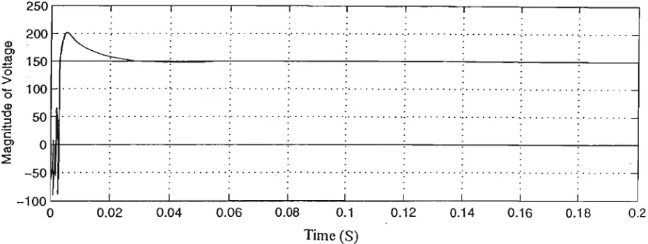
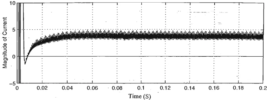
Figure 4.10 Step Response of D C Output Voltage in the Rectifying M o d e 62 Figure 4.11 Step Response of D C Output Current in the Rectifying M o d e 63 Figure 4.12 Step Response of Line Current and Line-to-Neutral Voltage
in the Rectifying M o d e 63 Figure 4.13 Sample-Hold Modulating Waveform and
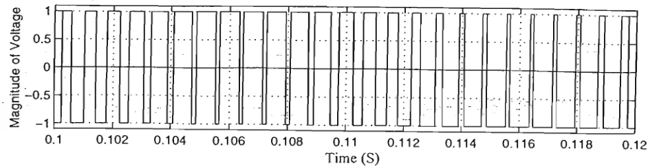
Carrier Waveform in the Rectifying M o d e 63 Figure 4.14 Steady-State Pulse Width Modulated Waveform
in the Rectifying M o d e 64 Figure 4.15 Step Response of D C Output in the Regenerating M o d e 65
Figure 4.16 Step Response of D C Output Current in the Regenerating M o d e 65 Figure 4.17 Step Response of Line Current and Line-to-Neutral Voltage
In the Regenerating M o d e 65 Figure 4.18 Transient Performance of D C Output Voltage in the Input Change 66
Figure 4.19 Transient Performance of D C Output Current in the Input Change 67 Figure 4.20 Transient Performance of Line Current and Line-to-Neutral
Voltage in the Input Change . 67 Figure 4.21 Transient Performance of D C Output Voltage in the Load Change 68
Figure 4.22 Transient Performance of D C Output Current in the Load Change 68 Figure 4.23 Transient Performance of Line Current and Line-to-Neutral 68 Figure 5.1 Circuit Diagram of the Three-Phase Voltage Source Converter 71 Figure 5.2 Three-Phase Leg Voltage Source Converter
with O n e Phase S h o w n Only) 72 (a) Line Current Flows in Positive Direction 72
(b) Line Current Flows in Negative Direction 72 Figure 5.3 The Waveform of Driving Signal and Phase Leg Voltage 73
(c) Phase Leg Voltage Waveform with Line Current
in Negative Direction
Figure 5.4 Block Diagram of I G B T Gate Driver
Figure 5.5 Overload Detection for I G B T Devices
Figure 5.6 PC-486 Controller
Figure 5.7 Pin Configuration of PC-486 Terminal
Figure 5.8 Space Vector P W M Switching Patterns
Figure 5.9 Structure of P W M Generator Board
Figure 5.10 Block Diagram of the Control Block
Figure 5.11 Block Diagram of Timer Board
Figure 5.12 Waveforms of Timer Output and J-K Flip-Flop Outputs
Figure 5.13 Block Diagram of Synchronizing Unit
Figure 5.14 Flow Chart of the Controller Software
Figure 5.15 Flow Chart of the A/D Conversion Software
Figure 5.16 Circuit Connection of Three Current Transducers
And Three Voltage Transducers
Figure 5.17 View of the Computer Controlled Three-Phase
Voltage Source converter
Figure 6.1 The Circuit of Three-Phase P W M A C / D C Converter
Figure 6.2 Experimental Result of Synchronizing Unit
Figure 6.3 Experimental Results of Sampling Signal
and P W M Firing Signal
Figure 6.4 Experimental Results of Utility Phase Voltage
and P W M Firing Signal
Figure 6.5 Experimental Results of Crossover Delay
Figure 6.6 D C Output Voltage of Converter
Figure 6.7 Line Current
Figure 6.8 Experimental Results of D C Link Voltage
and Input Line Current
Figure 6.9 Experimental Results of Line Current
and Line-to-Neutral Voltage
73
74
74
75
76
77
79
81
82
83
84
87
88
89
90
92
94
95
96
97
100
100
101
X1I1
Figure 6.10 Simulation Results of Line Current
and Line-to-Neutral Voltage 102 Figure 6.11 Experimental Results of Line-to-Line Voltage of the Converter 103
Figure 6.12 Simulation Result of Line-to-Line Voltage
at the A C Terminal of the Converter 103
Figure A. 1 IGBT Driver 112
Chapter 1
INTRODUCTION AND LITERATURE REVIEW
Ll INTRODUCTION
Over the last three decades, there have been considerable advances in the design of variable frequency drivers. M o s t power converters on the market today are link type converters in
which an uncontrolled rectifier with a stiff D C voltage supplies an insulated gate bipolar transistor ( I G B T ) or bipolar junction transistor (BJT) inverter bridge. A fairly large capacitor is required in the D C link.
The uncontrolled converter with a large capacitor has a slow dynamic response of DC voltage output and a very poor line current waveform with a large harmonic component which is fed back into the supply network that causes harmonic pollution [1-2]. T h e supply authorities intend to draw u p m o r e restrictive regulations to inhibit such harmonic pollution. In order to satisfy such n e w regulations, the A C drives m a y be redesigned to use controlled converters. O n e approach is to replace the uncontrolled diodes with transistors such as G T O (Gate Turn Off) or I G B T (Insulated Gate Bipolar Transistor). B y controlling the gating signals to these transistors, it is possible to produce sinusoidal current waveforms with a unity power factor at the utility side. This permits a substantial reduction in the size of the D C link capacitor and bidirection power flow between the utility and the load [3-12].
Intensive research work has been carried out in the area of converter control. The work can be divided into t w o major tasks, the design of a controller (or compensator) and a
modulator. Their functions are explained respectively as follows.
(1) The controller is designed based on the specifications such as fast dynamic response of D C voltage, unit power factor and stability of the entire system. T h e control outputs are
CHAPTER 1.
INTRODUCTION A N D LITERATURE REVIEW2
(2) The pulse width modulator generates gating signals to each transistor of the power
converter in terms of the reference inputs from the controller. T h e switching strategy is
selected based o n specifications of harmonic performance of the line current,
electro-magnetic interference ( E M I ) and the efficiency of the converter. For a given switching
strategy, the modulator calculates switching pulses in terms of modulation signal, and
then outputs them to switching devices of the converter. Within the linear modulation
range, the fundamental component of the switching pattern should be proportional to
the sinusoidal modulating waveform.
1.2 REVIEW OF THE MODULATOR SCHEME
It is possible, b y surveying the literature over the last decade, to trace the historical
development of pulse width modulator ( P W M ) techniques and relate these developments to
the changes in technology. T h e delta current regulator, hysteresis current controller, ramp
comparison regulator and natural sampled P W M regulator have been widely used because
of their ease of implementation using analogue techniques. M o r e recently, a switching
strategy referred to as 'Regular' sampling, has been proposed which is considered to have a
number of advantage w h e n implemented using digital or microprocessor techniques. T h e
approach uses the so-called 'Space Vector' and has drawn attention because space vector
modulation is able to lead to a reduced harmonic current ripple compared to other
modulation strategies.
1.2.1 DELTA CURRENT REGULATOR
A m o n g the various well-known current regulated P W M ( C R P W M ) algorithms, the delta
current regulator has an extremely simple and robust structure, and excellent dynamic
performance [3]. T h e switching frequency is bounded by the sampling frequency (Tx).
However, the steady state performance of the regulator is very poor. T h e harmonic content
is large. T h e wide harmonic spectrum includes frequencies from the subsynchronous range
zero states and requires high sampling frequency, hence high average switching frequency as shown in Fig. 1.1. S1 and S2 are drive signals.
Si
(reference current) V ^ _
L
tx>+-
S2i (actual current)
Fig. I. J Per Phase Delta Current Regulator Structure
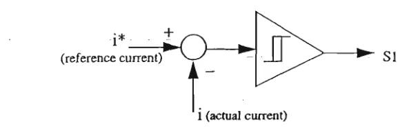
1.2.2 H Y S T E R E S I S C U R R E N T C O N T R O L L E R
The hysteresis current controller is an important P W M technique that is applicable to voltage source converter and inverter [13-14]. A simplified diagram of a typical hysteresis current controller is shown in Fig. 1.2.
(reference current) SI
1 (actual current)
Fig. 1.2 Hysteresis Current Regulator
CHAPTER 1. INTRODUCTION AND LITERATURE REVIEW
1.2.3 S T A T I O N A R Y F R A M E R A M P C O M P A R I S O N R E G U L A T O R
The stationary frame ramp comparison regulator (SFRC) is one of C R P W M strategies [3]
as s h o w n in Fig. 1.3. T h e S F R C has a simple structure and provides well-defined harmonic spectrum. T h e regulator has nonzero steady state error because it operates o n A C signals. If the controller gain Kp is not changed in the proper direction, the phase and magnitude
error of the regulator degrades the performance as the operating point is varied.
(reference) + ;*
I (actual current)
Fig. 1.3 Phase SFRC Current Regulator Structure
1.2.4 N A T U R A L S A M P L E D P W M
Most analogue implemented P W M schemes employ natural sampling technique [5]. It can
0.5
-0.002 0.004 0.006 0.008 0.01 0.012 0.014 0.016 0.018 0.02 P W M Signal
1
0.5
--0.5
-1
0.002 0.004 0.006 0.008 0.01 0.012 O.014 0.016 0.018 0.02
Fig. 1.4 Natural Sampled PWM
1.2.5 R E G U L A R S A M P L E D P W M
CHAPTER 1. INTRODUCTION AND LITERATURE REVIEW
Modulating Signal and Sample Hold Modulating Signal
-0.5
0 0.002 0.004 0.006 0.008 0.01 0.012 0.014 0.016 0.018 0.02 Sample Hold Modulating Signal and Carrier Signal
1
0.5
0
-0.5
-1
1
0.5
0
-0.S
-1rd
0
\ \ l\: •
\ \ / V /
p\"
7i\
h\ i
\ . . « . , —I*/ ~
0 0.002 0.004 0.006 0.008 0 0 1 0.012 0.014 0.016 0.018 0 02 P W M Waveform
0.002 0.004 0.006 0.008 0.01 0.012 Time in Second
0.014 0.016 0.018 0.02
Fig. 1.5 Regular Sampled PWM
1.2.6 SPACE V E C T O R P W M
T h e traditional triangular carrier method has been largely superseded by the 'space vector'
representation m o r e suitable for digital implementation. In this paragraph s o m e basic
features of this method will be reviewed and the relation with the traditional sine triangle
method will be emphasized [4][10-11].
In order to understand space vector PWM, once again look closely at Fig. 1.5 to see what
happens inside one switching period in the case of a single carrier and sinusoidal voltage
reference 120-degree apart. If the signal is high, the top switch of the selected leg is
closed. O n the other hand, if the signal is low, the bottom switch is closed instead. T h e
three phase converter is constituted by six switches and there are eight possible
configurations, as s h o w n in Fig. 1.6 (a). In correspondence of each configuration, the six
switches have a well-defined state: o n or off. A s a consequence, all the possible rectifier
configurations can be identified. W h e n the switch on the top is on, the top bit is 1 and the
bottom bit is 0, and vice versa, for example, switching state S4 in Fig. 1.6 (a) is 011, S5 is
In a three-phase system, the three sinusoidal voltages, 120 degree apart, can be represented by a rotating vector, V , w h o s e projections on the three-phase axis are, instant by instant, the three sinusoidal values.
s4
s6'
s2l
sO
T
1
(1
1
f
|
(
k
\(
[~
( (
k
1
k k
1
k
s5
si
s3
s7
<r
k
(
1
(
k
1
k
j
k
1
k
1
( (
(a) (b)
Fig. 1.6 Switch configuration and Target Phase from Space Vector
T h e voltage reference vector can be synthesized by a combination of three eight states as s h o w n in Fig. 1.6 (b). If the modulating signal frequency is m u c h lower than the switching frequency, then the reference voltage vector can be considered constant during one switching period, Ts. A s a consequence, in a 'time average' sense, the voltage reference
vector in a switching period can be approximated by two active switching states, each for a certain amount of time. In other words, the reference voltage vector is realized, in an average sense, by computing the fraction of the switching period for the two voltage vectors, which are adjacent to V . In Fig. 1.6 (b), /, and t2 are the amount of time spent on
S{ and S2, respectively. Then, in order to keep the switching frequency constant, the
remainder of the switching period is spent on the zero switching state, r0. There is
r0+r,+r2=rt.
CHAPTER 1. INTRODUCTION AND LITERATURE REVIEW
derived for sinusoidal modulation. Refer to Section 5.3 for calculation details of m,, m3
and m5 respectively.
2
V.
~ 2
yM
v
M2
_VL
2
Yi.
2
_vL
2
V -V.
"h
*h
<-ms>
V, V,
-AT
171,-V 171,-V
^ — / A . •
-< m3>.
AT" 2
F/g. /. 7 Space Vector PWM Waveform in One Switching Period
T h e space vector representation is quite useful in digital systems because the microcontroller can calculate the tk, tk+x and Tt and transfer them to a "hardware
modulator'.
1.2.7 OVERMODULATION
1.3 REVIEW OF THE CONTROL SCHEME
U p to n o w , A C / D C conversion has been dominated b y uncontrolled rectifiers or phase
controlled rectifiers. Such rectifiers have the inherent drawbacks that their power factor
decreases w h e n the firing angle increases and that harmonics of the line current are
relatively high. Meanwhile, m o r e and m o r e applications require that the A C / D C converters
have both rectifying and regenerating abilities with fast response to improve the dynamic
performance of the whole system. These, bidirectional power flow and response
requirements have drawn m o r e attention to P W M A C / D C converters. Converters using
hysteresis current control ( H C C ) , current controlled voltage regulated converter in
stationary and rotating frame and predicted current control with fixed switching frequency
( P C F F ) have been very popular. They are capable of delivering nearly sinusoidal current
waveforms with a unity power factor. B y adding D C voltage feedback, they can be m a d e into
stand-along regulated D C voltage supplies with fast response to bidirectional power
demand.
1.3.1 HYSTERESIS CURRENT CONTROL STRATEGY
T h e hysteresis current control ( H C C ) configuration is s h o w n in Fig. 1.8. It looks like an
usual converter including a bridge and a tank capacitor in the D C link [12-14]. O w i n g to
the scheme symmetry, bidirectional power control is possible. T h e bridge, connected to the
supply line ek, is operated so as to absorb sinusoidal currents in phase with the line voltage -.
source. T h e bridge is controlled by a Hysteresis technique in order to obtain accurate
waveform shaping and fast dynamic response. "The tank capacitor stores the amount of
energy needed to keep the D C voltage ripple below a suitable limit, while converter control
keeps constant the D C voltage. T o minimize the tank capacitor, the converter must provide
fast control of the energy exchange between line and storage capacitor. In fact, any input
or output power unbalance causes a variation of the stored energy and, if the capacitor is
small, the D C voltage m a y vary widely.
In order to obtain fast response of the power converter, a hysteresis current control
technique can be adopted, which keeps each current close to its reference, ensuring good
accuracy and small delay time. In any case, s o m e D C voltage variations are unavoidable,
CHAPTER 1. INTRODUCTION A N D LITERATURE REVIEW
In order to keep constant link voltage, Vd, a closed-loop control is introduced. Voltage V
is compared with reference Vdref, and the resulting error signal is fed to a PI regulator,
which provides correcting term. T h e load current is low-pass filtered to obtain average value. A s shown in Fig. 1.8, the current reference amplitude I* is the s u m of the correcting term and load current. In theory, the voltage control loop can work alone. However, sensing the load current ld ensures a feed-forward action, which speeds up the response of
v
d.
The switching frequency of HCC control varies with the DC load current, at heavy loads the frequency increases substantially. T h e switching frequency partem is uneven and random. This presents a major problem for H C C control, in that the instantaneous switching frequency can be even higher than the average switching frequency, causing excessive stress on switching devices.
V V V
To Load
T f T A 4: %_
Current Reference Generator
Hysteresis Current Controller
rjz
L o w Pass Filter
6^
'A refVoltage Regulator
Fig. 1.8 Hysteresis Current Control
1.3.2 C U R R E N T - C O N T R O L L E D C O N V E R T E R IN STATIONARY A N D R O T A T I N G F R A M E S
A current controlled P W M rectifier provides near sinusoidal input currents with a unity
T h e complete rectifier system includes a voltage source P W M converter, a current controller loop and a D C voltage loop as s h o w n in Fig. 1.9. T h e amplitude of the current reference is obtained from the D C voltage loop. The output D C voltage is compared with a voltage reference and the error is fed to a PI (proportional and integral) regulator to reduce the steady state voltage error. T h e output of the PI regulator is then multiplied by input voltage waveforms to provide the three A C current references with the desirable input power factor and proper phase shift. T h e stationary frame controller has the obvious advantage of simplicity since it can be implemented using simple analog circuit. However, the stationary controller regulates A C signals and the integrator has a finite gain at fundamental frequency. Therefore, there is an inherent amplitude and phase error. T h e error depends on the input frequency.
ik
I3Z
P W M Generator
AZ.
Carrier
- •
PI Controller
Load
V,
X PI Controller
< >
+ V d rcf
Fig. 1.9 Current Control in Stationary Frame
1.3.2.2 Rotating F r a m e Controller
T h e rotating frame controller is depicted in Fig. 1.10. T h e three line currents are transferred to (dqo) frame. T h e magnitudes of the reference currents in the rotating frame /, , and / f are dictated by the voltage feedback loop. A n y arbitrarily rotating frame
=h-CHAPTER 1. INTRODUCTION AND LITERATURE REVIEW 12
abc/dq
it
-r-PWM
Generator
HE
dq/abc CarrierTZL
fc
• PI Controller
Load
V,
PIController
PI Controller
o^'
h_Kf=Q Iq_ref
Fig. 1.10 Current Control in Rotating Frame
T h e rotating frame controller eliminates the steady state error, since it operates o n D C
quantities and the integrator has an infinite gain at zero frequency. A lot of digital
calculations are required for the rotating frame controller, so that the implementation is
m o r e complicated. H o w e v e r , for applications which require high accuracy, the rotating
frame controller is the preferred solution.
1.3.3
PREDICTED CURRENT CONTROL WITH A FIXED SWITCHING FREQUENCY(PCFF)
T h e P C F F control system keeps the bidirectional high speed dynamic features but operates
at a fixed switching frequency. It is able to produce nearly sinusoidal line current
waveform with a unity power factor. B y adding a D C voltage feedback, it can be m a d e
into a stand-alone regulated D C voltage supply with fast response to Indirection power
d e m a n d [18-19].
e
k
h
e>*
vik
l k
2£
I
P C F F Controllerl
ck ^ "* 'd_ref
Regulator
C&
Load
reference ick (k = 1,2,3), are produced b y a D C voltage feedback and a load current
feedforward to regulate the D C output voltage Vd. After the regulator, the current
references are modulated by the three-phase source voltage ek with a e je
', where 6 is an
adjustable phase angle for the leading phase shift. T h e angle of the current reference is taken from the angle of the source voltage ek, plus a phase shift 6C, which compensates for
the time delay of the P C F F control. Thus the line current is forced to vary in phase with
ek, and a unity power factor is obtained. T h e use of load feedforward eliminates the
steady-state error that exists w h e n using only proportional D C output voltage feedback. If the proportional plus integral (PI) action is used to control the D C output voltage, the PI regulator can eliminate the steady-state error in the D C output voltage and the load feedforward significantly improves the dynamic response of the D C output voltage due to the load changes.
The detail of the PCFF controlled power converter is shown in the next chapter. In this technique, the modulating voltage Vck required for controlling the line current is calculated
based on the parameters of the power circuit and the switching frequency, this voltage is then compared to a carrier w a v e to generate a switching pattern to regulate the line current. The major shortcoming of the P C F F control is that its control principle is parameter sensitive. T h e power circuit parameters are required to implement the control algorithm. In practice, the difference between a real system model and its mathematical model caused by the variations of these design inputs is the source of system uncertainty and m a y deteriorate the system performance.
1.4 SUMMARY OF LITERATURE REVIEW
CHAPTER 1. INTRODUCTION A N D LITERATURE REVIEW ^ ^ \,
changed from its set point, or when the system is subject to load disturbances [26-27]. The difference between a real system and its mathematical model is a source of uncertainty.
T h e requirement of coping with uncertainty for the P C F F scheme is a robust control problem, and is explored in this thesis.
1.5 OBJECTIVES OF THE THESIS
Having reviewed the literature of the current development in the converter control including both controllers and modulators, the following objectives of this thesis were considered:
1. The development of a computer controlled three-phase pulse width modulated (PWM) A C / D C I G B T power converter ( l O k V A ) as an experimental system, where a single board 486 computer is used as a digital controller and a P W M generator board as a modulator device.
2. Experimental implementation of the space vector PWM algorithm as the modulation strategy. Software is to be developed in Borland C + + code, where the switching intervals are calculated according to given modulation index and output frequency. T h e results are downloaded to the P W M generator board for the switching pattern to be synthesized before output to six switching devices of the power converter respectively.
3. Theoretical design and simulation of an advanced Hx controller as a DC voltage
regulator to compensate the uncertainty problem of the P C F F scheme. T h e P C F F control combined with the H„ voltage regulator is capable of achieving both the performance robustness and stability robustness for the output D C link voltage of the A C / D C power converter, and nearly sinusoidal line currents with a unity power factor.
1.6 OVERVIEW OF THE THESIS
Chapter 2 reviews the control principle of the predicted current control with a fixed switching frequency (PCFF). T h e plant transfer function of a P C F F controlled P W M power converter is derived, based on which the //„ voltage regulator is designed.
Chapter 3 introduces the fundamentals of the Hx control theory, the design principle and
optimal design process. A n advanced Hm controller is proposed and designed as a D C
voltage regulator to compensate the uncertainty problem of the P C F F scheme. T h e stability analysis of the designed Hx control system is also given in this Chapter.
Chapter 4 describes the simulation work for the performance of the three-phase predictive pulse-width modulated A C / D C power converter with the proposed Hm voltage regulator,
using M A T L A B / S I M U L I N K . Simulation results for the output D C voltage and A C line currents are also presented in this Chapter 4.
Chapter 5 describes the development of an experimental system, which includes a 1 OkVA I G B T voltage source converter, a single chip PC-486 controller, a P W M generator board, a data acquisition and conversion board. T h e Chapter gives a detailed description of each component of the system and explains their functionality. The development of a software in Borland C + + code to implement the space vector P W M algorithm and to interface the PC-486 controller with the P W M generator board is detailed in this Chapter.
The hardware and software developed in Chapter 5 are tested and verified experimentally, results are presented in Chapter 6. T h e measured performance agrees well with the
theoretical and simulation results.
The final Chapter 7 is the conclusions of the thesis, which highlights the achievements throughout the thesis and the significance of the study. Suggestions for further work are
also given.
CHAPTER 2. THE PRINCIPLE OF PCFF CONTROL 16
Chapter 2
THE PRINCIPLE OF PCFF CONTROL
Reference: [18-19]
2.1 INTRODUCTION
The principle of the predicted current control with a fixed switching frequency ( P C F F ) has been proposed previously [18-19]. Since the P C F F control is to be used in this project, its comprehensive analysis is detailed in this Chapter. The analysis starts from the establishment of a P W M A C / D C converter model, from which the P C F F control law is derived. T h e original model of the P C F F controlled converter is nonlinear and variant, it is then transformed to a rotating reference frame to become a nonlinear and time-invariant model, where it is linearized about a set point. The transfer function of the P C F F controlled converter is derived based on the resulting linear and time-invariant model and is used for the design of the Hm voltage regulator in this study.
2.2 THE MODEL OF THE PWM AC/DC CONVERTER
The basic structure of the P W M A C / D C converter is shown in Fig. 2.1, where the three phase power supplies are connected to the three phase legs of the converter, which employs six fully controlled I G B T switches, Si through S3 and Si" through S3. Both the A C line
inductance, L, and the D C link capacitor, C, act as the low pass filter to smooth the line current and the D C output voltage respectively. For phase one, the voltage equation on the A C side of the converter is:
£(^i) + Rlix = ex - (VON + VNO) (2.2-1) dt
W h e r e Ri is the line resistance. W h e n switch Si is on and switch S f is off, the switching function is <//=l, d/= 0 and VDN = ixRs+Vd where Rs is the equivalent resistance of a
switching device. W h e n switch Si is off and Si' is on, di=0, di=l and VDN - hR
Fig. 2.1 The Circuit of PWM AC/DC Converter
,dh.
L(—) + Rdx = e\- [(URs + Vd) d\ + (i\R,)d\ + VNO] dt
(2.2-2)
Because either Si or Si' is conducting and only one of them is allowed to conduct at any moment, dj + dj = 1. The equation (2.2-2) can be expressed as:
Z ( — ) = -Rh - (Vddi + VNO) + e\
dt
(2.2-3)
Where R=RL+RS, the total series resistance in one phase. Similarly, for phase two and three:
L(—) = -Rf2 - (Vdd2 + VNO) + ei dt
L(—) = -Rh - {Vddi + VNO) + ei dt
(2.2-4)
(2.2-5)
For a three-phase system without neutral line, three phase A C current relationship is:
ii + i2+*3 = 0 (2.2-6)
If the AC supply is a balanced source, equation (2.2-7) is obtained:
e! + e2+e3 = 0 (2.2-7)
The voltage VNO can be obtained by adding (2.2-3) to (2.2-5) together:
V
N0*±'>
(2.2-8)CHAPTER 2. THE PRINCIPLE OF PCFF CONTROL IS
For the circuitry of Fig. 2.1, another differential equation can be written by inspection:
c
dv
ddt
ijdi+ i2d2+ i3ds-(Vd-eL)
R.
(2.2-9)
Equations from (2.2-3) to (2.2-5) and (2.2-9) comprise a complete differential equation set to describe the converter. In the frequency range m u c h lower than the switching frequency, the switching function dk can be replaced by its average value or duty ratio.
Therefore, the converter can be represented by the matrix-form differential equation:
L
0
0
0
0 0 0"
L O O
0 L 0
0 0 C
• • h • Vd =
- ^ 0 0
0 -R 0
0 0 -R
d\ di di
(dv
J *=1
•(«/3-ij» k=\ Ro l\ h h Vd +
1 0 0 0 1 0 0 0 1 0 0 0
0"
0
0
1
Ro. ei ei a eL (2.2-10)2.3 PCFF CONTROL SYSTEM
Fig. 2.2 shows the block diagram of P C F F control. T h e amplitudes of the current reference
i (K = 1,2,3), are produced b y a D C voltage feedback and a load current feedforward to
regulate the D C output voltage Vd. After the regulator, the current references are
modulated by the three-phase source voltage ek with a e j6
', where Gc is an adjustable
phase angle for the leading phase shift. T h e angle of the current reference is taken from the angle of the source voltage ek, plus a phase shift 6C, which compensates for the time delay
of the P C F F control. Thus the line current is forced to vary in phase with ek, and a unity
e
k
L f v •
rw\
•\
\
hh
-•Three Phase. P W M Gonverter
4 +
Comparator
h
1 ».
w
' W C
J0 ' VckJ • •
t
M , PCFFController h. it . Icky
y 1r
C
T
rS*+
)v
v ' "Regulator 5f
<
lcm
rv.
s^-—
Load
l
d
Fig. 2.2 Block Diagram of the PCFF Control System
2.3.1 PCFF
CONTROL LAWF r o m (2.2-10), it is seen that the state variables //, 12, 13 and Vd are controlled by the duty
ratio djt d2 and d^_ For the P C F F control, the duty ratio dk, k=\, 2 and 3, is derived from
source voltage ek, line current ik, D C output voltage Vd, and a current reference ick as
follows, where T is the switching period.
dk =
_1_
Vde* — (it m /a
+
1
(2.3-1)If the duty ratio is produced by this equation, the line current would be forced to reach a
"predicted" value at the end of a defined switching period. For a three-phase balance
system, (2.2-6) and (2.2-7) apply. T h e current reference ick are modulated by the source
3
voltage ek. Their s u m equals to zero: ]T/C* = 0 . Therefore k=\
3
3
Jdk
=
-^ 2
(2.3-2)
*=i
Substituting (2.3-1) and (2.3-2) into (2.2-10), the relationship between current reference
and actual current can be derived:
dik 1
= — lick-Ik)
dt TK
CHAPTER 2. THE PRINCIPLE OF PCFF CONTROL 20
This m e a n s that the line current ik will follow the reference current ick with only one
switching period T delay.
From Fig. 2.2, it can be seen that the voltage Vck, necessary for controlling the line current,
is created by a combination of ek, ik, Vd, and the current reference ick, as
Vck =
2V,
Vd ek — (R )ik ick T T (2.3-4)
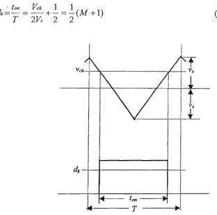
This voltage is transferred to a voltage/trigger converter, where it is compared with a triangle waveform. T h e intersections determine the switching pattern of Fig. 2.3. If the switching frequency is high enough, the voltage Vck can be treated as a constant within the
switching period, and the trigger duty ratio dk will have the following relationship to Vch
where M i s modulation index.
• ton Vck 1 1
dk=— = + — = — (M + 1)
T 2V.s 2 2
(2.3-5)
Fig. 2.3 The Waveform of Voltage Trigger Converter
Thus combining the relation of (2.3-4) and (2.3-5) the required P C F F control law of (2.3-1) is realized. If Vik is A C terminal voltage of converter, Vik can be expressed by:
3 J 3
io = Y1 dk ik = y /AFC*
^ * * 2Vs j£
(2.3-7)
*=1
2.3.2 P C F F C O N T R O L S Y S T E M IN R O T A T I N G F R A M E O F R E F E R E N C E [19]
The PCFF control system is nonlinear and time-variant system. Therefore, analysis and design of PCFF system is quite complex. The PCFF A C / D C voltage source converter in a
stationary frame of reference has been derived, rewritten from (2.2-10) and (2.3-1).
ZX = AX + Be
where: L 0 0 0 0 L 0 0 0 0 L 0 0" 0 0 C B = 1 0 0 0 0 1 0 0 0 0 1 0 0" 0 0 1 R~o_ X l\ h Vd e\ ei ei A = (2.3-8)
-R 0 0
0 -R 0
0 0-/?
d\ d2 di
(dx-\JTdk)
k = \ •(rf2-Ij>)
-> k=\
{dy-H^dk)
-> * = i
J_
Ro
dk = — Vd
ek-(R )ik M 1 + — 2
(2.3-9)
If a sinusoidal line current is required, the reference current should have the form:
Ick = 1cm COS 6)t + 0c-(k-l)
2JZ
(2.3-10)
CHAPTER 2. THE PRINCIPLE OF PCFF CONTROL 22
synchronized with the utility frequency co [19]. T h e transformation matrix T and its
inverse matrix T~
xare:
T =
s
1
1
1
0
-ja*e
•i 2*\ -Aa*-—,e
3 .. 2nse
30
jcot
e
., 2n. j(col——)
e
3 ., 2n. J(ax+—)e
30
0
0
0
V3"J
-1T
1
S
1
e
-jote
0
l
e
3e
30
l
2a-,
e
3e
30
0
0
0
V3
Thus, the state variable vector in the Totating frame X
rand the vector in the stationary frame
X h a v e the relation:
X=TX
r(2.3-11)
W h e r e Xr =
laif
h
Vd
and its differentiation:
X
= TX
+T
Xr(2.3-12)
W h e r e /„, i, and i
hare zero sequence current, forward current and backward current
relatively. Pre-multiplying by ^
_1on both sides of (2.3-8) yields:
{T~ X
ZT)Xr = {T-'AT-T-'ZT)X + T- Be
(2.3-13)
B y substituting (2.3-8) and (2.3-9) into (2.3-13), the following time-invariant state space
equation in the rotating frame of reference can be obtained:
•
Lio
Lif
•Lib
•CVd
R
0
0 jcoL
Is
0
o
042
0
0
jcoL
-«43
L_
Ts
0
0
0
J_
lo if ib Vd+
0
SLe~
ja2Ts
SLe
j(k2Ts
ei~Ro
• Icm-Icm
(2.3-14)
where
an
Vd
S(
em-(R )/*•
2 Ts
SL
lent,./ft
#43 = •
Vd
V3<
em•(*-£»•
V3I
Zcm ,y«27;
For a three-phase system without neutral line, the zero sequence current L is equal to zero. The equation (2.3-14) can be simplified to its reduced form:
Li/ Lib CVd = icoL T 0 #42
jcoL L_
T (341 0 0 Ro
u
Vd +SLe~
J& 2TsSLe
j(k • Icm 2Ts ei.Yo
• Icm (2.3-15)
2.4 THE MODEL OF PCFF CONTROL SYSTEM
O n e of the most important tasks in the analysis and design of control system is mathematical model of the system. The differential equation (2.3-15) is a nonlinear equation. It can be approximately linearized within a small area around the DC operating points.
2.4.1 D C M O D E L
Let the state variables be expressed as:
if ib Vd =
If
lb Vd+
Az> AM AK/ (2.4-1) the inputs the load the controlem — Em + Ae?«,
Ao = Ro + Al"o ,
Icm — Jem + A/cm
CD = Q + A<S)
ei = EL + Aei
C H A P T E R 2. T H E PRINCIPLE O F PCFF C O N T R O L 24
jQL-0
,442
Ts
0
jQL- —
Ts0
0
J_
Ro 'If h Vd + \l3Le-JA 2Ts sl3LejBc 2TX Ro-0
(2.4-2)where
^42
Vd
\3Ern . L.T *j3LIcm /ft
(R )Ib : -£.J _
2 Ts 2Ts
AAI = — y/3Em L. -43LIcm _j&
(R )// :—e
2 T./ 2Ts
T h e steady-state solutions can be obtained directly from the D C model. F r o m the first row of (2.4-2), the steady-state forward current component 1/ can be obtained as
If
// =
Slcme-
j8c2Q.-jQTs)
9
S= tan
-1(Oft)
(2.4-3)
(2.4-4)
And
Kr = yll + (QTs): (2.4-5)Then '/ =
SLn,e-m
-
a)2KT
(2.4-6)
Similarly, the steady-state backward current component h can be obtained from (2.4-2) as
/* =
2KT
(2.4-7)
The steady-state D C output Va can be calculated from the third r o w of (2.4-2) as
Vd = HEL
+lEi
2+^0-[E
mKrco^e
c-e
s)-RI
cJ\ (2.4-8)
If the leading compensation angle Oc is adjusted to be equal t o 0 „ then
Vd = (2.4-11)
The steady-state current solution I/, h are the components of the line current in the rotating frame of reference, but the variables of greatest concern are the steady-state peak current Im and the power factor <J>. They can be derived as follows:
% •
K
r<J> = Arg(If) = (0s-0c)
(2.4-12)
(2.4-13)
The approximation KT = IJI + (QTS)2 » 1 is generally valid, because the switching frequency of the converter is usually m u c h higher than the supply frequency. The steady-state peak current Im is approximately equal to the control current 1^, and the power
factor angle O is equal to 0° if the leading compensation angle is adjusted to be
6C = # , =tan
_1
(Q7^v). Therefore, one advantage of the P C F F control is its input power factor, which is automatically maintained at unity if 6C = 6S. The only control variable icm
can be used to regulate the D C output voltage. The P W M converter under the P C F F control becomes a single-input signal-output system.
2.4.2 A C M O D E L
The AC model of the converter under PCFF control can be derived by substituting the equation (2.4-1), the inputs, load and control into (2.3-15).
Z'AX = AxAXr + AcAicm + Ao>Aco + AeAem + ArAro + ALAei (2.4-14)
r
AcAUm, {AaAa + AeAem) and (ArAro + AhAei) are control, input disturbances and load
disturbances terms respectively, where
Zr =
~L
0
0 L
0 0
0"
0
C
AXr = Ai/
Ah
AVd
Am =
jLI/
-JLL
0
AL =
0 0
l_
CHAPTER 2. THE PRINCIPLE OF PCFF CONTROL 26
Ax =
jQL
0
Ts
0
jQL- L_
Ts
0
0
A42- — (R-—)h AAI- — (R-—)I/
Vd Ts Vd T
(Aul/ + Aillb) Vd Ro
Ac =
y/3L
(
27/,
SL
2Ts
-jBc
,J&
L(^LXe
J*Jr + e-
J*I.)
Vd 2Ts
Ae =
2Vd
0
0
(// + /*)
Ar =
0
0
(IVd-EL)
Ro2
F r o m the A C m o d e l derived in (2.4-14), the Laplace transformation of the variable vector
AXr(s) can be written as
AXr(s) = (sZr - Ax)~x (AcAlcm + AoA(D + AeAem + ArAro + ALACL) (2.4-15)
Equation (2.4-15) gives all the transfer functions between the state variables Ai/, Ah, AVd
and the control Aicm, input disturbance Aco, Aem or load disturbance Ar„, Aei,, and the
small signal transfer function from any disturbance or control to any state variable can be
derived from them.
T h e transfer function — ^ - ^ can b e obtained by setting Aco = Aem -Ar0 = Aet = 0 in
Aicm(s)
(2.4-15). Then,
AXr(s)
Aif(s)' Ah(s) AVd(s)
= (sZr - Ax) ' AcAicm(s) (2.4-16)
T h e third r o w of this equation gives the transfer function / . It has two zeros and
Alcm(s)
three poles, but since the converter usually works at the condition of KT = ^\ + (QTs)2 « 1
AVdjs) ^ 3{E,„-2LmR-LLms)(\ + sTs) _ 3{Em-2LmR)
Aicm(S) ~
(
\-s Lla
Em — AlcmR
2Vd(l + sTs)' + sC 2Vd
( Ei^
2 —
Vd_ Ro
(1 + sTs)
n (2.4-17)
\ + s- CRo
It is seen that one pole and one zero are canceled. This is another advantage of P C F F
control. The transfer function has a lower order and can be rewritten as
(
AVdjs) Aicm(s)
= AV
^
CD o J
1+
CD pi
1 +
CD Pi J(2.4-18)
where
KP =
3{Em-2IcmR)
CD,,
-Em — 2 icm A
LiLcm
">* =
2 - ^
Vd_RoC "2 Ts
It can been seen from (2.4-18) that, there is a zero in the right-half s plane. Hence, the
transfer function is of the non-minimum phase type.
2.4.3 TRANSFER FUNCTION BETWEEN PEAK LINE CURRENT AND CONTROL SIGNAL
Since peak link current A/» is not one of the variables in the rotating frame of reference, it
is necessary to find the relation between the variables Ai/, An, and control A/™ first. It is
known that
im = —j= iji/ • ib
V3
(2.4-19)
since
Im — Im + Aim , i/ = 1/ + Ai/, ib = h + Aib
CHAPTER 2. THE PRINCIPLE OF PCFF CONTROL 28
f(x,y) « /(*»,yo) + ^-(x-x0) + ^-(y-y0) ox oy
Therefore
/„ = -j=<JlfI>
(2.4-20)and
Ai«
S
—Ai/ + J—AhIf V A
(2.4-21)
F r o m (2.4-6) and (2.4-7), it is seen that
'r
e
y(A-A)
/ A =
e
-v'(
ft-
ft)
and
Az'«. (5) 1
Aicm(s) S
e.W-&) Ai/(s) y^ft) A M ( S )
Aicm(s) Alcm(s)
(2.4-22)
T h e t w o functions - — ^ — and — can be derived from the first and second rows of Aicm(s) Aic,,,(s)
(2.4-16) as
Ai/(s) V 3 e ja.
Aicm(s) 2 (sTs-jQTs + \)
Ah(s) V3 e
j*
Aicm(s) 2 (sTs-jQTs + l)
Substitution of these into (2.4-22) yields
Aim(s)
cos
(9.. - tan
•1
QT(1+sTs)
A/»(J) V(
1+ -
y 7 ;)
2 +(
Q 7 ;)
:(2.4-23)
For the frequency range co « —
Is
tan"
Q7;
(1 + sTs)
«tan"1 Q7/, = <9,,
cos
0 -tan" QTs(1-sTs)
- ^ 0 « _ J — (2.4-24)
Aicm(s) 1 + STs
From this transfer function and the steady-state solution with Im « Lm, it is concluded that
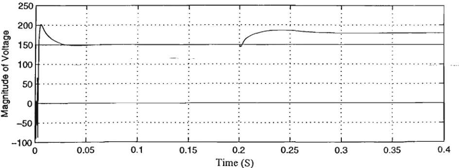
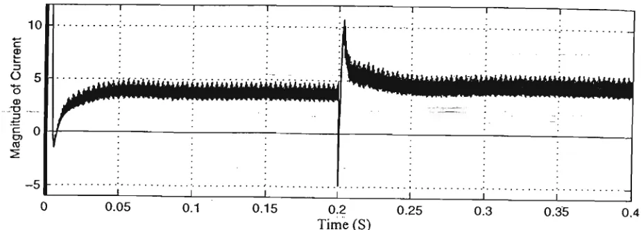
the peak line current im would follow the control icm with a nearly first-order lag depending
only on the switching frequency Fs- —. Because the switching frequency usually is Is
CHAPTER 2. THE PRINCIPLE OF PCFF CONTROL 30
2.5 SUMMARY
1. A comprehensive analysis of the PCFF control is provided, including a steady-state analysis, a dynamic response analysis and their solutions.
2. The derived solutions show that the line current follows the control signal closely with a nearly first-order lag, depending on the switching frequency. Because the switching
frequency usually is rather high, the system has a rather good dynamic response.
3. The PCFF control only has one control variable. The power factor is maintained at unity if the leading compensation angle is appropriately adjusted. T h e control signal can be then used to regulate the D C output voltage. Therefore, the converter under P C F F control becomes a single-input, single-output system.
4. From the derivation of transfer function relating DC output voltage to control signal, it is seen that one pole has been cancelled by a zero. Hence, the system has a low order
Chapter 3
T H E D E S I G N O F Hoo C O N T R O L L E R
3.1 INTRODUCTION
The model of the P C F F control system is derived, and the comprehensive analysis is given
in Chapter 2. T h e P C F F control scheme has a fast dynamic response, a well-defined
switching pattern, and low complexity. However, the major problem with the P C F F
scheme is its sensitivity to parameter variations of the system. Hence, the system
performance m a y deteriorate w h e n operating conditions of the system are changed. For
example, from the rectifying m o d e to the regenerating m o d e , or w h e n the system is subject
to load disturbances. T h e difference between a real system and its mathematical model is a
source of uncertainty, which directly degrades the performance of the P C F F controlled
system. T h e requirement of coping with uncertainty for the P C F F scheme is a robustness
problem and can only be compensated by a properly designed D C voltage regulator.
The conventional design approach to the DC voltage stabilisation utilises a proportional and
integral (PI) controller operating on an error signal V<j ref - Vd. Although theoretically a PI
controller is comparable to any other controller for a single-input single-output system, its
design method is based o n a trial and error procedure, and the optimal solution is not easy
to be obtained.
In this project, an advanced Hn controller is proposed in the place of a PI voltage
regulator. N o t only the Hn theory has its unique approach to the uncertainty issue, but also
its design method allows both the stability robustness and performance robustness to be
considered at the design stage [29-34]. The HK voltage regulator is to work with the P C F F
current control to compensate uncertainty problem. T h e successful introduction of Hm
CHAPTER 3. THE DESIGN OF H CONTROLLER
32
3.2 T H E P R E L I M I N A R Y OFHoo C O N T R O L T H E O R Y
Control theory is concerned with the control of processes with inputs and outputs. H o w can
a desired goal be achieved for outputs of a plant by choosing a control input?
The first step is to find a mathematical model describing the behavior of the real plant.
Since the mathematical model should be simple enough for the mathematical tools, the
model is not able to describe exactly a real plant. Because of this, the real-time behavior
might differ significantly from the mathematically predicted behavior. Therefore, it is
extremely important that a control method is chosen for the mathematical model, which
deviates from the real plant. This leads to the so-called robustness analysis of the
mathematical model and a robust controller is to be designed to cope with this deviation.
Robustness of a system says nothing more than that the stability of the system will stand
against perturbation.
Since the last decade, the H^ norm as a measure system has been thoroughly embedded in
control theory, and there has been a gigantic surge in research efforts towards the
minimization of the H
xnorm for a closed-loop system to cope with model uncertainty. A
fairly complete solution is n o w available.
3.2.1 SINGULAR VALUES
The singular values of a rank r matrix^, denoted yA,. are the non-negative square-roots of
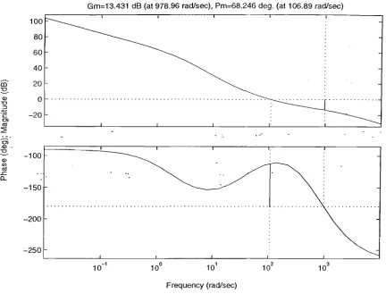
the eigenvalues of A *A [29], such that
< J , = W (i=U,...r) (3.2-1)
The greatest singular value a, is denoted by a, and least singular value is denoted by a
The properties of singular values are:
(1) a(A) = max Lfl
=max||v4x|| a(A) = min V? =
mHHI where lixll= JTx
~° IM ft - ~° M pp.
(3)a(AB)<cr(A)a(B)
(4) a(A + B)< a(A) + a(B)
(5) a(A) + cr(AA) > cr(A + AA)> a(A) - a(AA)
3.2.2 SPACES, H^AND HL NORMS
The HK space is the class of matrix-valued functions which are analytic and bounded in the
open right half-plane, the Hx norm of such a function, say F(s), being defined as
\\F\l:= sup cr[F(s)] (3.2-2)
Here a[F(s)] denotes the greatest singular value and the supremum is over all s in the open right half-plane, Res > 0 [30]. For such a function the boundary value
F(JCD) := lim F(£ + JCD) (3.2-3)
exists for almost all co and the boundary function is of Lx space. As a consequence of the
maximum modulus principle the HK norm of F(s) equals the Lm norm of the boundary
function, i.e.,
\\F\l:= ess sup a[F(jco)] (3.2-4)
m
For example, suppose F(s) is scalar-valued, analytic and bounded in Res>0, and
continuous on the imaginary axis, then IF^ equals the distance in the complex plane from
the origin to the farthest point on the Nyquist plot of F. The space L2[0,co] is the class of
vector-valued square-integrable functions. The norm on Z2[0,oo] is
(3.2-5)
Where * denotes complex-conjugate transpose. The Laplace transform of x(t) in Z,2[0,«>],
denoted by x(s), belongs to the H2 space of functions analytic in Res > 0 and H2 norm is
CHAPTER 3. THE DESIGN OF H „ CONTROLLER
34
n -•= <?*)
-1 jx(Jcv)* x{jco)dcD (3.2-6)Suppose F G H„ . Then Fx G 772 whenever x e H2 and moreover
\\F\l=sup{\\Fx\\2:xeH2,\\x\\2=l} (3.2-7)
Therefor it can be concluded that
1. The space H„ is the class of all stable matrix-values functions.
2. The space H2 is the class of Laplace transform of bounded input and bounded
output signals.
3. Hm norm represents the energy gain.
3.2.3 STANDARD REPRESENTATION FOR EL PROBLEM
The standard configuration for //„, optimal design [34] is shown in Fig. 3.1, where (v) is an 'external inputs' vector of all the signals entering the system, including load disturbance, sensor noise, reference input and so on. (z) is an 'error' vector of all the signals required to characterize the behaviour of the closed-loop system, for example, it can be error signals, weighted control output and so on. Both these vectors m a y contain elements which are abstract in the sense that they m a y be defined mathematically, but do not represent signals which actually exist at any point in the system, (w) is a control vectors, and (y) is the vector of measured outputs. The matrix K(s) is the controller to be designed.
©
u
^
w
w
P(s)
K(s)
M^
y
fc,
w
Fig. 3.1 Standard Configuration
P(s) is a transfer matrix derived from the nominal plant model. However, it m a y also
include weighting functions which depend on design problems to be solved. Suppose that
P(S) =
P2i(s) P22( s
)
(3.2-8)
So the equations corresponding to the system of Fig. 3.1 can be derived as follows:
z
= Puv + Pnu
y = P^v + P22u (3.2-9)
u = Ky
The transfer matrix from v to z is denoted as M(s), which can be obtained from the last equation where p22 is strictly proper and real rational.
M(s) = pu + puK(I- p22K.y p2l (3.2-10)
The objective of Hx design is to determine a proper and real rational controller K, which
can not only stabilize the closed-loop but also minimize the Hn norm of M(S). In other
words, Hm design is to solve the following optimal problem.
min \\M(s)\\ (3.2-11)
This is known as the Hm optimization problem. In the design, weighting functions are
introduced to normalize M(s) . The weighting function expresses the relative importance of different frequencies (it is bigger for frequencies whose presence is more disturbing). By adjusting the weighting function, better performance at frequencies concerned can be obtained.
3.2.4 THE Hog PROBLEM FORMULATION
• CONDITION OF STABILITY ROBUSTNESS
When the uncertainty AM(s) is expressed in the multiplication form as shown in Fig. 3.2.
The true plant transfer function is written as [34]:
G(s) = [l + AM(s)]G0(s) (3.2-12)
Where, the effect of AM (s) on the performance of a closed-loop system over the high