Micro Data Handling for nm Range Semiconductor
Device Using High Resolution ADC
Meenal M Ratnparkhi
1, Minakshee M Patil
2PG Student [Digital Systems], Dept. of E & TC, Sinhgad Academy of Engineering, Pune, India1 Assistant Professor [VLSI], Dept. of E & TC, Sinhgad Academy of Engineering, Pune, India2
ABSTRACT: In VLSI technology devices are fabricated using semiconductor materials like Si, GaAs have been scaled down in nm range. For these devices there is a need to monitor the voltage in µV range. The proposed work aims at measuring voltage and data logging application with real time facility. This will help to understand the characteristics of nm range devices. The work will also focus on nm sensors and devices testing. The proposed work will use Resistive method. This method is a linear and accurate for measuring current. In this resister is inserted in series with the current path and the voltage drop across it measured. We can determine the voltage by applying Ohms law. Design contains very high precise (∑-∆) ADC with very good conversion speed. Microcontroller based µV data logging real time system will be cost effective for such application with its limitations. Design includes the facility of memory card for data storage.
KEYWORDS: Data logging; real time system; high resolution ADC; nm range; resistive method; semiconductor devices.
I.INTRODUCTION
Digital Multimeter (DMM’s) are usually used to measure current, voltage signal levels greater than 100µA, 100µV and resistance less than 1GΩ. For signal levels below the ones mentioned more sensitive instruments are required such as picoammeters and nanovoltmeteres. The noise generated by resistance present in the circuit or source leakage determines the sensitivity of the device [9].
There are basically three methods for current measurement depending on the application: resistive, optical-resistive and magnetic.
A. Resistive method
The resistive method is a linear and accurate method for measuring current. In this method resistor is series with the current path and measures the voltage drop across it and the current can be determined by applying Ohm’s law. The advantage of resistive method is that it is a reliable method. This method is having no offset i.e. for zero input it gives zero output. No external power is required for this method. This method is frequency independent method. By using this method we can able to measure AC as well as DC current [1][11].
B. Optical-resistive method
This method uses a sensing resistor and an optoisolating device for measuring the current value. The optocoupler simply transfers the already measured current information across a galvanic isolated barrier. The received signal then processed by an ADC of a microcontroller and transformed into an actual current value. Using the optical method provides a low cost solution for applications where isolation is required however this is a relatively low speed solution. The main advantage of this method is low input common mode voltage, ground referenced input and output and a low cost solution [2].
C. Magnetic method
measurement of high currents is required. The disadvantage of this method is that it measure only AC current. Also output is frequency dependent [2].
To measure low current i.e. in the µA range we select resistive method. Because we are focusing on the range low and the medium current so this method is suitable for this range.
Also for the high resolution we are using 24bit sigma-delta (∑-∆) ADC. This ADC is used because it is having low bandwidth, low cost low power and high resolution.
The rest of the paper is organized as follows: section II describes the resistor current measurement method, section III provides two point probe measurement, section IV gives a detailed description of the system architecture, V ADC selection, VI results and section VII concludes this paper.
II. RESISTOR CURRENT SENSING METHOD
Current sensing resistor
In this method device detect and converts current to measured output voltage, which is proportional to current through the measured path. A current sensing resistor is the most commonly used. It can be considered a current to voltage converter, where inserting a resistor into the current path, the current is converted into linear way
V = I × R (1) The main advantages of current sensing resistive method are
Advantages: - Low cost
- High measurement accuracy
- Measurable current range from very low to medium - Capability to measure DC or AC current
Selection criteria
The voltage drop across the sensing resistor may become low enough to be comparable to the input offset voltage of subsequent analog conditioning circuit, which would compromise the measurement accuracy. The current sensing resistor inductance must be low. For the current monitor following selection criteria’s are consider-
1. Resistance must be low having tight tolerance 2. High current capability
3. It should have low thermal EMF, low temperature coefficient.
Depending upon the application there are two type of current sensing technique 1. Low side current sensing
As shown in fig.1 the sensing resistor is between load and ground. The sensed voltage is very small. So this voltage is given to the Op-Amp circuitry to get measurable output VOUT. The main aspect of this sensing is that the common mode voltage rang of the Op-Amp must be include ground. In this technique short circuit detection not required also ground disturbance can be tolerated.
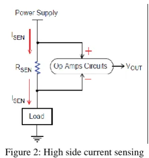
2. High side current sensing
Figure 2: High side current sensing
As shown in fig.2 the sensing resistor is connected between power supply and load. The sensed voltage is amplified further. [3]
III. TWO POINT PROBE MEASUREMENT
The probe tips are made of tungsten carbide. Each tip is mounted on the end of separate arm. The probe tips are shape such that they can be positioned to each other. The tips are separated by 20µm. the probe tips are lowered onto the sample as gently as possible. [6] If the contact area of the probes small enough, the largest component of the measured resistance arises from the current is having following relationship:
Rs =
2𝑎𝜌(2)
Where,
Rs = the measured spreading resistance in ohm
ρ = the local resistivity in ohm-cm
a = the radius of the contact area of the probes in cm
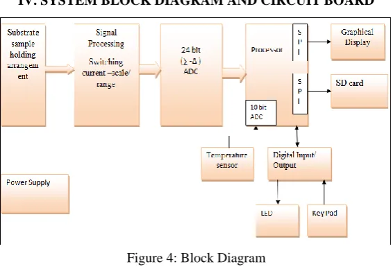
IV. SYSTEM BLOCK DIAGRAM AND CIRCUIT BOARD
Figure 4: Block Diagram
Power supply - For this we require very low noise power supply. If the noise in the supply is large then this noise may affect data. In this project noise level must be reduced up to 100µV.
Substrate sample holding arrangement - In nano technology research we do different types of deposition on Si wafer. To measure the IV characteristic and resistivity we supply known amount of voltage and with different steps we increase the current gradually to get IV characteristic. For connectivity with the substrate we get probe station.
Signal processing - In this section current sensing circuit is used to sense the current in µA. Depending on the output signal of the substrate we are going to built op-amp circuit. This section is used to amplify the signal which comes from sensing section. Also in this section we are designing switching circuitry for range selection.
Analog to digital converter - In this the signal which came from signal processing section is converted into digital form. An ADC takes analog voltage levels as an input and samples the voltage level at a certain rate. Each sample is compared to a reference voltage and categorized as a digital number proportional to the inputs amplitude at the time of the sample. To get an accurate data representation of the analog input the A/D sample rate must be very fast. In this section we are using high resolution precise ADC for data conversion with high speed. Data conversion is in real time. For this sigma-delta (∑-∆) ADC is used. Its accuracy level is high. It is extremely high-performance and low noise ADC. The output data word is provided as either a 24-bit word, allowing complete utilization of the inherently high resolution.
Microcontroller- For this project we require very high speed controller. Digital signal is processed in this section and forward it to the display. For correct data conversion we required temperature coefficient. So to calculate the room temperature we connect the internal ADC of microcontroller to the temperature sensor. In this section we are using PIC processor, which contains inbuilt ADC. The output of the temperature sensor is given to the ADC. It also contain inbuilt Serial Peripheral Interface (SPI) interface. This is used to communicate with the graphical display also for SD card interface. The processing speed of microcontroller is higher than the conversion speed of ADC. Hence there is a possibility that the microcontroller remains idle till the next ADC data arrives.
Temperature sensor- In semiconductor devices the current is affected by temperature. As temperature increases the current decreases because semiconductor devises have negative temperature coefficient. Therefore to sense the room temperature this temperature sensor is connected.
Digital I/O section- In this section we are providing keyboard for following inputs
Reset the system
Output of graphic display (graph/reading)
SD card- It is used for data storage, so that even though the user in not present in that room system can record the data. Also the stored data can be observed by simply connecting this SD card to the computer. Fig. 5 shows the system circuit board.
Figure 5: System circuit board
V. ADC SECTION
This project is focusing on very low range to mid range voltage and current i.e. the range is micro and above. For this range we require very high resolution. For selection of the ADC we must consider that the step size must be very small then only we can able to measure such low current. Considering that we are selecting 24 bit sigma-delta (∑-∆) ADC.A Sigma-Delta ADC works by over-sampling, where simple analog filters in the Sigma-Delta (∑-∆) modulator shape the quantization noise so that the SNR inthe bandwidth of interestis much lower than would otherwise be the case, and by using high performance digital filters and decimation to eliminate noise outside the required pass band. Because the sampling operation in a sigma-delta (Σ-Δ) occurs at the output of the loop filter, the performance impact due to errors in the sampling operation will be greatly reduced. [5]
For the above application we selected ADC ADuCM360. The ADuCM360 is a fully integrated, 3.9 kSPS, 24-bit data acquisition system that incorporates dual high performance, multichannel sigma-delta (∑-∆) analog-to-digital converters (ADCs). The ADCs contain two parallel fitters a sinc3 or sinc4 fitters in parallel with a sinc2 fitters. The sinc3 or sinc4 fitter is used for precision measurements. The sinc2 fitter is used for fast measurements and for the detection of step changes in the input signal.
V. RESULT AND DISCUSSION
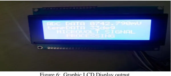
Figure 6: Graphic LCD Display output
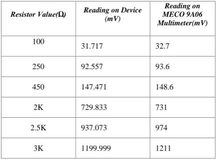
Table1: Observed reading on Device and on MECO 9A06
Resistor Value(Ω) Reading on Device (mV)
Reading on MECO 9A06 Multimeter(mV)
100
31.717 32.7
250 92.557 93.6
450 147.471 148.6
2K 729.833 731
2.5K 937.073 974
3K 1199.999 1211
It was observed from the Table.1 that our device give precise reading as compare to measuring device. The graph shows that there is linear relationship between our device and the actual voltage. This accuracy is achieved by using 24bit sigma-delta (∑-∆) ADC. Accuracy is obtained up to 100µV.
Figure 7: Accurate linearity of actual and linear voltage in µV
VI.CONCLUSION
The proposed device can be used to measure particular range of resistivity with effect of noise under consideration. The IV characteristic of the device on the Si chip can also be measured effectively. The room temperature also affects the Si devices. The temperature is observed by using temperature sensor. This will increase accuracy of measured value. Higher accuracy in measurement of current can be achieved using 24 bit high precision sigma-delta (∑-∆) ADC. All the measured parameters are displayed using graphical LCD display which leads in simplicity and ease of use. The entire work processes a low cost solution over the existing methods of current measurement.
As future work directions we plan to achieve more accuracy. To achieve more accuracy we redesign the power supply section to reduce the noise. So we can remove the inductive noise and the noise generated by the regulator IC’s.
0 200 400 600 800 1000 1200 1400
0 500 1000 1500
A
ctu
al
Vo
ltage
(µ
V)
REFERENCES
[1] Bode P.A., “Current Measurement Application Handbook”, Issue 5, Zetex Semiconductor, January 2008.
[2] Cirstea Cosmin, Cernaianu Mihail and Gontean Aurel, “An Inductive System for Measuring Microampere Currents”, International Symposium for Design and Technology in Electronic Packaging, pp.197 - 200, 2012.
[3] Zhen Yang, ”Current sensing circuit concepts and fundamentals” Microchip Technology Inc.
[4] Wolpert D. and Ampadu P. “Managing temperature effect in nanoscale adaptive system” Springer, vol. 1, 2012. [5] “Continuous-Time Sigma-Delta ADCs”, Texas Instrument, Literature Number: SNAA098
[6] Brennan Roger and Dickey David, “Determination of diffusion characteristics using two- and four-point probe measurements”, 2001. [7] Gayakwad Ramakant,“Op-Amps and Linear Integrated Circuits”, 4th Edition, PHI Learning, 2010.
[8] Sarma V. and Sahoo B., “Pipelined adc based design of bandpass sigma-delta adc,”Electronic Letters,Vol.49, pp.646-648, 2013.
[9] Keithly, Low Level Measurements Handbook – “Precision DC Current, Voltage and Resistance Measurements”, 6th Edition, Keithley Instruments, 2004
[10] Tapan Kr, Maiti and Kar Asim, “Novel Remote Measurement Technique Using Resistive Sensor as Grounded Load in an Op-amp Based V-to-I Converter”, V-to-IEEE SENSORS JOURNAL, VOL. 9, NO. 3, pp.244-245, MARCH 2009.