c e-ISSN: 2348-6848, p- ISSN: 2348-795X Volume 2, Issue 12, December 2015
International Journal of Research (IJR)
Available at http://internationaljournalofresearch.org
Encoding Scheme for Power Reduction in NOC Links
Gorantla Anuja
1& V.T.Venkateswarlu
21
PG Scholar(VLSI&ES), Vasireddy Venkatadri Institute Of Technology, Guntur, Andhra Pradesh.
2
Assistant Professor, Dept of ECE, Vasireddy Venkatadri Institute Of Technology, Guntur ,Andhra Pradesh.
ABSTRACT:
This paper focus on techniques aimed at decreasing the power loss by the network links. In fact, the power loss by the network links is as equal as that loss by routers and network interfaces (NIs) and their difference is expected to increase as technology scales As technology shrinks, the power loss by the links of a network-on-chip (NoC) starts to release with the power loss by the other aim of the communication subsystem, namely, the routers and the network interfaces (NIs). In this paper, we present a set of data encoding techniques aimed at reduce the power loss by the links of an NoC. The proposed work is general and clear with respect to the essential NoC fabric.
Index Terms—Coupling switching activity; data encoding; interconnection on chip; low;
1.Introduction
Network on chip is an emerging approach for the design of on chip communication architecture. A network on chip communication gives resistance in the topology, in support to that the flow control, advance routing algorithms, self switching techniques guarantying the quality of service. System on chip is an departure to design the communication system between property cores in a system. The communication in system on chip uses dedicated buses between communicating resources. This will not give any resistance since the needs of the communication, in each case, have to be thought of every time a design is made.
2.Overview of Proposal
The basic concept is to apply the encoding technique in end-to-end links in resource network interface of wormhole routed network on chip. The most suitable switching technique for on chip communication is wormhole switching.
Figure 1. General Scheme of proposed approach The channel nature is the basic concept for the wormhole switching. The links of the routing path are cross by the same interruption of flits, the encoding technique ensure the same switching behavior in each routing path. The encoder and decoder blocks are incorporated in the network interface. The encoder encodes the outgoing flit in the packet in such a way that the power dissipated is minimized by inter router point to point links which form the routing path.
c e-ISSN: 2348-6848, p- ISSN: 2348-795X Volume 2, Issue 12, December 2015
International Journal of Research (IJR)
Available at http://internationaljournalofresearch.org
In this section, we present the proposed encoding techniques whose goal is to decrease power loss by minimizing the coupling transition activities on the links of the interconnection. Let us first explain the power model that contains different components of power loss of a link. The dynamic power lossed by the interconnects and drivers is
P = [T0→1 (Cs + Cl ) + TcCc]
V2ddFck……….. (1)
Where T0→1 is the number of 0 → 1 transitions in the bus in two consecutive transmissions, Tc
is the number of correlated switching between physically adjacent lines, Cs is the line to substrate capacitance, Cl is the load capacitance,
Cc is the coupling capacitance, Vdd is the supply voltage, and Fck is the clock frequency. The effective switched capacitance varies from type to type, and hence, the coupling transition activity, Tc, is a weighted sum of different types of coupling transition contributions .Therefore
Tc = K1T1 + K2T2 + K3T3 + K4T4 ……….. (2)
Where Ti is the average number of Type i
transition and Ki is its corresponding weight. We use K1 = 1, K2 = 2, and K3 = K4 = 0. The occurrence probability for a random set of data is 1/2 and 1/8, respectively. This leads to a higher value for K1T 1 compared with K2T 2 suggesting that minimizing the number of transition may lead to a considerable power loss. Using (2), one may express (1) as
P = [T0→1 (Cs + Cl ) + (T1 + 2T2) Cc] V
2ddFck………... (3) According to [3], Cl can be neglected
P ∝ T0→1Cs + (T1 + 2T2)Cc……… (4) Consider that flit (t − 1) and flit (t) refer to the previous flit which was transferred via the link and the flit which is about to pass through the link, respectively. Note that the first bit is the value of the generic ith line of the link, whereas the second bit represents the value of its (i +1)th line. In the rest of this section, we present three data encoding techniques designed for reducing
the dynamic power loss of the network links along with a possible hardware implementation of the decoder.
A. Scheme I
In scheme I, we focus on reducing the numbers of Type I transitions (by converting them to Types III and IV transitions) and Type II transitions (by converting them to Type I transition). The scheme compares the current data with the previous one to decide whether odd inversion or no inversion of the current data can lead to the link power reduction.
1) Power Model: If the flit is odd inverted before being transmitted, the dynamic power on the link is
P_ ∝T _0→1+ _K1T _1+ K2T _2+ K3T _3+
K4T _4_Cc ………..(5)
where T _0→1, T _1, T _2, T _3, and T _4, are the self-transition activity,and the coupling transition activity of Types I, II, III, and IV,respectively. Table I reports, for each transition, the relationshipbetween the coupling transition activities of the flit when transmitted as is and when its bits are odd inverted. Data are organized as follows. The first bit is the value of the generic ith line of the link, whereas the second bit represents the value of its (i + 1)th line. For each partition, the first (second) line represents the values at time t − 1 (t). As Table I
shows, if the flit is odd inverted, Types II, III, and IV transitions convert to Type I transitions. In the case of Type I transitions, the inversion leads to one of Types II, III, or Type IV transitions. In particular, the transitions indicated as T 1* , T 1** , and T1*** in the table convert to Types II, III, and IVtransitions, respectively. Also, we have T _0→1= T0→0(odd)
+T0→1(even) where odd/even refers to odd/even lines. Therefore, (5) can be expressed as
P ∝ _T0→0(odd) + T0→1(even)_Cs
+[K1 (T2+T3+T4)+K2T 1***+K3T1*+K4T
c e-ISSN: 2348-6848, p- ISSN: 2348-795X Volume 2, Issue 12, December 2015
International Journal of Research (IJR)
Available at http://internationaljournalofresearch.org
Thus, if P > P_, it is convenient to odd invert the flit before transmission to reduce the link power dissipation. Using (4) and (6) and noting
that Cc/Cs = 4 [26], we obtain thefollowing odd invert condition
1/4T0→1 + T1 + 2T2 >1/4_T0→0(odd) +
T0→1(even)_+T2 + T3 + T4 + 2T1***
.
Figure2. Encoder architecture scheme I. (a) Circuit diagram . (b) Internal view of the encoder block (E).
which is the exact condition to be used to decide whether the odd invert has to be performed. Since the terms T0→1(odd) and T0→0(odd) are weighted with a factor of 1/4, for link widths greater than 16 bits, the misprediction of the invert condition will not exceed 1.2% on average [23]. Thus, we can approximate the exact condition as
T1 + 2T2 > T2 + T3 + T4 + 2T1***……... (8)
Of course, the use of the approximated odd invert condition reduces the effectiveness of the encoding scheme due to the error induced by the approximation but it simplifies the hardware implementation of encoder. Now, defining
Tx = T3 + T4 + T1 and
Ty = T2 + T1 − T1 ***……….(9) one can rewrite (8) as
Ty > Tx …….. (10)
Assuming the link width of w bits, the total transition between adjacent lines is w − 1, and hence Ty + Tx = w − 1……… (11)
Thus, we can write (10) as
Ty >(w − 1)/2……….. (12)
This presents the condition used to determine whether the odd inversion has to be performed or not.
B. Scheme II
c e-ISSN: 2348-6848, p- ISSN: 2348-795X Volume 2, Issue 12, December 2015
International Journal of Research (IJR)
Available at http://internationaljournalofresearch.org
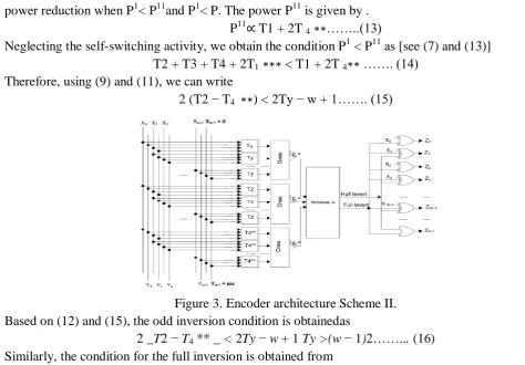
Power Model: Let us indicate with P, P1, and P11 the power dissipated by the link when the flit is transmitted with no inversion, odd inversion, and full inversion, respectively.The odd inversion leads to power reduction when P1< P11and P1< P. The power P11 is given by .
P11∝ T1 + 2T 4∗∗……..(13)
Neglecting the self-switching activity, we obtain the condition P1 < P11 as [see (7) and (13)] T2 + T3 + T4 + 2T1∗∗∗ < T1 + 2T 4∗∗ ……. (14)
Therefore, using (9) and (11), we can write
2 (T2 − T4 ∗∗) < 2Ty − w + 1……. (15)
Figure 3. Encoder architecture Scheme II. Based on (12) and (15), the odd inversion condition is obtainedas
2 _T2 − T4** _ < 2Ty − w + 1 Ty >(w − 1)2……... (16) Similarly, the condition for the full inversion is obtained from
P11< P and P11< P1. The inequality P11< P is satisfied when [23]
T2 > T 4** ……. (17)
Therefore, using (15) and (17), the full inversion condition isobtained as 2 (T2 − T 4**) > 2Ty − w + 1 T2 > T4** ……... (18) When none of (16) or (18) is satisfied, no inversion will beperformed.
C. Scheme III
In the proposed encoding Scheme III, we add even inversion to Scheme II. The reason is that odd inversion converts some of Type I (T ***1 ) transitions to Type II transitions. As can be observed from Table II, if the flit is even inverted, the transitions indicated as T **1 /T ***1 in the table are converted to Type IV/Type III transitions. Therefore, the even inversion may reduce the link power dissipation as well. The scheme compares the current data with the previous one to decide whether odd, even, full, or no inversion of the current data can give rise to the link power reduction.
1) Power Model: Let us indicate with P1, P11, and P111the power dissipated by the link when the flit is transmitted with no inversion, odd inversion, full inversion, and even inversion, respectively. Similar to the analysis given for Scheme I, we can approximate the condition P 111< P as
c e-ISSN: 2348-6848, p- ISSN: 2348-795X Volume 2, Issue 12, December 2015
International Journal of Research (IJR)
Available at http://internationaljournalofresearch.org
Figure4. Encoder architecture Scheme III. Defining
Te = T2 + T1 − T1* ………(20) we obtain the condition P111< P asTe >(w − 1)/2…….. (21)
Similar to the analysis given for scheme II, we can approximate the condition P111< P_ as
T2 + T3 + T4 + 2T 1*< T2 + T3 + T4 + 2T1*** ……… (22) Using (9) and (20), we can rewrite (22) as
Te > Ty………. (23) Also, we obtain the condition P111< P11 as [see (13) and (19)]
T2 + T3 + T4 + 2T 1* < T1 + 2T 4 **……... (24) Now, define
Tr = T3 + T4 + T1* and
Te = T2 + T1 − T1*……... (25) Assuming the link width of w bits, the total transition between adjacent lines is w − 1, and hence
Te + Tr = w − 1…….. (26) Using (26), we can rewrite (24) as
2 (T2 − T4 ** ) < 2Te − w + 1……… (27)
The even inversion leads to power reduction when P111< P,P111< P1, and P111< P11. Based on (21), (23), and (27), weobtain
Te>(w − 1)/2, Te>Ty, 2(T2 − T4 ** )< 2Te − w+1……….(28) The full inversion leads to power reduction when
P111< P, P111< P1, and P111< P11. Therefore, using(18) and (27), the full inversion condition is obtained as
2 (T2 − T 4**)> 2Ty − w + 1, (T2 > T 4** )2 (T2 − T 4**) > 2Te − w + 1…….. (29)
c e-ISSN: 2348-6848, p- ISSN: 2348-795X Volume 2, Issue 12, December 2015
International Journal of Research (IJR)
Available at http://internationaljournalofresearch.org
2 (T2 − T4** ) < 2Ty − w + 1, Ty >(w − 1)/2Te < Ty ……... (30) When none of (28), (29), or (30) is satisfied, no inversion will be performed.
4.Simulation Results
FIG: RTL SCHEMATIC DIAGRAM FOR SCHEME-I
c e-ISSN: 2348-6848, p- ISSN: 2348-795X Volume 2, Issue 12, December 2015
International Journal of Research (IJR)
Available at http://internationaljournalofresearch.org
FIG: WAVEFORMS FOR SCHEME-II
FIG: WAVE FORMS FOR SCHEME-II
FIG: RTL SCHEMATIC DIAGRAM FOR SCHEME-III
c e-ISSN: 2348-6848, p- ISSN: 2348-795X Volume 2, Issue 12, December 2015
International Journal of Research (IJR)
Available at http://internationaljournalofresearch.org
Conclusions
The Encoding techniques to reduce power consumption due to self switching activity and cross coupling in NoC links. The encoding technique which allows reducing the power dissipated by the links of a NoC and contributed by both the self switching activity and the coupling switching activity. The proposed encoding technique has two stages 1st stage reduce the self switching and the second stage is designed so to reduce the cross coupling activity. The encoder and decoder is simulated for the different data stream .The significant amount of power reduction is obtained from the encoding technique; the no. of LUTs required is also less but the other parameters such as delay is increased.
Most of power is dissipated by links, routers and network interface. In all the papers they focused on the power reduction by using encoding technique. The novel encoding technique reduced power 17.34%. the result of novel encoding is compared with BI encoding. The power reduction of novel encoding is better than the BI encoding. SCDBI encoding reduced power 34.67% and area is 8%. But data encoding is more effective as it gives 51% power reduction and also 14% of energy consumption [4].The proposed scheme gives the advanced architecture with general and transparent with respect to the underlying NoC fabric. It has achieved the effectiveness of the proposed schemes which allows reducing 57% power dissipation and saves 26% area with the significant minimum delay that is 7.948ns and gives the 0.035J energy consumption.
Reference
[1] Maurizio Palesi, Fabrizio Fazzino Giuseppe Ascia, and Vincenzo Catania,“Data Encoding for Low-Power in Wormhole-Switched Networks-on-Chip”in 12th Euromicro Conference on Digital System Design /
Architectures, Methods and Tools,pp. 119 -126,2009
[2] Deepa N.Sharma ,G.Laskhminaryanan and Suryakiran Chavali K.V.R, A “Novel Encoding Scheme for Low Power in Network on Chip links”. VLSID '12 Proceedings of the 2012
[3] 25th International Conference on VLSI Design Pages 257-261.M. R. Stan and W. P. Burleson, “Bus invert coding for low power I/O,” IEEE Transactions on Very Large Scale Integration Systems,vol. 3, pp. 49–58, Mar. 1995.
[4] K.lee et al.”SILENT: Serialized low
energy transmission coding for on chip interconnection network” Computer Aided Design, 2004. ICCAD-2004,pp.448-451.
[5] Deepa N. Sarma and G. Lakshminarayanan,”A Novel Encoding Scheme for Low Power in Network on Chip Links”, 2012 25th International Conference..
[6] N. Rajesh, B.V.S.L. Bharathi and M. VenkataTheertha,”SCDBI Encoding Scheme for NOC Links”,vol 79-no 15. Oct 2013.
[7] Maurizio Palesi,”Data Encoding Schemes in the NoC ”,vol. 30, no. 5, may 2011.
[8] NimaJafarzadeh, Maurizio Palesi, AhmadKhademzadeh,” Data Encoding Techniques for Reducing Energy Consumption in Network-on-Chip”, vol. 22, no. 3, march 2014.
[9] International Technology Roadmap for Semiconductors: Interconnect.(2006) [Online]. Semiconductor Industry Assoc. Available:
c e-ISSN: 2348-6848, p- ISSN: 2348-795X Volume 2, Issue 12, December 2015
International Journal of Research (IJR)
Available at http://internationaljournalofresearch.org
[10] S. Pasricha and N. Dutt, “Trends in
emerging on-chip interconnecttechnologies,” IPSJ Trans. Syst. LSI Design Methodol., vol. 1, pp. 2–17,Aug. 2008.
[11] G. Ascia, V. Catania, M. Palesi, and A. Parlato, “Switchin activity reduction in embedded systems: A genetic bus encoding approach,” IEEE Proc. Comput. Digital Tech., vol. 152, no. 6, pp. 756–764,Nov. 2005.
[12] H.-J. Yoo, K. Lee, and J. K. Kim, Low-Power NoC for High-Performance SoC Design.Boca Raton, FL: CRC Press, 2008.
[13] H.-J. Yoo, K. Lee, and J. K. Kim, Low-Power NoC for HighPerformance SoC Design. Boca Raton, FL: CRC Press, 2008.
Guide details:
V.T.VENKATESWARLU,M.TECH(Ph.D) ASSOCIATE PROFESSOR,
VVIT,NAMBUR.
B.TECH(ECE):2003,Dr.SGIET,MALKAPUR M.TECH(VLSID):2009,SATHYABAMA UNIVERSITY,CHENNAI.
EXP:11Y TEACHING
INTREASTED AREAS:VLSID,WIRELESS SENSOR SIGNAL PROCESSING
PH.NO:9966581839
STUDENT DETAILS
GORANTLA ANUJA(13BQ2D6802)
B.TECH(ECE):2008-2012,ASN ENGINEERING COLLEGE(JNTU KAKINADA
UNIVERSITY),BURRIPALLEM ROAD.
M.TECH(VLSI&ES):2013-2015,JNTU KAKINADA UNIVERSITY
VASIREDDY VENKATADRI INSTITUTE OF TECHNOLOGY(VVIT)