Multi-Core Processor Cache Hierarchy Design
G.Meena Kumari, R.Charles
Assistant Professor, Dept. of ECE, Bharath University, Chennai, Tamil Nadu, India KCG College of Technology, Chennai, Tamil Nadu, India
ABSTRACT: The multi-core processor cache hierarchy design system that communicates faster and more efficiently between cores, through better memory management and cache organization. The architecture has three levels of cache: L1, L2, and L3. Level1 cache is non-unified with 32KB of instruction cache and 32KB of data cache. Level 2 is 256 KB and it is for both data and instructions. Level 3 is 256KB in size and shared between all the cores. Architecture does share its last level cache memory. This reduces the “snooping” coherency traffic between the cores, thus reducing bandwidth and improving efficiency. The benefit of sharing L2 memory is important because of increased performance it can provide. That is, if a core is not utilizing its memory L2 memory, other cores can L1 take advantage of that and use the extra available L2, thus reducing hit time and increasing performance. The new cache organization is known as MESIF (Modified, Exclusive, Shared, Invalid, Forward). The Quick Path Interconnect bridges that gap by providing efficient point-to-point Communication path between processors by facilitating high-speed non-uniform Memory accesses (NUMA). This also increases the bandwidth communication between the processor and high-speed hardware like PCI Express.
I. INTRODUCTION
The core architecture, made use of multiple cores on a single die to improve performance over traditional single-core architectures. But as more cores and processors were added to a high-performance system, some serious weaknesses and bandwidth bottlenecks began to occur.[1] After the dual-core Core processor’s initial generation, the cores communicates via system memory which creates large delays due to limited bandwidth on the processor bus. Adding more cores increased the burden on the processor and memory buses, which diminished the performance gains that could be possible with more cores. The new architecture sought to improve core-to-core communication by establishing a point-to-point topology in which microprocessor cores can communicate directly with one another and have more direct access to system memory. Memory controller for DDR3 which handles everything for communication between one system and memory.[2-5] If two systems try to read or write to DDR3 memory at the same time, however, there is a great risk the data read or written will not be accurate. This project also helps to design a traffic controller, or arbiter, that will substitute the system that turns it to send requests while blocking requests from the other system. An arbiter will prohibit read/write collisions and maintain request order to ensure the memory is holding accurate data. There are several challenges to designing an arbiter that interacts with a DDR3 memory controller. First is that the arbiter must work around the memory’s refresh rate. During a refresh, there can be no communication with the memory. In addition, the arbiter must arrange all read and write requests from the systems in order. If one system which sends a read before the other which sends a write, the read must be executed first. Finally, the arbiter cannot allow a single system to use the arbiter for too long. By considering all these factors, the developed arbiter must be successful in a testing environment.
II. SYSTEM ARCHITECTURE
A. Architectural Approach
Fig. 2-1. Eight-core Processor cache hierarchy[1]
With this flexible architecture, the blocks can be configured to meet what the market demands. For example, the Bloomfield model, which is intended for a performance desktop application, has four cores, an L3 cache, one memory controller, and one QPI bus controller. Server microprocessors like the Beckton model can have eight cores, and four QPI bus controllers. The architecture allows the cores to communicate very effectively in either case. The specifics of the memory organization are described in detail later. Figure 2-1 is an example of an eight-core processor cache hierarchy with two QPI bus controllers. This is the configuration of the processor used in [1].
B. Branch Prediction
Another significant improvement in the new microarchitecture involves branch prediction. For the Core architecture, designed what they call a “Loop Stream Detector,” which detects loops in code execution and saves the instructions in a special buffer so they do not need to be continually fetched from cache. This increased branch prediction success for loops in the code and improved performance. We took the concept even further with the new architecture by placing the Loop Stream Detector after the decode stage eliminating the instruction decode from a loop iteration and saving CPU cycles.
C. Out-of-order Execution
Out-of-order execution also greatly increases the performance of the architecture. This feature allows the processor to fill pipeline stalls with useful instructions so the pipeline efficiency is maximized. Out-of-order execution was present in the Core architecture, but in the architecture the reorder buffer has been greatly increased to allow more instructions to be ready for immediate execution.[7]
D. Instruction Set
These are single-instruction, multiple-data (SIMD) instructions that take advantage of data-level parallelism for today’s data intensive applications (like multimedia). Architecture refers to the new instructions as Applications Targeted Accelerators (ATA) due to their specialized nature. For example, a few instructions are used explicitly for efficient text processing such as XML parsing. Another instruction is used just for calculating checksums.
III. CACHE AND MEMORY SPECIFICS
A. Transition Lookaside Buffer
much larger than existing architectures which allows for many more memory page references to remain in the TLB. In addition, Intel made the TLB dual-level by adding an L2 TLB. The second-level TLB is larger than the first level and can store up to 512 entries. The gains from the TLB changes are significant, but the most dramatic improvements come from the changes to the overall cache-memory layout.[6]
B. Cache and Cache Coherency
In the Core architecture, each pair of cores shared an L2 cache. This allowed the two cores to communicate efficiently with each other, but as more cores were added it proved difficult to implement efficient communication with more pairs of cores. For the architecture each core has its own L2 cache of 256KB. Although this is smaller than the L2 cache of the Core architecture, it is lower latency allowing for faster L2 cache performance. Architecture does still have shared cache, though, implemented as L3 cache. This cache is shared among all cores and is relatively large. This cache is inclusive, meaning that it duplicates all data stored in each individual L1 and L2 cache. This duplication greatly adds to the inter-core communication efficiency because any given core does not have to locate data in another processor’s cache. If the requested data is not found in any level of the core’s cache, it knows the data is also not present in any other core’s cache.
To insure coherency across all caches, the L3 cache has additional flags that keep track of which core the data came from. If the data is modified in L3 cache, then the L3 cache knows if the data came from a different core than last time, and that the data in the first core needs its L1/L2 values updated with the new data. This greatly reduces the amount of traditional “snooping” coherency traffic between cores. This new cache organization is known as the MESIF (Modified, Exclusive, Shared, Invalid, Forward) protocol, which is
a modification of the popular MESI protocol. Each cache line is in one of the five states:[8]
• Modified - The cache line is only present in the current cache and does not match main memory (dirty). This line must be written back to main memory before any other reads of that address take place.
• Exclusive - The cache line is only present in the current cache and matches main memory (clean).
• Shared - The cache line is clean similar to the exclusive state, but the data has been read and may exist in another cache. This other cache should be updated somehow if the line changes.
• Invalid - The cache line is invalid.
• Forward - This cache line is designated as the responder to update all caches who are sharing this line. With the extra “Forward” state, the excessive responding among shared cache lines is eliminated.
C. Memory Controller
The location of the memory controller was a significant change from the Core processors. Architecture integrates the memory controller to the processor die with the hope to reduce the latency of memory accesses. In keeping with the modular design approach, We introduced flexibility into the size of the memory controller and the number of channels.[10]
heavy data throughput. Ultimately, the developed arbiter allows the systems to communicate at speeds of up to 25 Gb/s. The effective transfer rate of the two systems is dependent on both their own transfer rate and the transfer rate of the other system that is connected to the arbiter. This relationship is very similar to a model used for evaluating the equivalent resistance of two resisters connected in parallel.[9]
D. QuickPath Interconnect Bus
With the memory controller now located on the processor die, the load on the Front-side Bus (FSB) for a singleprocessor system has been greatly reduced. But for multiprocessor systems (like servers) there is a need for faster and more direct chip-to-chip communication, and the FSB does not have the bandwidth to fill that need. So Intel developed the QuickPath Interconnect (QPI) bus as a means of connecting multiple processors to each other in addition to the chip sets. On an entry-level architecture system with one processor the QPI bus becomes an improved FSB allowing for higher bandwidth communication between the processor and high-speed hardware like PCI Express. As more processors are added to the sytem, the QPI bus also provides an efficient point-to-point communication path between processors by facilitating high-speed non-uniform memory accesses (NUMA). Now that we have given an overview of the most important[11]
IV. IMPLEMENTATION
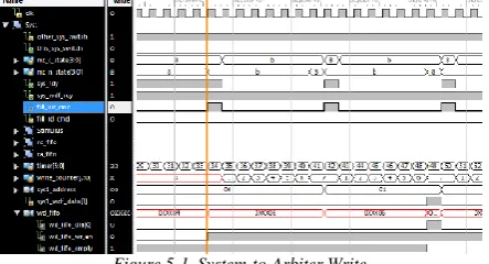
Fig. 4-2. System-to-Arbiter Write state diagram[2].
A. System-to-Arbiter Write
notifies the system that it has permission to communicate with the memory (through the arbiter). When the system first enters S8 the system can either send write commands or read requests to the arbiter. [14]
To send a write request, the system must assert the fill_wr_cmd, after having set starting address and the first 64-bits of data on their respective busses. Then, for the following seven clock cycles, the arbiter enters state S11 where the system must send the remaining 448 bits of data, 64 bits at a time. During these 7 clock cycles the arbiter will pick-up whatever is on the data bus and use it to fill the wd_fifo. During state S11, the system no longer has permission to send any new commands, and this will be evident by the de-asserted sys_rdy signal. Once the system finishes writing a full 512 bit data burst, the arbiter’s state machine returns to state S8, where it awaits for a new command from the system. To exit out of the S8-S11 loop, the system must be at S8 and one of the following events must happen: the systems sends a read request or arbiter_block timer expires. [15]
• Arbiter timer
The arbiter_block module contains a timer register which is used to keep track of how many clock cycles have elapsed since the system has been given permission to communicate with the arbiter. This is used to limit the number of clock cycles the system is given every time it has a turn.
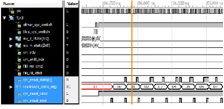
B. System-to-Arbiter Read-back
When the arbiter block first re-enters its System-to-Arbiter branch and finds that it has buffered data in its rd_fifo, it enters state 7. [16]During this state, 512 bit data packets are released from rd_fifo every 8 clock cycles. These 512 bit data packets are split up into a series of eight 64 bit packets which are then sent back to the system. Sys_read_data[0] shows the 0th bit of each one of these 64 bit data packets, while readback_data_reg shows eight bit representation of the 512 bit data packets as they are being released from the rd_fifo. These eight bits consist of every 64th bit in the 512 bit data packet. The read-back data that the system receives appears to match the write data the system sent, validating that the arbiter design works properly. However this is very limited validation of the design and is not enough to assure that it will work correctly when operating over millions of transactions.[13]
V. RESULTS
A. System-to-Arbiter Write
The arbiter was designed using Verilog, implemented using Xilinx Integrated Software Environment (ISE) .Figure 5-1, below, shows how at the 34th cycle in system-to-arbiter branch, Sys1 begins sending write commands. Fill_wr_cmd signal is asserted four times, once at the beginning of each new write command. The four writes are sent to addresses zero to three, as can be noted from looking at the sys1_address waveform. The data is sent 64 bits at a time, where every 0th bit in the 64 bits makes up 8 bit value corresponding to the address. This bit is apparent on the sys_wdf_data[0] signal which starts out equaling to a binary value of 00 at address zero , and binary 11 at address three. The stimulus module which sends these commands, attempts to send write data to addresses for address 0-31, but it is halted because the timer register reaches a value of 63, so the arbiter block must exist the branch, so Sys2’s arbiter block may enter it.
B. System-to-Arbiter Read-back
When the arbiter block first re-enters its System-to-Arbiter branch and finds that it has buffered data in its rd_fifo, it enters state 7. During this state, 512 bit data packets are released from rd_fifo every 8 clock cycles. These 512 bit data packets are split up into a series of eight 64 bit packets which are then sent back to the system. Sys_read_data[0] shows the 0th bit of each one of these 64 bit data packets, while readback_data_reg shows eight bit representation of the 512 bit data packets as they are being released from the rd_fifo. These eight bits consist of every 64th bit in the 512 bit data packet. The read-back data that the system receives appears to match the write data the system sent, validating that the arbiter design works properly. However this is very limited validation of the design and is not enough to assure that it will work correctly when operating over millions of transactions. Figure 5-2, below, shows how the system working with syste-to-arbiter read back.
Figure 5-2, system-to-arbiter read back.
VI. CONCLUSION
In this paper I have taken a close look at microarchitecture. I have given an overview of the major improvements to the architecture multi-core architectures with a special focus on the memory organization and cache coherency scheme. I have looked into several studies that have shown by state diagram and the effectiveness of these improvements. The inclusive,shared L3 cache has reduced much of the complexity and overhead associated with keeping caches coherent between cores. The integrated memory controller reduces memory access latencies. I have shown that the architecture scales well; it allows for as many cores as are needed for a particular application. Previous and competing architectures do not scale nearly as well; more cores can be added, but the limitations of the memory organization introduce bottlenecks to data movement. This position architecture well to be a flexible solution to future parallel processing needs.
ACKNOWLEDGMENT
Our thanks to the experts of KCG College Of Technology- Chennai. Dr. V. Ranganathan, Dr. M. Ramarathinam, Dr. V.Vidya devi and Mr. T. Thomas leonid who have contributed towards development of my project work.
REFERENCES
[1] Pablo Prieto, Valentin Puente, José-Ángel Gregorio “Multilevel Cache Modeling for Chip-Multiprocessor Systems” IEEE computer architecture letters, vol. 10, no. 2, july-december 2011.
[2] Prabhakar J., Senthilkumar M., Priya M.S., Mahalakshmi K., Sehgal P.K., Sukumaran V.G., "Evaluation of Antimicrobial Efficacy of Herbal Alternatives (Triphala and Green Tea Polyphenols), MTAD, and 5% Sodium Hypochlorite against Enterococcus faecalis Biofilm Formed on Tooth Substrate: An In Vitro Study", Journal of Endodontics, ISSN : 0099-2399, 36(1) (2010) pp. 83-86
[3] Muhammad Ali Ismail “Performance Behavior Analysis of the Present 3-Level Cache System for Multi-Core Systems using Queuing Modeling” International Conference on Latest Computational Technologies (ICLCT'2012) March 17-18, 2012 Bangkok
[4] Ramkumar Prabhu, M., Reji, V., Sivabalan, A., "Improved radiation and bandwidth of triangular and star patch antenna", Research Journal of Applied Sciences, Engineering and Technology, ISSN : 2040-7459, 4(12) (2012) pp. 1740-1748.
[5] S. K. Moore, “Multicore is bad news for supercomputers”, IEEE spectrum, 2008.
[7] C.K. Chow. “On Optimization of Storage Hierarchies”, IBM Journal of R&D, vol. 18, pp. 194-204, 1974.
[8] Saravanan, T., Saritha, G., "Buck converter with a variable number of predictive current distributing method", Indian Journal of Science and Technology, ISSN : 0974-6846, 6(S5) (2013) pp.4583-4588.
[9] D. Molka, D. Hackenberg, R. Schone, and M.S. Muller, “Memory Performance and Cache Coherency Effects on an Intel Nehalem Multiprocessor
System”, in 2009 18th International Conference on Parallel Architecturesand Compilation Techniques, September 2009
[10] Saravanan, T., Srinivasan, V., Sandiya, V.P., "A two stage DC-DC converter with isolation for renewable energy applications", Indian Journal of Science and Technology, ISSN : 0974-6846, 6(S6) (2013) pp. 4824-4830.
[11] JJ. Treibig, G. Hager, and G. Wellein, “Multi-core architectures: Complexities of performance prediction and the impact of cache topology”, Regionales Rechenzentrum Erlangen, Friedrich-Alexander Universiat Erlangen-urnberg, Erlangen, Germany, October2009
[11] V. Cuppu, B. Davis, B. Jacob and T. Mudge, "High-Performance DRAMs in Workstation Environments," IEEE Transactions on Computers, vol. 50, no. 11, pp. 1133-1153, 2001.
[12] Elpida Memory, Inc., "New Features of DDR3 SDRAM," March 2009.
[13] A. Hartstein, V. Srinivasan, T.R. Puzak, P.G. Emma. “On the Nature of Cache Miss Behavior: Is It SQRT(2)?”, Journal of Instruction-Level Parallelism 10, pp. 1-22, 2008.
[14] C. Kim, D. Burguer and S.W. Keckler. “Nonuniform Cache Architecture for Wire-delay dominated on-chip caches”, IEEE Micro, vol. 23, no. 6, pp. 99-107, 2003.
[15] N. Muralimanohar, R. Balasubramonian, N. P. Jouppi, ”Architecting Efficient Interconnects for Large Caches with CACTI 6.0.IEEE Micro vol. 28 No, pp. 69-79, 2008.
[16] Hewlett-Packard Development Company, LP., "Memory technology evolution: an overview of system memory technologies," December 2010. [17] TVUK Kumar, B Karthik, EB Kumaran, Visual Secret Sharing Scheme for JPEG Compressed Images, Middle-East Journal of Scientific Research 12 (12), PP 1873-1880, 2012.
[18] B Karthik, TVUK Kumar, EMI Developed Test Methodologies for Short Duration Noises, Indian Journal of Science and Technology 6 (5S), PP 4615-4619, 2013.
[19] Mr.B.Karthik, Dr.T.V.U. Kiran Kumar, N. Gomathi, Immobilizer Implementation using Mutual Authentication with enhanced security using 802.15.4 protocol,International Journal of Advanced Research in Electrical, Electronics and Instrumentation Engineering ,ISSN 2278 - 8875, pp 142-151, Vol. 1, Issue 3, September 2012.
[20] M.Jasmin,Bus Matrix Synthesis Based On Steiner Graphs For Power Efficient System On Chip Communications ,International Journal of Advanced Research in Electrical, Electronics and Instrumentation Engineering, ISSN 2278 - 8875 , pp 98-104,Vol. 1, Issue 2, August 2012. [21] M. Jasmin, A Low Power Pipelined FFT/IFFT Processor for OFDM Applications,International Journal of Advanced Research in Electrical, Electronics and Instrumentation Engineering,ISSN (Print) : 2320 – 3765, pp 4712-4721, Vol. 2, Issue 10, October 2013.
[22] M Jasmin, Low Power Design of the Processer Based on Architecture Modifications,International Journal of Advanced Research in Electrical, Electronics and Instrumentation Engineering,ISSN: 2278 – 8875, pp 2922-2927, Vol. 2, Issue 7, July 2013.
![Fig. 2-1. Eight-core Processor cache hierarchy[1]](https://thumb-us.123doks.com/thumbv2/123dok_us/7790190.1290472/2.595.187.409.139.326/fig-core-processor-cache-hierarchy.webp)
![Fig. 4-2. System-to-Arbiter Write state diagram[2].](https://thumb-us.123doks.com/thumbv2/123dok_us/7790190.1290472/4.595.198.400.369.705/fig-system-to-arbiter-write-state-diagram.webp)