5821
Power Control And Inter Symbol Interference Of
Optical – Wireless Link At Chip Level
Eethamakula Kosalendra, Dr.A.Bhavani SankarAbstract: The optical communication has developed as a practical solution to a high-speed transmission systems owing to the higher bandwidth of its encompassing greater data rates. With this study, the performance analysis of simple correlator as well as chip level detector in OCDMA- optical code division multiple access wireless systems for uplink is actually suggested. We check out the overall performance in 2 various situations of (ISI) being negligible and also the ISI degrading the receiver efficiency. Use of advanced modulation formats which could support higher data rates with easier spreader and receiver designs is actually among the appealing resolution to develop the spectrally effective high velocity optical transmission links. This particular method additionally motivates the scientists as well as style engineers to further examine the skills of various modulation platforms.
Keywords: Optical Wireless Communication, Optical orthogonal codes, RF technologies, Wireless link
————————————————————
1.
INTRODUCTION
Optical Wireless Communication (OWC) is actually viewed as probably the most significant technology of the evolution of broadband access systems. The very last 30 years have witnessed its considerable growth because of to which in a brief time span, OWC has turned into a complement for Radio Frequency (RF) technologies. Wireless technology demands a substitute broadband connection for web as well as multimedia products with good speed information transmission that could run in both long routines (outdoor program and hybrid interfaces) as well as for short haul (personal and indoor area network) connectivity [two - four]. For contemporary world, there's a higher dependency on large deployment of RF equipment as well as systems for both wireless and wire line communications. Nevertheless, utilization of RF band in Electromagnetic (EM) spectrum shows the limitation of its as a result of limited channel capability as well as high-priced licensing. Hence, actually - developing and unstoppable need for bandwidth need to find out different practical solutions running at top areas of EM spectrum. OWC incorporates special characteristics, as the link architecture of its resembles with point to point as well as point to multipoint Optical Fiber Communication (OFC) while not including the fiber wires. Additionally, qualities of OWC are actually much like RF systems with the exception this radio signals are now being swapped by light wave connected by specifically created antennas, optical trans receivers as well as printer driver circuits. Terrestrial FSO for broadband access communication is actually an obvious Line of Sight (LOS) method. Establishment of FSO link usually requires laser beam supply pointed as optical beam running in the range from 850 nm to 1550 nm with the atmospheric channel in order to link wireless communication for offering high - pace information transmission with bigger bandwidth. Unlike RF systems which employ omnidirectional transmission of signals as well as radiate energy in all of directions, FSO trans - receivers use narrow and directional highly beam, located at above the ground level or perhaps at the roof of developing for LOS propagation. It's inherent low likelihood of interception and also anti - jamming attributes as a result of the usage of narrow cone shaped laser beam.
Detection of power loss at receiver could be calculated very easily by virtue of LOS. Additionally, it's the potential to intercept optical beam, making it probably the safest phenomenon among pre-existing methods for large area connectivity. Rural areas which have geographically demanding surfaces in which broadband connectivity is quite tough via optical fiber link, FSO installation gets to be more feasible with lower maintenance cost. Due to advance optoelectronic components and laser diode, terrestrial FSO emerges as an efficient technique showing its significance as a reliable, stable and fully capable alternative to overcome several challenges like license free operation, multipath fading, inter-channel interference, health hazards caused by RF radiation, fiber maintenance, EM interference etc. Classifications of optical – wireless communication systems
OWC is now a trending area among industrial developers as well as investigation groups to look for maximum remedies with good - end results. A distinction of large diversity in OWC is actually based upon actual physical link as well as operating range configuration to refer to a variety of existing technologies situated in it. Largely, transmission range decides a great range of applications, based on which it could be classified into 5 divisions:
(a) Ultra short range OWC: It demands multichip with strongly packed packages or bundles e.g. chip - to - chip communication in processor for stack communication under electronics systems.
(b) Short range OWC: Integrating as well as designing designs of OWC effectively perform signal transmission for only water applications in which RF waves forget to transport info but light wave favorably transmit information. A few WPAN (Wireless Body and wpan) Area Networks (WBAN), VLC systems as well as Li - Fi links will also be operating within this particular division.
(c) Medium range OWC: It consists of the designs created for inter vehicular systems on highway and vehicular to establishing connectivity with wireless IR communication. For indoor applications, indoor IR along with VLC are essential areas of WLAN. (d) Long range OWC: Building to building connectivity
as inter and intra carriers are actually coming in this particular division.
(e) Ultra very long range OWC: Deep space backlinks as well as inter satellite connectivity for
____________________
Eethamakula Kosalendra Research Scholar, Dept. of ECE, Sri SatyaSai University of Technology & Medical Sciences, Sehore, Bhopal-Indore Road, Madhya Pradesh, India
transmission of information ranges in many a huge number of kilometers.
OCDMA SYSTEM DESCRIPTION
In OCDMA systems both operator communicates its corresponding data bits by its corresponding code. The
codes in optical systems may be constructed in different domains such as a combination, space, polarization,
wavelength, or time of them.
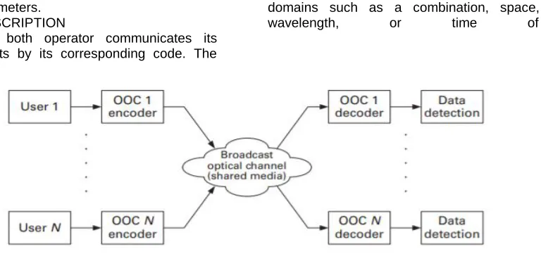
Figure 1 OCDMA general block diagram.
Because of specific conditions of wireless optical routes like scintillation as well as stage fluctuations, employing temporal codes in wireless OCDMA process in the context of immediate detection and intensity modulation is actually proven to be by far the most appealing. Hence from today on we think about wireless OCDMA systems with the pc user codes of theirs created on time domain. In these kinds of systems an information bit is actually mapped on a sequence of 0' and 1's in time url which constitute the corresponding code. The codes are intended like they're semi orthogonal. In this instance the correlation at the receiver side is able to distinguish information bits belonging to totally different users. We've found the common block diagram of an OCDMA process with N owners in Figure 1. For every user at the transmitter there's an encoder which creates the coded information stream. We believe OOC as the signature sequence in the system. Data stream of users are actually combined, added, i.e., in the shared media. At the receiver edge for every user there's a decoder which tries to regenerate the information share of the matching user with all the users' information bits.
Optical orthogonal codes
OOC are actually a family of (0,1) sequences with very good auto and cross correlation qualities providing asynchronous multiple contact infrastructures with cost-efficient functionality and basic synchronization of OCDMA communication networks. An OOC (L,w, λa, λc) is actually a family unit C of (zero, 1) sequences of length L with
continuous Hamming weight w satisfying the following 2 properties:
1. Auto-correlation property: for any code word x = (x0, x1, ..., xL−1) ∈ C, the inequality
holds for any integer τ 0 (mod L)
2. Cross-correlation property: for any two distinct code words x, y ∈ C, the inequality
holds for any integer τ, the place that the notation ⊕ denotes the modulo L addition. The tiny worth for λa as well as λc guarantees simple synchronization (of each transmitter–receiver pair) and also limited multiple access noise, respectively. When λa = λc = λ, we denote the OOC by (L,w, λ) for straightforwardness. The amount of code words of a family is actually known as the dimensions of the OOC. Originating from a practical perspective, a code with size that is big is ideal. To locate the absolute best codes, we have to figure out an upper bound on the dimensions of an OOC family with the specified parameters. Let (L,w, λa, λc) function as the largest possible size of an (L,w, λa, λc)-OOC. It's simple to show that if w(w' one) > λa(L' one) then (L,w, λa, λc) = zero of course, if w2 > λcL next (L,w, λa, λc) ≤ one. Nevertheless, depending on the Johnson bound for constant weight error correcting codes, we've the following bound
where the notation denotes the integer floor function. Also, it is clear from the definition that (L,w, λa, λc) ≤ (L,w, λ) where λ = max { λa , λc }
Out of the mutual interference point of view, probably the most desired on?off signature sequences are actually OOCs with λc = 1. Nevertheless, when we take a look at the ca with a few of owners interacting on each other's OOCs λc = 1 isn't always the optimum situation. The primary cause being that there's a trade off involving the code mass, λc as well as w. Bigger λc provides much more
interference between owners but on the additional hand enables having bigger code mass which alone raises the coding gain hence decreasing the entire interference. Briefly, the amount of owners of the network, receiver system, and target bit error fee determine the maximum values of OOC parameters.
Correlator structure
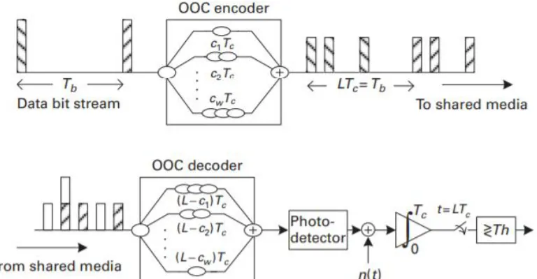
The easiest framework for an OCDMA receiver, specifically, correlator features a matched filter, corresponding to the code pattern of its, and also an incorporate as well as dump circuit. We've found the framework of a OCDMA transmitter such as encoder, as well as the correlator receiver of Figure 2. In this particular block diagram the decoder is actually matched to the corresponding code produced by the encoder. In fiber optic CDMA systems the matched filter could be applied by fiber tapped delay lines at the receiver side. Delay lines of each branch work to compensate for the corresponding delays induced at the encoder which constitute the corresponding OOC. The adequately delayed replicas add to put together the output correlator that is next given to the photo detector, dump, integrate, as well as thresholder electric circuit. In Figure 2 the white-colored
pulses at the feedback of the preferred decoder are actually the received signal from undesired users. The main benefit of the correlator system would be that the restricting high speed chip time decoding operation is actually done optically and passively. On the other hand in digital electric implementation, delays could be produced by employing flip flops. If we believe the sampling speed every chip identical to ns, nsL flip flops are actually adequate to put together the matched filter of the corresponding OOC code. If we denote the code length, the weight as well as the chip length by L, w, as well as Tc respectively, of course, if the roles of the pulsed mark chips corresponding to the code sequence is actually c1,c2,..., and cw, then the optical matched filter (passive optical tapped delay line) consists of w fiber delay lines each of which create a postpone equal to (L c1)Tc, (L
c2)Tc,... and,
Figure 2 OCDMA transmitter, and correlator receiver
(L − cw)Tc respectively. Considering only one bit duration, the output of the matched filter which is the combination of all w lines of the output signal has a peak at the time LTc if the transmitted bit is on. However, when the number of interfering users is equal to or greater than w, we may observe such a peak in the absence of the desired user‘s signal, i.e., the transmitted bit is off, and this causes an error.
Chip level AND logic gate
The conditional error probability provided the turbulence coefficient x could be evaluated not unlike the strategy utilized in indoor wireless OCDMA area. The conditional error probability provided the interference number, the interference pattern, as well as the fading coefficient is
actually received as follows,
where is the binary vector (detected after hard-limiter) caused on w marked chips, |n| is the hamming weight of
and are the chip level error probabilities on the jth chip for transmitting bit ‗0‘ and bit ‗1‘, while α and x are the known interference pattern and the
fading coefficient on that chip duration, respectively. Assuming the photoelectron counts in the jth chip to be
Gaussian, the error probabilities and c
are obtained as follows,
where TH is the ideal threshold for chip level detection and is obtained to minimize the total error probability. The total error probability is acquired by averaging the error
probability over the number of interfering
users l, the interfering pattern and the turbulence
coefficient x as follows,
where P (l, α), the probability to have l active interfering users with the intrusion design α, is obtained as follows,
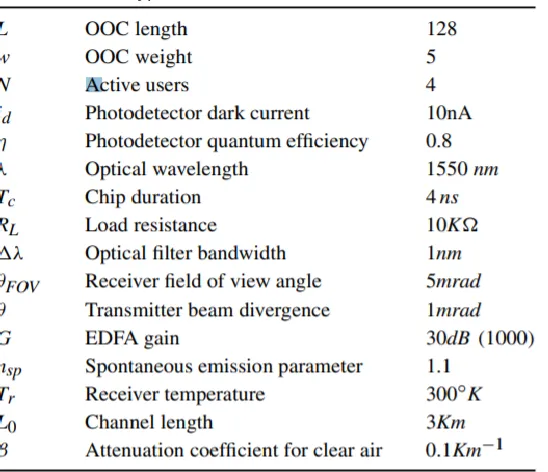
As an example, consider FSO link with restrictions listed in Table 1. Performances of the aforementioned receiver
structures are evaluated using the above represented expressions for the error probabilities.
Table 1 Typical values for the FSO OCDMA link.
The results of the digital component of the transmitter feed the analog element of the transmitter that has quick transistors as the driver before the LEDs operating in infrared wavelength (here 870 nm). To the receiver aspect we've used PIN photodiode following by a three stage amplifier circuit. The gains of the 3 stages are actually computed like they support the nominal parameters of the device.
CONCLUSION
Optical wireless communication is a pervasive and promising option for a lot of RF technologies. Optical Wireless systems are primarily categorized as indoor, outdoor, personal communication as well as hybrid OW / RF systems. This particular dissertation given several viable and unique methods associated with the deployment of indoor, hybrid and outdoor OW / RF systems for short too lengthy - range regimes. On one side for outside
applications, the commonly accredited FSO communication offers inherent benefits of supplying huge details speed with adaptable system schemes, making them an incredibly doable answer where other technologies face similar challenges. On the various other side, VLC systems have arisen as an excellent potential indoor OW technology that provide two performance as illumination and substantial - pace information transmission. Investigate contributions provided in this specific dissertation were concentrating on substantial theoretical analysis, experimental investigations and simulation studies to look at the link impairments occurred in outdoor and indoor OW systems
.
REFERENCES:
ranges up to 10°. These OPAs would allow data rates of 100Mbps at distances up to 0.5m.
[2] Acoleyen, Karel & Baets, Roel & Rogier, Hendrik. (2010). Chip-to-chip optical wireless link feasibility using optical phased arrays on silicon-on-insulator. 243 - 245. 10.1109/GROUP4.2010.5643367. [3] D. T. McGuiness, A. Marshall, S. Taylor, and S.
Giannoukos. 2018. Asymmetrical inter-symbol interference in macro-scale molecular communications. In Proceedings of the 5th ACM International Conference on Nanoscale Computing and Communication (NANOCOM '18). ACM, New York, NY, USA, Article 13, 6 pages. DOI: https://doi.org/10.1145/3233188.3233194
[4] Dasgupta, A., Mennemanteuil, M. M., Buret, M., Cazier, N., Colas-des-Francs, G., & Bouhelier, A. (2018). Optical wireless link between a nanoscale antenna and a transducing rectenna. Nature communications, 9(1), 1992. doi:10.1038/s41467-018-04382-7
[5] Kaushal, Hemani & Jain, Vk & Kar, Subrat. (2017). Overview of Wireless Optical Communication Systems. 10.1007/978-81-322-3691-7_1.
[6] Borah, D.K., Boucouvalas, A.C., Davis, C.C. et al. J Wireless Com Network (2012) 2012: 91. https://doi.org/10.1186/1687-1499-2012-91
[7] H. Safi, A. Dargahi and M. Matinfar, "Performance analysis of power control and inter-symbol interference for indoor optical wireless CDMA using chip-level detection," 2017 Iranian Conference on Electrical Engineering (ICEE), Tehran, 2017, pp. 1857-1862.
doi: 10.1109/IranianCEE.2017.7985356
[8] Jinous Shafiei Dehkordi, Gaetano Bellanca, and Velio Tralli. 2018. On-chip optical wireless interconnections with plasmonic nanoantennas: cross-link interference analysis. In Proceedings of
the 5th ACM International Conference on
Nanoscale Computing and
Communication (NANOCOM '18). ACM, New York, NY, USA, Article 36, 2 pages. DOI: https://doi.org/10.1145/3233188.3233221
[9] Wendemagegnehu T. Beyene and Amir Amirkhany (2008) ―Controlled Intersymbol Interference Design Techniques of Conventional Interconnect Systems for Data Rates Beyond 20 Gbps‖ IEEE TRANSACTIONS ON ADVANCED PACKAGING, VOL. 31, NO. 4, NOVEMBER 2008
[10] S. Khazraei M.R. Pakravan A. Aminzadeh-Gohari, ‖Analysis of power control for indoor optical wireless code-division multiple access networks using on–off keying and binary pulse position modulation‖ IET Commun., 2010, Vol. 4, Iss. 16, pp. 1919–1933
[11] Jazayerifar M., Salehi J.A.: ‗Atmospheric optical CDMA communication systems via optical orthogonal codes‘, IEEE Trans. Commun., 2006, 54, pp. 1614–1623
[12] El Badry, AA & El ghany, MA 2012, „CDMA Technique for Networkon-Chip‟,IEEE international symposium on design and diagnostics of electronics circuits and systems, pp.163-169. [13] El Badry, AA & El ghany, MA 2012, „CDMA
Technique for Networkon-Chip‟,IEEE international symposium on design and diagnostics of electronics circuits and systems, pp.163-169. [14] Ansari, MA, Song, J, Kim, M & Park, S 2009,
„Parallel test method for NoC-based SoCs‟ International SoC Design Conference (ISOCC), pp.116–119 .