IJSRR, 8(1) Jan. – Mar., 2019 Page 727
Research article Available online www.ijsrr.org
ISSN: 2279–0543
International Journal of Scientific Research and Reviews
Modeling and Mode Shape Extraction of Ball Grid Array Package on
Printed Circuit Board Soldered using Lead Free Solder Alloy –
SAC405
S Jayesh
1*and Elias Jacob
21
Department of Mechanical Engineering, School of Engineering, Cochin University of Science and Technology, Kochi, Kerala, India-682022
2
Department of Mechanical Engineering, School of Engineering, Cochin University of Science and Technology, Kochi, Kerala, India-682022,Email – [email protected],
ABSTRACT
Electronic apparatuses are wide-open to diverse vibration loadings. Vibration loading has become very substantial in the reliability valuation of contemporary electronic systems. The present challenge is to implement the vibration fatigue life examination quickly and precisely. Adding to that, lead is used as a solder joint in most of the electronics instruments. Lead is not eco-friendly due to its intrinsic nature of venomousness. A lead free solder joint is used in this paper which is 95.5Sn– 4.0Ag–0.5Cu (SAC405).Vibration analysis is conducted on a printed circuit board element (PCB) on which plastic ball grid array package (PBGA) of specific design is mounted which is our test specimen. The package is soldered to the PCB using Lead free solder material. The PCB which is used in the analysis is divided by drawing lines into elements having discrete points and excitation is given at those points while noting down the response. The PCB and the package along with the solder joint are modeled and modal analysis is done to find the natural frequency. Modal analysis experiment has been done and the finite element analysis results were validated. The mode shapes are extracted at the natural frequencies using DIAMOND software. Frequency Response Function (FRF) real and imaginary parts are obtained through LabVIEW software. The FRF data which are gained through the experiment are given as input to the DIAMOND software. Geometry, nodes, tracelines were also given as input. Then the mode shapes were extracted using the software.
KEYWORDS
:
lead-free, solder, material, mode shape, natural frequency*Corresponding author
Jayesh S
Department of Mechanical Engineering,
School of Engineering,
Cochin University of Science and Technology,
Kochi, Kerala, India-682022
IJSRR, 8(1) Jan. – Mar., 2019 Page 728
INTRODUCTION
The ball grid array (BGA) package has become a foremost packaging type in previous years,
because of its high capability for the input/output (I/O) counts. Connections mutually outside circuits
for these packages are normally through either the solder nuts or pins under the package. This result
would be reliability issues. Large number of solder ball and pin is present which is under high risk of
failure. This problem has attracted around attention from researchers directed toward the BGA
principle reliability in the soon years. Because of high quality of heat generated in such input-output
circuits, many researches were based on the thermal stress induced and the reliability related issues.
But when we consider the real world scenario, apart from these thermal stresses the components are
subjected to dynamic loading. For example consider the vibration loading a component is exposed
when it is transferred from one place to another. Real world applications related to automobiles,
ships, aircrafts and electronic equipment, vibration caused stresses are the dominant ones and it
cannot be neglected1.
The lead which which was in wide usage for soldering is not eco-friendly due to its inherent
toxicity. Electronic package industry is moving towards Pb-free solder in the past years because of
emerging environment regulations1. This affected the reliability aspect of the solder joint as no other alternative alloy was able to replace the lead-tin solder alloy. This results in the failure of IC
components in long run, which is a major impact on the electronics industry. From studies it was
made clear that solder were the most susceptible area of failure under the influence of dynamic
loading. Many of the electronic systems used in vibration atmosphere are exposed to random and
harmonic excitations2. Therefore, quality assurance of the electronic systems generally uses random vibration as the test specification requirement for acceptance, screening and reliability qualification
tests. First prototype is manufactured and after that the tests can be conducted. This is generally
feasible only after taking a long time, and is frequently seen as inefficient and not add to economy as
electronic technology markets nowadays are very fast developing. An electronic package is planned
and designed so as to protect an Integrated Circuit (IC) from chemical, mechanical, electrical, and
thermal harm. It should also provide interconnections to other devices. The integrated circuit is
becoming more complex. According to the Moore’s law: the transistor density of integrated circuit
will double in every 18 months. Functioning is becoming more difficult as a result of this. As an
example, Intel’s 4004 chip had 2,250 transistors in 1971 while Intel Itanium 2 Processor had 410
million transistors in 20033.
However, a large slice of research on high cycle fatigue is only regarding with predicting the
IJSRR, 8(1) Jan. – Mar., 2019 Page 729
vibration failure test, theoretical formulation for the calculation of the electronic component’s fatigue
life and FEA under sinusoidal vibration loading. Chen et al.5 applied vibration fatigue test and analysis procedure for flip chip solder joint fatigue life examination. Perkins and Sitaraman6 used linear sweep vibration analysis to illustrate the fatigue failure for ceramic column grid array
(CCGA). Da Yu et al.7 motivated on predicting the fatigue life of electronic components subjected to random vibration loading by adding both vibration tests and simulation analysis. Fang Liu et al.8 for examining the solder joint reliability of BGA packages under random vibration loading, vibration
reliability test of PCB assembly was done by using narrow-band random excitation. Yang et al.9 implemented the out-of-plane sweep sinusoidal vibration test to assess the reliability of the plastic
BGA (PBGA) assembly against vibration fatigue In the area of random vibration fatigue, Pitarresi et
al.10,11,12 considered the modeling techniques of circuit cards subjected to vibration loading. They investigated the response of surface mount lead/solder and predicted its fatigue life subjected to
random excitation. Zhou et al.13,14,15 matched the vibration reliability between the Sn-Pb and Pb-free solder joints under harmonic excitation and broad-band random vibration excitation. Some
researchers were devoted to investigating the life prediction model under random vibration16,17,18. Robin Alastair Amy et al.19 has done work to examine the accuracy of typical FE models used to predict the response of PCBs to harsh random vibration environment. It has been shown that if good
data on the board properties exists, then even simple PCB FE models can deliver very accurate
response prediction. Very less number of papers are there which deals with mode shape extraction of
the BGA mounted on PCB using lead free solder joints.
FINITE ELEMENT MODELING
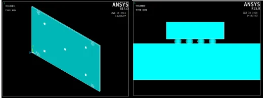
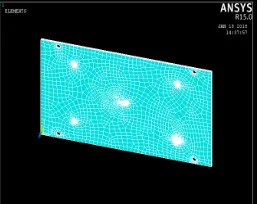
A finite element model of the PCB with ball grid arrays is modeled using commercial
software ANSYS 12.1. All components including the PCB was modeled by Solid element
(SOLID45). All the nodes at the location of screw holes were fixed in all degrees of freedom because
boundary conditions should represent those used in the vibration analysis. The image of the FEA
model of the same is shown in the figure 1. Material properties used are given in the table 1
IJSRR, 8(1) Jan. – Mar., 2019 Page 730 Figure 1 c) meshing of the model
Table 1: Material properties
Sl no. Materials
Young's modulus(Gpa)
Poisson's ratio
Density (Kg/m3)
1 PCB 25 0.28 3400
2 Solder ball(SAC405) 53.3 0.28 7440
3 Molding component 20 0.3 1890
EXPERIMENTAL SECTION
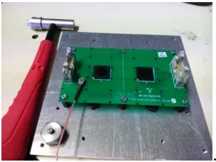
Two particularly designed BGA packages is mounted on the PCB. The BGA component, 19
x 19 mm, is mounted with 0.3 mm diameter lead-free solder balls with a pitch of 0.5 mm. The PCB
is made of FR4 material with length of 132 mm and width of 76 mm. It has a thickness of 1 mm.
Lead-free solder used for the experiment is 95.5Sn–4.0Ag–0.5Cu (SAC405) , the PCB assembly is
mounted on the vibration shaker machine and screwed at all the four corners. Dynamic signal
analyzer and accelerometer are used to note down the time history data of the shaker input as well
as the PCB response.
MODAL ANALYSIS
Two important parameters that describe the dynamic responses of test vehicle during
vibration analysis are Natural frequencies and mode shape. Experiments was performed for modal
analysis, also to determine the parameters, so that the FEA model can be validated. Figure 2 shows
the analysis set-up which is made arranged for the modal analysis. The grids were marked on the
board and the one of grid point is attached with accelerometer.All points were given excitation using
an impact hammer with random input. The accelerometer and impact hammer used for the analysis
IJSRR, 8(1) Jan. – Mar., 2019 Page 731
.
Figure2 Test set up of modal analysis
Table 2: Comparison of FEA results and experimental results
Sl no. Experimental Results(Hz) FEA Results(Hz)
1 161 151.76
2 310 300.25
3 411 423.37
4 579 585
MODE SHAPE EXTRACTION
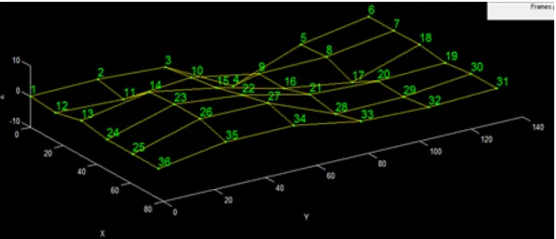
A mode shape expresses the deflection pattern associated with a certain modal frequency.
The PCB is divided into elements having discrete points and excitation is given at those points while
measuring the response. The response is measured at a point where the possibility for nodal point to
occur is minimum. FRF real and imaginary parts are obtained through LabVIEW software. The FRF
obtained by measuring the response at point i and an excitation at point j is equal to the FRF obtained
by measuring the response at point j and an excitation at point i. Measuring the response for impacts
at discrete points means that it captures the displacement at those discrete points so we can find a
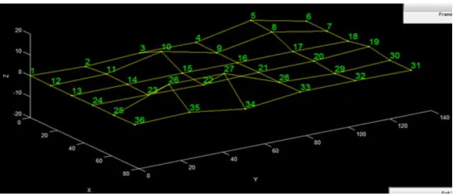
better picture of the deflection pattern at which it vibrates. Figure 3 shows the PCB divided into
elements.
IJSRR, 8(1) Jan. – Mar., 2019 Page 732
The PCB is divided into elements having 36 points and the excitation is given individually at
those points measuring the response with the accelerometer position fixed. FRF is computed for all
the 36 points.
DIAMOND (Damage Identification and Modal analysis for Dummies) is a new suite of
graphical-interface software algorithms to numerically simulate vibration analysis and to apply
various modal analysis, damage identification, and finite element model refinement techniques to
measured or simulated modal vibration data. DIAMOND has been developed at Los Alamos
National Laboratory. DIAMOND is written in MATLAB, a numerical matrix math application
which is available on all major computer platforms. DIAMOND is unique in three primary ways:
First is DIAMOND contains several of the most widely used modal curve-fitting algorithms.
Thus the user may analyze the data using more than one technique and compare the results directly.
This modal identification capability is coupled with a numerical test-simulation capability that allows
the user to directly explore the effects of various test conditions on the identified modal parameters.
Second is the damage identification and finite element model refinement modules are graphically
interactive, so the operation is intuitive and the results are displayed visually as well as numerically.
This feature allows the user to easily interpret the results in terms of structural damage.
Third one is DIAMOND has statistical analysis capability built into all three major analysis
modules: modal analysis, damage identification, and finite element model refinement. The statistical
analysis capability allows the user to determine the magnitude of the uncertainties associated with
the results20.
No other software package for modal analysis or damage identification has this capability.
The development of DIAMOND was motivated primarily by the lack of graphical implementation of
modern damage identification and finite element model refinement algorithms. Also, the desire to
have a variety of modal curve fitting techniques available and the capability to generate numerical
data with which to compare the results of each technique was a motivating factor. The authors are
unaware of any commercial software package that integrates all of these features. The FRF data
which are obtained through the experiment are given as input to the DIAMOND software. Geometry,
nodes, trace lines were also given as input. The geometry of the PCB defined is shown in the figure
IJSRR, 8(1) Jan. – Mar., 2019 Page 733 Figure 4 The geometry of the PCB defined in DIAMOND software
Figure 5 First mode shape at 161 Hz
Figure 6 Second mode shape at 306 Hz
IJSRR, 8(1) Jan. – Mar., 2019 Page 734 Figure 8 Fourth mode shape at 573 Hz
Figure 9 Fifth mode shape at 628 Hz
CONCLUSION
The specially designed Ball Grid Array Package soldered on PCB is modeled in ANSYS
software and the modal analysis was conducted to extract the natural frequencies. Experimental
modal analysis was conducted and the results of the finite element based modal analysis were
validated. The experimental results were matching with modal analysis done by the software. The
mode shapes at these natural frequencies were extracted using DIAMOND software.
REFERENCES
1. Chen YS et al. Combining vibration test with finite element analysis for the fatigue life
estimation of PBGA components. Micro electron Reliab 2008;48:638–44.
2. Introduction. In: Solder Joint Reliability Prediction for Multiple Environments. Springer,
Boston, MA,2009
3. Andrew E. Perkins - Suresh K. Sitaraman Solder Joint Reliability Prediction for Multiple
Environments, , springer
4. Sternberg DS. Vibration analysis for electronic equipment. 2nd ed. New York: John Wiley &
IJSRR, 8(1) Jan. – Mar., 2019 Page 735
5. Che FX, Pang John HL. Vibration reliability test and finite element analysis for flip chip
solder joints. Microelectron Reliab 2009;49:754–60.
6. Perkins A, Sitaraman SK. Vibration-induced solder joint fatigue failure of a ceramic column
grid array (CCGA) package. In: Proc 54th electronic components and technology conference,
Las Vegas; June 2004.
7. Da Yua et al. High-cycle fatigue life prediction for Pb-free BGA under random vibration
loading. Microelectronics Reliability 2011; 51: 649–656
8. Fang Liua, Guang Meng . Random vibration reliability of BGA lead-free solder joint.
Microelectronics Reliability 2013
9. Yang QJ, Wang ZP, Lim GH, et al. Reliability of PBGA assemblies under out-of-plane
vibration excitations. IEEE Trans Compon Pack Technol 2002;25(2):293–300
10.Pitarresi JM. Modeling of printed circuit cards subject to vibration. In: IEEE proceedings of
the circuits and systems conference, New Orleans, LA; May 3–5, 1990; 2104–7.
11.Pitarresi JM et al. The smeared properties approach to FE vibration modeling of printed
circuit cards. ASME J Electron Pack 1991;113(September):250–7.
12.Pitarresi JM, Akanda A. Random vibration response of a surface mounted lead/ solder joint.
In: Proc ASME international electronics packaging conference, Binghamton, NY; September
1993; 1: 207–17.
13.Zhou Y, Bassyiouni MA, Dasgupta. Vibration durability assessment of Sn3.0Ag0.5Cu and
Sn37Pb solder joints under harmonic excitation. ASME Trans J Electron Pack
2009;131(1):011016.
14.Zhou Y, Plaza G, Osterman M, Dasgupta A. Vibration durability of SnAgCu (SAC) solder
interconnects: random & harmonic excitation. J IEST 2009;52(1):63–86.
15.Zhou Y, Al-Bassyiouni M, Dasgupta A. Harmonic and random vibration durability of
SAC305 and Sn37Pb solder alloys. IEEE Trans Compon Pack Technol 2010;33(2):319–28
16.Yu D, Al-Yafawi A, Nguyen TT, Park S, Chung S. High-cycle fatigue life prediction for
Pb-free BGA under random vibration loading. Microelectron Reliab 2011;51:649–58
17.Han CW, Oh CM, Hong WS. Life prediction model development of BGA solder joint under
random vibration. In: ASME IMECE, Denver, Colorado; 2011; 987–8.
18.Yang P, Chen ZX. Experimental approach and evaluation on dynamic reliability of PBGA
assembly. IEEE Trans Electron Dev 2009;56(10):2243–9.
19.Robin Alastair Amy et al. Accuracy of simplified printed circuit board finite element models.
IJSRR, 8(1) Jan. – Mar., 2019 Page 736
20.Development of a General Purpose Code to Couple Experimental Modal Analysis and
Damage Identification Algorithms, Scott W. Doeblingl, Charles R. Farrar’, Phillip J.