GSJ: Volume 7, Issue 10, October 2019, Online: ISSN 2320-9186
www.globalscientificjournal.com
T
HEORETICAL
E
XPRESSION OF
F
ORBIDDEN
E
NERGY
L
EVEL AND
E
XIST-ENCE OF
T
INY
S
EGMENT
P
HOTON
.
Saddam Husain Dhobi
1, MD Jahangeer Rangrej
2, Pintu Verma
2, Mukesh Chaudhary
2,Rajhansh
Tiwari
21Author: Saddam Husain Dhobi is currently pursuing masters degree program in Physics in Tribhuvan University, Kathmandu, Nepal. E-mail: [email protected]
2Co-Author: MD Jahangeer Rangrej, Pintu Verma, Mukesh Chaudhary, and Rajhansh Tiwari is currently pursuing masters degree program in Physics in Tribhuvan
University, Kathmandu-44600, Nepal. Corrsponding E-mail: [email protected] , [email protected] , [email protected] , [email protected]
KeyWords
Tiny Segment Photon, Low Energy Photon, Kick Out, Energy level between Conductance and Valance band etc.
ABSTRACT
INTRODUCTION
In semiconductors, the Fermi level lies between the conduction and valence bands as shown in figure 1 below. When doping con-centration is increased, concon-centration of electrons in conduction band increase and pushes Fermi level higher in energy.
Figure 1: Location of Fermi energy level.
In the case of a degenerate semiconductor, an electron from the top of the valence band can only be excited into conduc-tion band above the Fermi level, since all the states below the Fermi level are occupied states [1].
Valence band: The range of energies possessed by valence electrons is known as valence band. The electrons in the outermost orbit
of an atom are known as valence electrons. In a normal atom, valence band has the electrons of highest energy and band may be completely or partially filled.
Conduction band: The range of energies possessed by conduction band electrons is known as conduction band. All electrons in the
conduction band are free electrons. If a substance has empty conduction band, it means current conduction is not possible in that substance.
Forbidden energy gap: The separation between conduction band and valence band on the energy level diagram is known as
forbid-den energy gap. No electron of a solid can stay in a forbidforbid-den energy gap as there is no allowed energy state in this region. The greater the energy gap, more tightly the valence electrons are bound to the nucleus.
Figure 2: Energy band at 0K tempera-ture.
Difference in energy levels between EC and EV is EG is show in figure 2 and for silicon is 1.12eV [2]. Multi-band gap materials offer
Figure 3: Presence of band in between Valance and conduction Band.
In IB materials, an electron is promoted from the VB to the CB through the IB. Upon absorption of sub-band gap-energy photons, the electrons transit from VB to CB and later from IB to CB. It will add up to the transition of electrons from VB to CB through conven-tional VB-to-CB photon absorption [3].
In order for conduction, shifting of electron distribution, more electrons has positive momentum than negative. The most negative values of p occupied in the ground state and shift them to positive values of p above pF. In terms of energy, shift some electrons to
energies above the Fermi level. To shift electrons above the Fermi level, there have to be available states near this level. The states very near the Fermi level, the material will have metallic conductivity [4]. It is seen that the Conduction band and Valence Band edg-es at all k points exhibit the same parity, introducing parity-forbidden transitions between band edgedg-es, consistent with the calculated zero transition matrix amplitudes. Such parity-forbidden transitions at all k points will lead to very poor optical absorptions of pho-tons with energies close to the bandgap values, consistent with the calculated optical absorption coefficients. The parity-forbidden transitions only affect the absorption coefficient [5].
Review
The difference in the selection rules for excitation of electronic energy levels of atoms and molecules by photons and by electrons. Practically all electronic transitions are allowed when low-energy electrons are used. They include transitions which are spin-forbidden and/or symmetry-spin-forbidden when photons are used. The transition energies above 11 eV, which are difficult to deal with optically, can be easily studied with electron-impact techniques. Lassettre and his students measure the of differential scattering cross-sections in several atoms and molecules using energy of electrons in between 400 and 600 eV and does not see such transi-tions. However, Schulz has used a low-energy electron (about 0.3 eV) impact method for determining electronic transitions in H2 and
H20 and observation of optically forbidden transitions [6].
When two semiconductors are joined, it is not clear in advance how the different bands in the two materials will line up in energy with one another, and their is no accurate predictive theory in practice. The Hetero-structure material system in which both elec-trons and holes see higher energies such system is called Type I system. Hetero-structures in which elecelec-trons and holes have their lowest energies such system is called Type II [7]. Keldysh confine to an analysis of the effects connected with the interactions be-tween the valence and conduction bands at a specified potential, particularly a Coulomb potential, with effective charge Ze, taking into account both the charge of the center and the effective dielectric constant. All the electronic levels lie in the upper half of the forbidden band. This rule is violated, if the deviations of the field from a Coulomb one are taken into account. The resonant capture of electrons at excited levels with subsequent cascade transition into the ground state [8].
The nuclear motion is negligible during the time required for an electronic excitation. Since the nuclei do not move during the ex-citation, the internuclear distances remain constant. The most probable component of an electronic transition involves only the ver-tical transitions. The electronic transition involves promotion of electron from a electronic ground state to higher energy state, usual-ly from a molecular orbital [9].
higher-order processes where electrons flip their spin. They find that the relaxation time is about 200 ms for forbidden transitions, 4 to 5 orders of magnitude longer than for allowed transitions. The transition from the spin-triplet state to the spin-singlet state is bidden by conservation of the total spin for both atomic helium and artificial helium. The difference between the allowed and for-bidden transitions leads to more than 11 orders of magnitude difference in the relaxation times for real hydrogen and helium atoms [10]. Although the atomic kinetics depend on, in particular, optical allowed transitions (E1), the weak forbidden transitions: magnetic dipole (M1) and electric quadrupole (E2) have been linked to dominant features in the optical spectra of planetary nebulae and the aurora. The lowest-order metastable levels radiatively decay correspond to M1 and E2 transitions. M1 and E2 transition rates are of several orders of magnitude smaller than those for E1 transitions with a similar energy level separation. Especially, forbidden transi-tions such as M1 and E2 are of great interest for plasma diagnostics and modeling [11].
Band spectrum is emitted by substances in the molecular state when the thermal excitement of the substance is not quite sufficient to break the molecules into continuous atoms. Franck-Condon Principle define as electronic transitions occur in a very short time and hence the atoms in a moleule do not have time to change position appreciably during electronic transition. The transitions occur from ground vibrational level of the ground electronic state to many different vibrational levels of particular excited electronic states [12]. Akram et al investigate quantum control and interference in a three level ladder system, which are extended to other schemes. They found high dependence and sensitivity on the relative phase of the pump and probe em modes of the relevant lasers. This sen-sitivity is particularly accentuated in the third transition, whose frequency is essentially the sum of the frequencies of the sequential transitions in the ladder, even when this transition is one photon emission forbidden in the bare state [13].
In the presence of two laser fields the initially dipole forbidden transition becomes dynamically permitted due to ac Stark effect which shown that such transitions exhibit quantum-interference-related phenomena, such as electromagnetically induced transpar-ency, gain without inversion and enhanced refractive index. The ladder configuration of a three level system interacting with two laser fields has been studied. Gennady et al. shown that strong coherence is established on the transition that originally was electric-dipole forbidden due to selection rules. However, the presence of two laser fields brakes the spherical symmetry and makes this transition dynamically allowed. They propose to use femtosecond comb for the pump and probe lasers where phase relation among components and such experiment looks for radiation at the forbidden transition frequency [14].
The investigation of the hyperfine interaction (HFI) of the spin of a magnetic ion with those nuclei for which the HFI is of the same order of magnitude as the Zeeman energy. The nuclear spin is quantized in an effective field which is the sum of the external field and the field due to the HFI. If the HFI and the Zeeman energy are of the same order, the direction of this effective field will change significantly during an electron spin transition. Hence the probability of a forbidden transition, in which the projection of the nuclear spin changes simultaneously with the electron spin projection and also be of the same order as the probability of an allowed transi-tion, in which only the electron spin projection changes [15].
Chemical and photochemical processes at semiconductor surfaces are highly influenced by the size of the band gap, and ability to control the band gap by particle size in nanomaterials is part of their promise. The combination of soft x-ray absorption and emission spectroscopies provides band-gap determination in bulk and nanoscale itinerant electron semiconductors such as CdS and ZnO, but not for all. The incident x-ray energy resolution was set to approximately 0.2 and 0.35 eV for absorption and emission spectroscopies, respectively. The x-ray emission spectrometer has a resolution of about 0.5 eV. The hematite band gap is more clearly discernable from measurements of photocurrent vs wavelength, and values of 2.14–2.2 eV for bulk samples are typical [16].
The valence band of [(In0.53Ga0.47)1-xMnx]As almost remains unchanged from that of the host semiconductor (In0.53Ga0.47)As, that
the Fermi level exists in the band gap and p-d exchange splitting in the valence band is negligibly small in (InGaMn)As. In the In0.87Mn0.13As sample, although the resonant peaks are very weak due to the large strain induced by the lattice mismatch between
InP and InMnAs show the Fermi level exists in the band gap and that the p-d exchange splitting in the valence band is negligibly small [17].
Many electrical, optical, and even some magnetic properties of crystals can be explained in terms of the band structure. If the Fermi energy is located in a band gap, the material is insulating or semiconducting otherwise metallic. Many-particle quantum physics tells us, that valid many-particle states can only be constructed, if one does not allow two electrons to occupy the same single particle level. The energy of the level filled with the last electron is called the Fermi energy EF. In order to determine EF, we need to count the
number of k-values, which is easy for a finite crystal. The first Brillouin zone contains as many k points as there are unit cells in a finite crystal. In most cases the energy bands are identical for both spin directions [18].
In order to kick out an electron at an energy of Eb below the Fermi surface to escape the material, the incident photon must have an
energy which exceeds Eb and the work function φ of the material. If hf > φ, then the emitted electrons will have a distribution of
being ejected is proportional to the density of occupied electronic. First some of the photon excited particles will scatter off phonons and electronic excitations within the material. Second, due to these secondary scattering processes, it is very unlikely that an elec-tron which is excited deep within the bulk, will ever escape from the material [19].
Those materials for which maximum of valence band and minimum of conduction band lie for same value of k is called direct bandgap materials and satisfies the condition of energy and momentum conservation (GaAs, InP, CdS). Those materials for which maximum of valence band and minimum of conduction band do not occur at same value of k is called indirect bandgap materials (Si and Ge) [20]. The absorption of photons takes place mainly at the band gap energy of each layer, and therefore, responses of layers of different bandgaps should be observed at different photon energies within the same spectral response curve. The absorption of photons at the bandgap energy generates electron-hole pairs, and the availability of photo-generated carriers gives rise to changes in various electrical properties. This configuration is commonly used in spectral photo-conductivity and in internal photoemission. The current flows perpendicular to a potential barrier formed between two materials, and only when the photon energy is great enough to excite electrons over the barrier, can an electric current be detected [21].
The absorption edge as reflected in the photo-current is affected mainly by the typically strong electric fields present at semiconduc-tor interfaces. The electric field assists photons with energy smaller than the bandgap to excite electrons across the forbidden gap by adding electric energy by electric field. The effect of electric fields on the absorption edge in semiconductors is commonly known as the Franz-Keldysh effect [22, 23].
The Coulomb interaction modifies significantly the optical properties due to the formation of correlated electron-hole pairs, and needs to be included. Initial efforts to add these excitonic effects, both numerically and semi-analytically, were made within the ef-fective mass approximation. Rees provided a more complete method to compare theory and experiment which including not only the electron-hole interaction but also lattice defects, band anisotropy, lifetime broadening and surface effects. He approach is the absorption spectrum without a dc field, which can then be convoluted with Airy functions that provide the field-induced effects [24]. If Zc open-shell electrons per unit cell and two spin states are available for each k-value then Zc may be odd and even. If even,
inte-gral number of bands is filled and the rest are empty ⇒ insulator. If odd then it is mandatory that at least one band is only partially filled ⇒ metal. In a metal with a nontrivial band structure, the concept of a Fermi surface is much less trivial than in the Sommerfeld model. For non-interacting, the lowest NZc states of the lowest band will be filled up to some energy EF = µ(0). A/c to Sommerfeld
model, µ(T) is not appreciably a function of T. It must have the symmetry of the crystal, but can be of a shape quite different from a sphere [25].
EF lies within the conduction band and E field is applied to a metal, electrons near EF can gain energy from E field and reach nearby
empty energy states. A lower or valence band is completely filled. The next higher electronic state in an atom is an energy gap Eg∼
10 eV higher and makes the conduction band. Eg >> kBT, and EF is about the midpoint of the gap. FD statistics says very few electrons
will reach the conduction band at T ∼ 300 K. Hence the material has a high resistivity [26].
METHODOLOGY
Let us consider an material is made up of an atom and he enrgy of the valence band is Ev and conduction band is Ec. The energy
dif-ference between them is called forbidden energy and gap is called forbidden gap. Since the energy gap between conduction and valence band implies the range of energy and goes to decrease when we move from valence to conduction band.
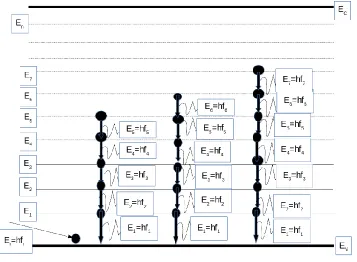
Let there is En level energy between them, on which electron excited when absorbed the energy from incidence photon, whose
en-ergy is less then the work function of an atom of consider material.
We have photoelectric equation
hfi=hf +K.E………...(1)
where hfi =incidence photon energy and fi is it correspond frequency.
where hf = work function of an atom of consider material and f is it correspond frequency.
Then from (1) we get,
hfi=hf ………...(2)
For consider material hf is fixed but hfi is not fixed i.e. we can incidence photon of variable energy but in our case we are
consider-ing those photon whose energy is less then hf.
Here hfi is the incidence energy observed by electron and goes to excitation state and emit same amount of energy, when come
back to ground state i.e. from different energy level existence in between conduction and valence band to valence band. But in this case the energy of emission photon from difference energy level to valence band is difference and the sum of total emission photon, when electron come from difference energy level existence between conduction and valance band to valance.
Then hfi=hf1+hf2+hf3 +hf4+………..+hfn + hff1+hff2+hff3+……+hffs………..(3)
Since E=hf then from (3)
Ei=E1+E2+E3 +E4+………..+En +Ef1+Ef2+Ef3 +………+Efs………..(4)
Where, E1 =energy level near valance band
E2 =another energy level next to E1
E3 =another energy level next to E2 and so on,
En = Energy level near to Fermi bottom level
Also here, Efs Fermi energy level included from bottom to top of its own
𝐸𝑖= ∑𝑛𝑙=1𝐸𝑙+ ∑𝑠𝑚=1𝐸𝑓𝑠………...(5)
This equation (5) show that the energy of incidence photon is divided into number of discrete packet in valance band conduction band and it is only possible, if a single incidence photon contain other photon inside it which may implies photon inside photon (Name tiny segment photon ). Tiny segment photon may play an important role during such transition of electron when energy of photon is less than work function of material.
In other hand, forbidden energy level in forbidden gap is possible because the attraction of the exciting electron with in the field of charge attraction by atom of the material is considerable. These attraction goes on decreasing as electron goes from valance to conduction band. Forbidden energy level is of fixed energy level but transition of electron from such energy level to valence energy level or valence is determine by the energy of incidence photon.
Due to the presence of these forbidden energy level in forbidden gap, the energy of single photon whose energy is less then work-function is divided into number of tiny segment photon. Since the energy of tiny segment photon is very very less and is emitted when electron transition take place in between forbidden gap and forbidden energy level. This tiny segment photon energy called the absorption energy of the material i.e. absorption of energy by material when energy of incidence photon is less than work func-tion of a material.
Let us considering a material and a photon incidence on it. Let hf is the work-function of a material which is greater than energy of incidence photon, then from equation (5), we take are considering three cases in term of incidence photon energy.
Case I:Energy of incidence photon is very less then work function: When energy of incidence photon Ei=hfi is very less then
work-function Φ=hf then in this case electron is not going to produce photo-electric current because the energy of incidence photon is very less. But the electron tends toward conduction band from valence band. Since energy carrying by electron is less, it goes on photo emission i.e. it come to valance band by emitting the photons of energies hfi.
In this case the number of energy level is less that mean number of emission photons is less then Case II and Case III because due to very less energy of incidence photon, consider electron contain less amount and travel the distance toward the conduction band from valance band is less, and hence electron goes to cross less energy level.
than Case II and III as shown in figure 4. Here we consider energy of incidence photon whose energy is very less than work function and given figure 4 is an example when incidence photon goes energy level which is very slight greater than valance band energy.
Figure 4 :
Ener-gy of incidence
photon in very less than
work function.
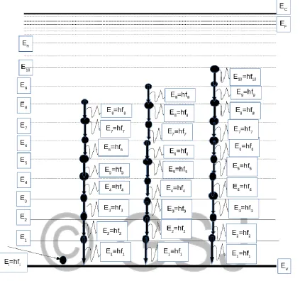
Case II: Energy of inci-dence
photon is medium less than work function: When energy of incidence photon Ei=hfi is medium less than work-function Φ=hf then
in this case also electron is not going to produce photo-electric current because the energy of incidence photon is medium less. But the electron tends toward conduction band from valence band. Since energy carrying by electron is less, it goes on photo emission i.e. it come to valance band by emitting the photons of energies hfi.
In this case the number of energy level cross by electron is less than Case III and grater than Case I that mean number of emission photons is less than Case III and greater than Case I because due to medium less energy of incidence photon, consider electron con-tain sightly more energy then Case I and travel the distance toward the conduction band from valance band is sightly more than Case I less, and hence electron goes to cross slightly more energy level than Case I and less energy level than Case III. The energy level and photon emission in this Case is shown in figure 5.
Figure 5 : Energy of incidence photon in medium less than work function.
Case III: Energy of incidence photon is slightly less than work function: When energy of incidence photon Ei=hfi is slightly then
work-function Φ=hf then in this case also electron is not going to produce photo-electric current because the energy of incidence photon is less. But the electron tends toward conduction band from valence band. Since energy carrying by electron is less, it goes on photo emission i.e. it come to valance band by emitting the photons of energies hfi.
In this case the number of energy level is greater, that mean number of emission photons is greater than Case I and Case I because due to energy of incidence photon greater than Case I and Case II, consider electron contain slightly more amount of energy and travel the distance toward the conduction band from valance band more, and hence electron goes to cross more energy level than Case I and Case II.
Figure 6 : Energy of incidence photon in slightly less than work function.
RESULT AND DISCUSSION
CONCLUSION
Hence, from above mathematical relation we can identify the presence of forbidden energy level in forbidden gap due to the result-ant potential or charge attraction on electron when electron take energy of incidence photon whose energy is less then work func-tion of material. On the other hand we can also identify the tiny segment photon produce when electron coming from upper forbid-den energy level to valence band and due to the presence or emission of tiny segment photon the energy of inciforbid-dence photon is ab-sorbed by material when energy of incidence photon is less than work function of a material.
Acknowledgment
We would like to thanks all the team member of Innovative Ghar Nepal and Hypersales Pvt Ltd to provide research space and peace-ful environment during our research work.
References
[1] P. Ravindran, PHY02E – Semiconductor Physics, Bandgap engineering: Department of Physics, Central University of Tamil Nadu, India, pp. 3-4, Autum 2013, 17 December.
[2] D. W. Graham, Overview of Silicon Semiconductor Device Physics, Lane Department of Computer Science and Electrical Engineering, West Virginia University, pp. 3-4, 2009. (presentation).
[3] M. Rasukkannu, D. Velauthapillai, and P. Vajeeston, Computational Modeling of Novel Bulk Materials for the Intermediate-Band Solar Cells, ACS Omega, 2, pp. 1454-1455, 2017. DOI: 10.1021/acsomega.6b00534.
[4] M. R. Roussel, Chemistry 2000 Lecture 7: Band Theory of Bonding in Crystalline Solids, pp. 9-10, January 17, 2019.
[5] W. Meng, X. Wang, Z. Xiao, J. Wang, D. B. Mitzi, and Y. Yan, Parity-Forbidden Transitions and Their Impacts on the Optical Absorption Properties of Lead-Free Metal Halide Perovskites and Double Perovskites , pp. 7- 22.
[6] A. Kuppermann and L. M. Raff, Electron-Impact Spectroscopy, pp. 30-31, 29th January, 1963. (Received).
[7] D. A. B. Miller, Optical Physics of Quantum Wells, AT&T Bell Laboratories Holmdel, NJ07733-3030, USA, Rm. 4B-401. [8] L. V. Keldysh, Soviet Physics: Journal of Experimental and Theoretical Physics, 18(1), pp. 253-258, January, 1964. [9] UV-Vis spectroscopy: Electronic Absorption Spectroscopy, pp. 4-6.
[10] T. Fujisawa, D. G. Austing, Y. Tokura, Y. Hirayama, and S. Tarucha, Allowed and Forbidden Transitions in Artificial Hydrogen and Helium Atoms, Letters to Nature, 419, pp. 278-280, 2002.
[11] L. Özdemir, S. Kabakç, and E. ArmaLan, Forbidden Transitions in the Ground State Configuration of Doubly Ionized Argon, Hindawi Publishing Corporation: Journal of Atomic and Molecular Physics, Volume 2014, pp. 1-4, 2014.
[12] [S. L. Reddy, T. Endo and G. S. Reddy, Advanced Aspects of Spectroscopy, Electronic (Absorption) Spectra of 3d Transition Metal Complexes: Chapter 1, INTECH, pp. 4-5, 2012.
[13] U. Akram, J. Evers, and C.H. Keitel, Multiphoton Quantum Interference on a Dipole-Forbidden Transition, Journal of Physics B: Atomic, Molecular and Optical Physics, 38(4):L69, 2005.
[14] G. A. Koganov, R. Shuker, Phase Sensitive Quantum Interference on Forbidden Transition in Ladder Scheme, Preprint Submitted to Elsevier, pp. 1-8, October 12, 2018.
[15] T. I. Sanadze and G. R. Khutsishvili, Forbidden Transitions and Discrete Saturation In Epr Lines. Ii, Soviet Physics:Journal of Experimental and Theoretical Phys-ics, 32(3), pp. 412, March, 1971.
[16] B. Gilbert, C. Frandsen, E. R. Maxey, and D. M. Sherman, Band-Gap Measurements of Bulk and Nanoscale Hematite by Soft X-ray Spectroscopy, Physical Review B, 79, pp. 1-4, 2009. DOI:10.1103/PhysRevB.79.035108
[18] A. Wacker, An Introduction to the Concept of Band Structure, Mathematical Physics, Lund University, pp.1-6, November 20, 2018. [19] Bloch & Slater, Chapter 7: The Electronic Band Structure of Solids, pp. 17-19, March 2, 2017.
[20] A. P. Vajpeyi, Analog & Digital Electronics, Course No: Ph-218 (Tutorial -1), Department Of Physics, Indian Institute of Technology Guwahati, India, pp. 2-3. [21] Y. Turkulets and I. Shalish, Probing Dynamic Behavior of Electric Fields and Band Diagrams in Complex Semiconductor Heterostructures, pp. 2-3, 17
Novem-ber, 2017.
[22] K. Seeger, Semiconductor Physics 9th Edn. Springer, Berlin, pp.340, 2004.
[23] N. B. Ashkenasy, L. Kronik, Y. Shapira, Y. Rosenwaks, M. C. Hanna, M. Leibovitch, P. Ram, Surface Photovoltage Spectroscopy of Quantum Wells and Super-lattices, Applied Physics Letter, 68, pp. 879, 1996. DOI: 10.1063/1.116217
[24] F. D. Gomez and J. E. Sipe, The Franz-Keldysh Effect Revisited: Electroabsorption Including Interband Coupling and Excitonic Effects, pp. 1-2, March 10, 2014. [25] A. J. Leggett, Lecture 4: Basic Elements of Band Theory, pp. 5-6, summer 2010.