e-ISSN: 2278-067X, p-ISSN: 2278-800X, www.ijerd.com
Volume 9, Issue 1 (November 2013), PP. 15-21
New Efficient Bridgeless Cuk Rectifiers for PFC Application on
d.c machine
Siriki.s.m.ravi kumar
1,
T. Srinivasa Rao
2, K.durga rao
3,
1P.G Student Scholar, M.Tech Associate Professor 2, M.Tech Assistant Professor3, 1,2,3
Department of Electrical & Electronics Engineering
1,2,3Avanthi Institute of Engineering & Technology, Makavarapalem(P),Vishakhapatnam(Dt), Andhra Pradesh, India.
Abstract:- Three new bridgeless single-phase ac–dc power factor correction (PFC) rectifiers based on Cuk topology are proposed. The proposed topologies are designed to work in discontinuous conduction mode (DCM) to achieve almost a unity power factor and low total harmonic distortion of the Input current. The DCM operation gives additional advantages such as zero-current turn-ON in the power switches, zero-current turn-OFF in the output diode, and simple control circuitry. proposed topology is worked on discrete d.c machine .To show the performance between resistance load and discrete d.c machine.
Index Terms:- Bridgeless rectifier, Cuk converter, low conduction losses, power factor correction (PFC), rectifier, single-ended primary-inductor converter (SEPIC) converter, total harmonic distortion (THD).
I. INTRODUCTION
POWER supplies with active power factor correction (PFC) techniques are becoming necessary for many types of electronic equipment to meet harmonic regulations and standards, such as the IEC 61000-3-2. Most of the PFC rectifiers utilize a boost converter at their front end. In an effort to maximize the power supply efficiency, considerable research efforts have been directed toward designing bridgeless PFC circuits, where the number of semiconductors generating losses is reduced by essentially eliminating the full bridge input diode rectifier. A bridgeless PFC rectifier allows the current to flow through a minimum number of switching devices compared to the conventional PFC rectifier. Accordingly, the converter conduction losses can be significantly reduced and higher efficiency can be obtained, as well as cost savings. Recently, several bridgeless PFC rectifiers have been introduced to improve the rectifier power density and/or reduce noise emissions via soft-switching techniques or coupled magnetic topologies [1]–[9]. the voltage. To overcome these drawbacks, several bridgeless topologies, which are suitable for step-up/step-down applications have been recently introduced in [10]–[13]. However, the proposed topology in [10] still suffers from having three semiconductors in the current conduction path during each switching cycle. In [11]–[23], a bridgeless PFC rectifier based on the single ended primary-inductance converter (SEPIC) topology is presented. Similar to the boost converter, the SEPIC converter has the disadvantage of discontinuous output current resulting in a relatively high output ripple. However, the input line current cannot follow the input voltage around the zero crossings of the input line voltage; besides, the output to input voltage ratio is limited to half. Also, buck PFC converter results in an increased total harmonic distortion (THD) and a reduced power factor [15]. The Cuk converter offers several advantages in PFC applications, such as easy implementation of transformer isolation, natural protection against inrush current occurring at start-up or
Overload current, lower input current ripple, and less electromagnetic interference (EMI) associated with the discontinuous conduction mode (DCM) topology [16], [17]. Unlike the SEPIC converter, the Cuk converter has both continuous input and output currents with a low current ripple. Thus, for applications, which require a low current rip ple at the input and output ports of the converter, the Cuk converter seems to be a potential candidate in the basic converter topologies
II. PROPOSED BRIDGELESS CUK PFC RECTIFIERS
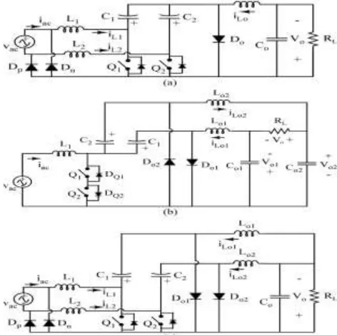
conventional Cuk rectifier. In addition, Fig. 1(a) and (c) shows that one rail of the output voltage bus is always connected to the input ac line through the slow-recovery diodes Dp and Dn or directly as in the case of the topology of Fig. 1(b). Thus, the proposed topologies do not suffer from the high common-mode EMI noise emission problem and have common-mode EMI performance similar to the conventional PFC topologies. Consequently, the proposed topologies appear to be promising candidates for commercial PFC products.
The proposed bridgeless rectifiers of Fig. 2 utilize two power switches (Q1 and Q2). However, the two power switches can be driven by the same control signal, which significantly simplifies the control circuitry. Compared to the conventional Cuk topology, the structure of the proposed topologies utilizes one additional inductor,
Fig.1. Proposed bridgeless Cuk PFC rectifiers. (a) Type 1. (b) Type 2. (c) Type 3.
Fig. 3. Equivalent circuits for type-3 rectifier. (a) During positive half-line period. (b) During negative half-line period of the input voltage.
This is often described as a disadvantage in terms of size and cost. However, a better thermal performance can be achieved with the two inductors compared to a single inductor. It should be mentioned here that the three inductors in the proposed topologies can be coupled on the same magnetic core allowing considerable size and cost reduction. Additionally, the “near zero-ripple-current” condition at the input or output port of the rectifier can be achieved without compromising performance
III. PRINCIPLE OF OPERATION
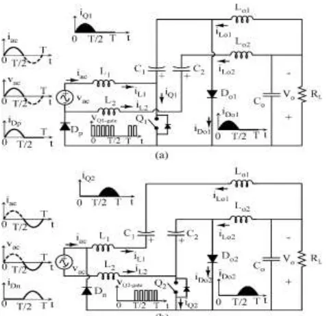
The proposed bridgeless type-1 Cuk rectifier of Fig. 1(a) will be considered in this study. Type 1 is similar to type 3, except for the output stage stresses. The SEPIC version of type 2 has been analyzed in [19]. The analysis assumes that the converter is operating at a steady state in addition to the following assumptions: pure sinusoidal input voltage, ideal lossless components, and all capacitors are large enough such that their switching voltage ripples are negligible during the switching period Ts .Moreover, the output filter capacitor Co (Co 1 and Co 2 for topology 2) has a large capacitance such that the voltage across it is constant over the entire line period. Referring to Fig. 2(a), during the positive half-line cycle, the first dc– dc Cuk circuit, L1–Q1–C1–Lo 1–Do , is active through diode Dp , which connects the input ac sourceto the output. During the negative half-line cycle, as shown in Fig. 2(b), the second dc–dc Cuk circuit, L2–Q2 -C2–Lo 2–Do, is active through diode Dn , which connects the input ac source to the output. As a result, the average voltage across capacitor C1during the line cycle can be expressed as follows:
distinct operating stages during one switching period Ts. Equivalent circuits over a switching period Ts in the positive half-line period of Fig. 2(a) The topological stages of type 1 over a switching cycle can be briefly described as follows.
Stage 1[t0, t1 ], : This stage starts when the switch Q1 is turned ON. Diode Dp is forward biased by the inductor current iL1. As a result, the diode Dn is reverse biased by the input voltage. The output diode Do is reverse biased by the reverse voltage (vac + Vo ), while Do is reverse biased by the output voltage Vo . In this stage, the currents through inductors L1 and Lo 1 increase linearly with the input voltage, while the current through Lo 2 is zero due to the constant voltage across C2. The inductor currents of L1 and Lo 1 during this stage are given by
Accordingly, the peak current through the active switch Q1 is given by
Where Vm is the peak amplitude of the input voltage v ac, D1 is the switch duty cycle, and Le is the parallel combination of inductors L1 and Lo 1 .
Stage 2[t1, t2]: This stage starts when the switch Q1 is turned OFF and the diode Do 1 is turned ON simultaneously providing a path for the inductor currents iL 1 and I Lo1 . The diode Dp remains conducting to provide a path for iL 1 . Diode Do remains reverse biased during this interval. This interval ends when iDo reaches zero and Do 1 becomes reverse biased. Note that the diode Do is switched OFF at zero current. Similarly, the inductor currents of L1 and Lo 1 during this stage can be represented as follows:
Stage 3[t2, t3 ]: During this interval, only the diode Dp conducts to provide a path for iL 1 . Accordingly, the inductors in this interval behave as constant current sources. Hence, the voltage across the three inductors is zero. The capacitor C1 is being charged by the inductor current iL 1 . This period ends when Q1 is turned ON. By applying inductor volt-second across L1 and Lo 1 , the normalized length of the second stage period can be expressed as follows:
IV. MATLAB MODELING AND SIMULATION RESULTS
Fig.4 Matlab/Simulink Model of Proposed efficient bridgeless rectifier with d.c machine
Fig.5 Output Voltage
Fig.6 Output Current
Fig 8 voltage of inductor l1&l2
Fig 9 voltage & current of inductor 3
V. CONCLUSION
Three single-phase ac–dc bridgeless rectifiers based on Cuk topology are presented and discussed in this paper. The validity and performance of the proposed topologies are verified by simulation and experimental results. Due to the lower conduction and switching losses, the proposed topologies can further improve the conversion efficiency when compared with the conventional Cuk PFC rectifier. Namely, to maintain the same efficiency, the proposed circuits can operate with a higher switching frequency. Thus, additional reduction in the size of the PFC inductor and EMI filter could be achieved. The proposed bridgeless topologies can improve the efficiency by approximately 1.4% compared to the conventional PFC Cuk rectifier. The performance of two types of the proposed topologies was verified on a 150Wexperimental prototype. The measured efficiency of the prototype rectifier at 100 Vrms line and full load is above 93% with THD below 2%. Experimental results are observed to be in good agreement with simulation results.
REFERENCES
[1]. W. Choi, J.Kwon, E. Kim, J. Lee, and B.Kwon, “Bridgeless boost rectifier with lowconduction losses and reduced diode reverse-recovery problems,” IEEE Trans. Ind. Electron., vol. 54, no. 2, pp. 769–780, Apr. 2007.
[2]. G. Moschopoulos and P. Kain, “A novel single-phase soft-switched rectifier with unity power factor and minimal component count,” IEEE Trans.Ind. Electron., vol. 51, no. 3, pp. 566–575, Jun. 2004.
[3]. R.-L. Lin and H.-M. Shih, “Piezoelectric transformer based current-source charge-pump power-factor-correction electronic ballast,” IEEE Trans.Power Electron., vol. 23, no. 3, pp. 1391–1400, May 2008.
[4]. S. Dwari and L. Parsa, “An efficient AC–DC step-up converter for lowvoltage energy harvesting,” IEEE Trans. Power Electron., vol. 25, no. 8, pp. 2188–2199, Aug. 2010.
[5]. Y. Jang and M. Jovanovic, “A bridgeless PFC boost rectifier with optimized magnetic utilization,” IEEE Trans. Power Electron., vol. 24, no. 1, pp. 85–93, Jan. 2009.
[6]. L. Huber, Y. Jang, and M. Jovanovic, “Performance evaluation of bridgeless PFC boost rectifiers,” IEEE Trans. Power Electron., vol. 23, no. 3, pp. 1381–1390, May 2008.
[7]. B. Su and Z. Lu, “An interleaved totem-pole boost bridgeless rectifier with reduced reverse-recovery problems for power factor correction,” IEEE Trans. Power Electron., vol. 25, no. 6, pp. 1406–1415, Jun. 2010.
[9]. H.-Y. Tsai, T.-H. Hsia, and D. Chen, “A family of zero-voltage-transition bridgeless power-factor-correction circuits with a zero-current-switching auxiliary switch,” IEEE Trans. Ind. Electron., vol. 58, no. 5, pp. 1848– 1855, May 2011.
[10]. W. Wei, L. Hongpeng, J. Shigong, and X. Dianguo, “A novel bridgeless buck-boost PFC converter,” in Proc. IEEE
Power Electron. Spec. Conf.,2008, pp. 1304–1308.
[11]. E. H. Ismail, “Bridgeless SEPIC rectifier with unity power factor and reduced conduction losses,” IEEE Trans. Ind. Electron., vol. 56, no. 4,pp. 1147–1157, Apr. 2009.
[12]. A. Sabzali, E. H. Ismail, M. Al-Saffar, and A. Fardoun, “New bridgeless DCM sepic and Cuk PFC rectifiers with low conduction and switchinglosses,” IEEE Trans. Ind. Appl., vol. 47, no. 2, pp. 873–881, Mar./Apr. 2011.
[13]. M. Mahdavi and H. Farzanehfard, “Bridgeless SEPIC PFC rectifier with reduced components and conduction losses,” IEEE Trans. Ind. Electron., vol. 58, no. 9, pp. 4153–4160, Sep. 2011.
[14]. M. R. Sahid, A. H. M. Yatim, and T. Taufik, “A new AC-DC converterusing bridgeless SEPIC,” in Proc. IEEE Annu. Conf. Ind. Electron. Soc., Nov. 2010, pp. 286–290.
[15]. J. M. Alonso, M. A. Dalla Costa, and C. Ordizl, “Integrated buck-flyback converter as a high-power-factor off-line power supply,” IEEE Trans. Ind.Electron., vol. 55, no. 3, pp. 1090–110, Mar. 2008.
[16]. M. Brkovic and S. Cuk, “Input current shaper using Cuk converter,” in Proc. Int. Telecommun. Energy Conf., 1992, pp. 532–539.
[17]. D. S. L. Simonetti, J. Sebastian, and J. Uceda, “The discontinuous conduction mode Sepic and Cuk power factor preregulators: Analysis and design,” IEEE Trans. Ind. Electron., vol. 44, no. 5, pp. 630–637, Oct.1997.