Effect of Annealing Temperature on Optical and
Electrical Properties of Electron Beam
Evaporated NiO Thin Films
A. Madhavi G. S. Harish
Research Scholar Research Scholar
Department of Physics Department of Physics
Sri Venkateswara University, Tirupati,517502, India Sri Venkateswara University, Tirupati,517502, India
P. Sreedhara Reddy Professor Department of Physics
Sri Venkateswara University, Tirupati,517502, India
Abstract
Nickel oxide (NiO) thin films were prepared by electron beam evaporation technique and studied various properties at different annealing temperatures. The surface morphology of the deposited films was characterized by scanning electron microscopy (SEM) and the compositional analysis of the deposited films was studied by energy dispersive spectroscopy (EDAX). The effect of the annealing process on the topography of the prepared NiO thin films was studied by atomic force microscope (AFM) at room temperature. The optical band gap of the as-deposited film was increased to 3.68 eV with the increase of annealing temperature up to 400oC, thereafter decreased at higher annealing temperature. Thin film samples annealed at 400oC showed decreased resistivity compared to other samples.
Keywords: atomic force microscopy, band gap, electron beam evaporation, NiO thin films, SEM, XRD
________________________________________________________________________________________________________
I. INTRODUCTION
Nickel oxide is a low cost material allowing for good cyclic reversibility, high coloration efficiency and good durability. NiO is a model for p-type metal oxide material which has very interesting characteristics such as good chemical stability and excellent electrical properties [1-5]. NiO films are commonly prepared by thermal evaporation, sputtering, spray pyrolysis, electrochemical deposition, sol- gel and electron beam evaporation techniques [6-10]. NiO thinfilms find very attractive applications on smart windows or displays to be used in automobiles, buildings or airplanes and are used in gas sensor applications because of the enhanced electrical properties. The properties of the deposited NiO films by electron beam evaporationtechnique, mainly depend on the deposition parameters such as substrate temperature, evaporation time, base pressure, working pressure, acceleration voltage and filament current. In this work, thin films of NiO have been deposited using electron beam evaporation technique and the effect of annealing temperature on the films has been investigated on structural, morphological, optical and electrical properties.
II. EXPERIMENTAL AND CHARACTERIZATION TECHNIQUES
Table – 1
The deposition parameters maintained during the preparation of NiO films
Parameters Values
The target to substrate distance 50 mm Base pressure 6.6 x 10⁻⁵ Pa Working pressure 2 x 10⁻⁴ Pa Substrate temperature 473 K
Evaporation time 10 min Accelerating voltage 5 kV
Filament current 120 mA
III. RESULTS AND DISCUSSION
Structural Analysis:
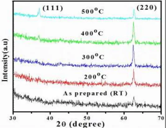
Thermal annealing is one of the most important factors, since annealing temperature can improve the crystal quality and reveal structural defects in thin films.During the annealing process, the structure and the stoichiometric ratio of the films change due to the movement of dislocations and defects.Fig.1 shows the X-ray diffraction patterns of NiO films annealed at different temperatures (30 0C, 200 0C, 300 0C, 400 0C and 500 0C). The crystallite orientation, lattice parameter and crystallite size as a function of annealing temperature is shown in table 2.
Fig. 1: X-ray diffraction patterns of NiO films deposited at different annealing temperatures
Table – 2
Crystallite size, Orientation and lattice parameter values of NiO thin films deposited at different annealing temperatures by Electron beam evaporation method
Sample (oC) Orientation Crystallite size (nm) Lattice parameter (nm)
30 (220) 8.12 0.4213
200 (220) 10.43 0.4208
300 (220) 12.26 0.4204
400 (220) 13.04 0.4188
500 (220) 14.82 0.4196
Table 2 shows Crystallite size, Orientation and lattice parameter values of NiO thin films deposited at different annealing temperatures by Electron beam evaporation method.
The intensity of the (220) preferred orientation increased with increasing the annealing temperature up to 400 oC and decreased further increasing the annealing temperature. The intensity of (220) orientation decreased and another peak with orientation (111) was observed when the films annealed at 500 oC. The films annealed at 400 oC exhibited better crystallinity when compared to other films.
Morphological Studies:
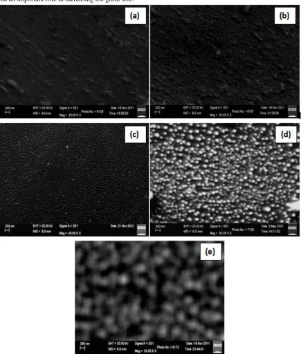
exhibited dense surface and fine grains were observed at 300oC annealed films and the grain size was increased with increasing annealing temperature. It was obvious that the accelerated inter-diffusion between the deposited atoms and the glass substrates might played an important role in increasing the grain size.
Fig. 2: SEM image of of NiO thin films at annealing temperatures (a) 30 0C, (b) 200 0C, (c) 300 oC, (d) 400 oC and (e) 500 oC
Surface Morphology Studies:
Fig. 3: AFM images of NiO thin films Annealed at temperatures 30 oC, 300 oC and 500 oC
The as-deposited films exhibited a very smooth surface, with a mean roughness of 8.81 nm. When the films annealed at 200oC, columnar structures grew independently, building up high mountains and deep valleys on the surface. On further increasing the annealing temperature to 300oC, the density and height of columnar structures increased as well. The formation of columnar structures was ascribed to the grain nucleation and growth during the crystallization process. At higher annealing temperature (500oC), surface roughness of all the films increased due to increasing the columnar structures.
Compositional analysis:
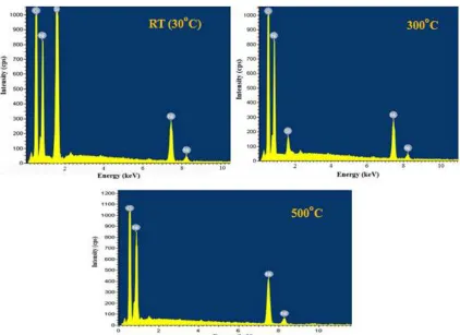
Fig. 4: EDS spectra of NiO thin films at annealing temperatures 30oC, 300oC and 500oC
Optical Properties:
The optical transmittance spectra of the as-deposited and annealed NiO films are shown in Fig. 5 (a). The optical transmittance of the as-deposited film was about 31%. The optical transmittance of the films increased from 39% to 48% with increasing of annealing temperature from 200 to 300oC. On further increasing the annealing temperature to 500oC, the transmittance of the films decreased to 34%.The absorption edge was shifted towards lower wavelength with the increase of annealing temperature.
Fig. 5: (a) Optical transmittance spectra and (b) Plot of (αhv)2 and (hv) of NiO films as a function of annealing temperature
The absorption edge was shifted towards lower wavelength with the increase of annealing temperature. The increase in transmittance of the films was related to an increase in grain size of the films.
Electrical Properties:
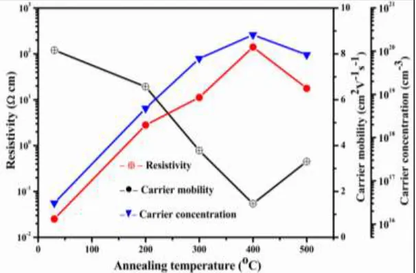
Fig.6 shows the effect of annealing temperature on resistivity, mobility and carrier concentration of NiO thin films. The electrical resistivity of NiO thin films has a strong dependence on the microstructural defects existing in NiO crystallites, such as nickel vacancies and interstitial defects. The increase of carrier concentration, carrier mobility and decrease of resistivity may be due to the improvement of the crystallinity during thermal annealing, which was also evident from XRD studies. Thin film samples annealed at 400oC showed decreased resistivty compared to other samples.
Fig. 6: Behaviour of resistivity, mobility and carrier concentration of NiO thin films as a function of annealing temperature
IV. CONCLUSION
A systematic procedure was adopted in the preparation of NiO thin films using electron beam evaporation technique and the properties of these films were systematically studied at various annealing temperatures. The films annealed at a temperature of 400 oC exhibited single phase columnar growth with better optical and electrical properties which are suitable for sensor applications.
REFERENCES
[1] X.H. Xia, J.P. Tu, J. Zhang, X.L. Wang, W.K. Zhang, H. Huang, 2008, Electrochromic properties of porous NiO thin films prepared by a chemical bath deposition, Solar Energy Materials and Solar Cells 92, 628–633.
[2] L.D. Kadam, P.S. Patil, 2001, Studies on electrochromic properties of nickel oxide thin films prepared by spray pyrolysis technique, Solar Energy Materials and Solar Cells 69, 361–369.
[3] K.K. Purushothaman, S. Joseph Antony, G. Muralidharan, 2011, Optical, structural and electrochromic properties of nickel oxide films produced by sol–gel technique, Solar Energy 85, 978–984.
[4] H. Kamal, E.K. Elmaghraby, S.A. Ali, K. Abdel-Hady, 2004, Characterization of nickel oxide films deposited at different substrate temperatures using spray pyrolysis, Journal of Crystal Growth 262, 424–434.
[5] J.-M. Choi, S. Im, 2005, Ultraviolet enhanced Si-photo-detector using p-NiO films, Applied Surface Science, 244, 435–438.
[6] S. Green, J. Backholm, P. Georén, C.G. Granqvist, G.A. Niklasson,2009, Electrochromism in nickel oxide and tungsten oxide thin films: ion intercalation from different electrolytes, Solar Energy Materials and Solar Cells 93, 2050–2055
[7] A. Mallikarjuna Reddy, A. Sivasankar Reddy, P. Sreedhara Reddy,2011, Thickness dependent properties of nickel oxide thin films deposited by dc reactive magnetron sputtering, Vacuum 85, 949–954..
[8] Y.-S. Lin, P.-W.Chen, D.-J.Lin, P.-Y.Chuang, T.-H.Tsai, Y.-C.Shiah, Y.-C.Yu, 2010, Electrochromic performance of reactive plasma-sputtered NiOx thin films on flexible PET/ITO substrates for flexible electrochromic devices, Surface and Coatings Technology 205, S216–S221.
[9] B.A. Reguig, A. Khelil, L. Cattin, M. Morsli, J.C. Bernède, 2007, Properties of NiO thin films deposited by intermittent spray pyrolysis process, Applied Surface Science, 253, 4330–4334.
[10] S. Pereira, A. Gonçalves, N. Correia, J. Pinto, L. Pereira, R. Martins, E. Fortunato, 2014, Electrochromic behavior of NiO thin films deposited by e-beam evaporation at room temperature, Solar Energy Materials & Solar Cells, 120, 109–115.