Vol. 04, Issue 06 (June. 2014), ||V4|| PP 23-34
Development of RF Remote Control Based Phase Selector System
Oduobuk, Enobong Joseph
1, Idem, Samuel Ntiense
2and Olom, Peter Nkra
31Department of Physics, University of Uyo, Uyo
2,3Department of Electrical Electronics, Cross River University of Technology, Calabar
ABSTRACT:
AnRFremote control based phase selector system was developed. The system is designed with few semiconductors and electromechanical devices. The semiconductor devices includes 555 integrated circuit, 4017 decade counter integrated circuit, transistors and diodes while electromechanical switches used were relays and contactors coupled with other electronic devices. Result shows that, the system starts switching sequentially from one output stage (Phase) to another whenever it senses an RF signal of 300MHz from a VG40T remote control transmitter.KEYWORDS:
Phase Selector, Remote Control, Signal, System, Unit,I.
INTRODUCTION
Today’s study shows that, electricity remain an integral part of our modern society [1]. This is because most domestic and industrial activities in our society are dependent of electricity for its operation. However, electricity has also turned out to be life threatening or sometimes lethal when come in direct contact with. For instance, about (28.8%) of home accident cases related to electric shocks due to direct contact with electricity were reported in Iran [4]. Studies also show that the populations at risk are home-based members of the general public including children, students and retired persons [5]. Sometimes, this electric shock occur when these manually operated or switching equipments or appliances such as manual change over switches, phase change over switches, lighting switches and fan switches are faulty (short circuited). Several ways need to be explored so as to avoid direct contact with electricity driven devices especially during system operation.Although, these devices are insulated, the conductors sometimes become exposed due to wear and tear over time. Unknowingly, when touched during operation, an electric shock must be felt and this can lead to severe injuries or fatality. Therefore, there is need for development of remote control devices so as to avoid direct contact with the system.
Furthermore, physically challenge persons (cripple), aged persons and patients sometimes expierience difficulties in operating home switches especially when there is phase failure and under voltage in the mains of the supply. This is because much stress is involved depending on the location of the switch. Nowadays, remote control based appliances and equipments like air conditioners, ceiling fans and lighting systems are developed so as to address these challenges. However, since such concept is applicable to other systems, hence there is need for the development of remote control based phase selector system. Basically, the specific aim of this project is to develop a phase selector system that is operated with the help of RF remote control. The phase selector is designed to have three phase inputs which include red phase, yellow phase and blue phase. However, the system employs VHF radio remote control VG40T and VG40R modules. The VG 40R is a receiver incorporated into the main system so as to communicate with the VG40T transmitter which is the remote controller [9]. The VG40T transmitter has a single push button which is pressed at each interval as it selects the phases. The phase selector system has a convenient operating range of 15 to 20 meters.
II.
SYSTEM DESIGN
Block diagram
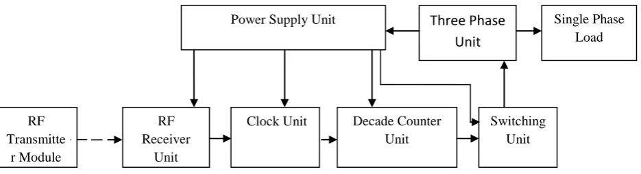
Figure 1.0 Block Diagram of RF Control Based Phase Selector
RF Transmitter Module
This is a Radio frequency remote control transmitter used to communicate with the phase selector. The remote employs VG40 T transmitter module which is powered with a dc voltage (E). It works by pressing the push to-on and off switch ( ) so as to transmit 300 MHz pulse signals [9]. (See figure 1.1)
Ou t In
Ad
j
U2 T Gn d SW1 EFigure 1.1 Circuit Diagram of RF Transmitter Power Supply Unit
This unit converts three phase ac voltage into dc voltage. It consist of transformer ( , and ), diode ( to ), fuse ( , and ) and capacitor ( , and ). In this case, the transformers step down 220V ac to 12V dc. The 12V dc is converted directly to 12V dc with diodes connected in full wave bridge arrangement. Capacitors are also used as filters to smoothen the pulsating dc voltage from the rectifier output as shown in the circuit in figure 1.2.
D15 N D9 D11 D10 D12 T 3 C3 T 1 N D1 D2 D3 D4 D13 C1 T 2 D5 D7 D6 D8 D14 Vcc C2 F1 P1 F2 P2 F3 P3 RF Transmitte r Module
Power Supply Unit
RF Receiver
Unit
Figure 1.2 Circuit Diagram of Power Supply Unit RF Receiver Unit
This is the most important unit in this system which acts as a transducer between the transmitter and the main system. In other words, it converts the radio frequency signals into electrical signal. The components used are VG40R receiver sensor module ( ), transistor ( ), resistor ( , and ), zener diode ( ) and diode ( ). The receiver module requires + 3 volts for operation. Its receiver is designed to receive the 300 MHz signals from the transmitter and is immune to other frequencies [14] [10]. The receiver unit is designed to trigger the base of the transistor with about 300µA causing it to conduct. The zener diode and resistor keeps the input of the receiver module at 3V dc. Also, a diode is employed to keep the signal in forward bias. (See figure 1.3)
R9
Q1 out R8 Vcc
O
u
t
In
Adj
U1 T
+ Gnd
1
2
Dz1 D8
R10
Figure 1.3 Circuit Diagram of RF Receiver Unit
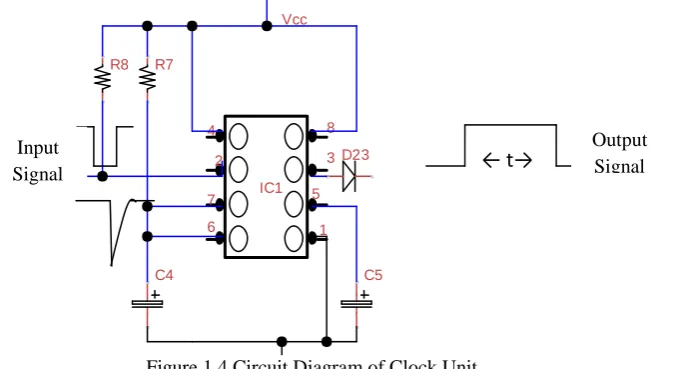
Clock Unit
This is also known as monostable multivibrator unit. It is designed with the popular NE555 timer integrated circuit which is considered as the main brain of this unit. This integrated circuit is configured in a monostable mode as shown in figure 1.4. When the circuit is energized, the output is low and a brief inverted pulse on pin 2 will make the output go high for a period of time determined by the value of and . If pin 2 is low for longer than this period, the output will remain high. In other words, it function is to generate a clock pulse of known width (t) from its output when there is a trigger signal from the preceding blocks of the RF receiver unit. The input signal may be a narrow pulse or a spike. The 555 IC is configured with resistor ( and
), Capacitor ( and ) and diode ( ).
IC1
1
2 3
4
5
6 7
8 D23
C5 C4
R8 R7
Vcc
Figure 1.4 Circuit Diagram of Clock Unit Decade Counter Unit
← t→
InputSignal
This is an extremely useful part of the system. The main component used to design this unit is the CD4017 IC chip which is versatile and relatively fit. This integrated circuit has 16 pins and looks like any other 16 pin integrated circuit. Basically, the decade counter has ten outputs which go “high” in sequence when a source of pulses is connected to the clock input and when suitable logic levels are applied to the reset and enable inputs. In this case the CD4017 IC is connected such that it has only 4 outputs. These are A, B, C and D. During operation, each output goes high whenever a clock from the clock unit comes in through pin 14 (See figure 1.5).
Figure 1.5 Configured Diagram of CD4017 IC Decade Counter Switching Unit
This unit switches on and switches off electrical contacts. The circuit is built with few semiconductor devices, electromechanical switches and other passive components. This includes, npn transistors ( ), relays ( to ), contactors ( ), diodes ( to ), resistors ( to ) and light emitting diodes ( ).For this unit to switch, each base of the npn transistor receives an input from the decade counter and switch the relay which is used to activate the contactor as described in figure 1.5 below.
Figure 1.6 Circuit Diagram of Switching Unit
Three Phase Unit
This is the AC mains from public utility. It supplies 220V to 240V AC to the consumer which is tapped and linked directly to all AC loads. This consist of three phases, namely Red phase ( ), Yellow phase ( ) and Blue phase ( ).
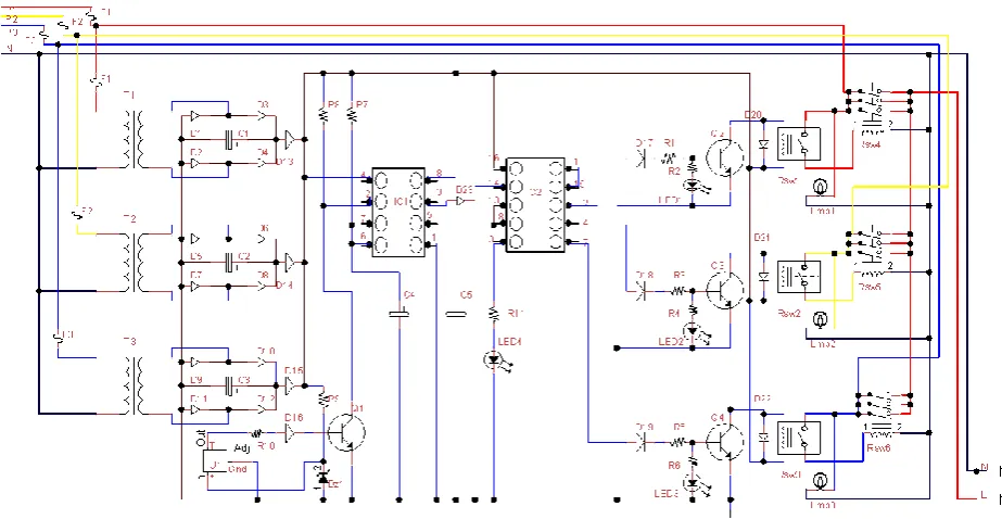
General Circuit Diagram
The circuit diagram in figure 1.6 describes the general design of RF remote control based three phase selector.
Figure 1.6 Circuit Diagram of RF Remote Control Based Phase Selector
III.
CIRCUIT OPERATION
The circuit operation of this system shown in figure 1.6 above is basically a RF remote control based switching system. The system switches from one phase to another when the button in the remote control transmitter is tapped once. In other words, when the transmitter button is pressed, 315MHz signal is transmitted to the receiver which can only decode such frequency signal. In this case, the RF receiver coupled into the main phase selector system act as a transducer. This converts the radiated wave signal into an electrical signal for circuit operation. However, the base of transistor is triggered each time there is signal from the receiver output (T). But, since its collector signal is used as input signal to pin 2 of the NE555 IC, a clock signal is generated across the output at every trigger in the input. This clock signal is basically a square wave signal. At this point, a decade counter start counting each time this clock signal comes in through pin 14. Interestingly, the output signal generated from the decade counter, as a result of the proceeding units is used to switch each phases connected through transistor, relay and contactor. The system also displays it switching state through the present of power indicators. There are; Red ( ), Yellow ( ) and blue ( ) which display the outputs as well as green ( ) for shutdown state. Also the Red ( ), Yellow ( ) and Blue ( ) serve as input indicators.
MATERIALS AND METHODS
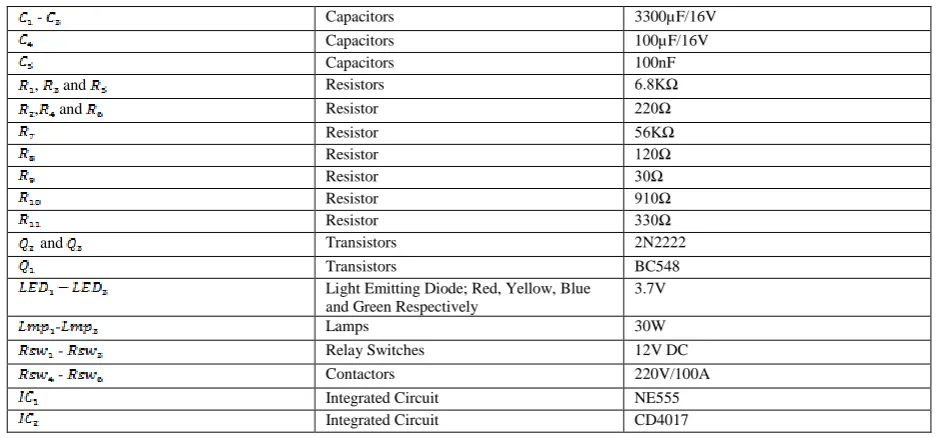
Materials: The materials used in the circuit design are presented in the table in figure 1.0.
SYMBOLS COMPONENTS RATING
- Diodes 1N4001
- , Diodes 1N4148
Zener Diode 5V
- Fuses 1A
E Battery 9V
Receiver Module VG40R
Transmitter Module VG40T
Switch Electronic
- Capacitors 3300µF/16V
Capacitors 100µF/16V
Capacitors 100nF
, and Resistors 6.8KΩ
, and Resistor 220Ω
Resistor 56KΩ
Resistor 120Ω
Resistor 30Ω
Resistor 910Ω
Resistor 330Ω
and Transistors 2N2222
Transistors BC548
Light Emitting Diode; Red, Yellow, Blue
and Green Respectively
3.7V
- Lamps 30W
- Relay Switches 12V DC
- Contactors 220V/100A
Integrated Circuit NE555
Integrated Circuit CD4017
Table 1.0 List of Circuit Components
IV.
METHODS
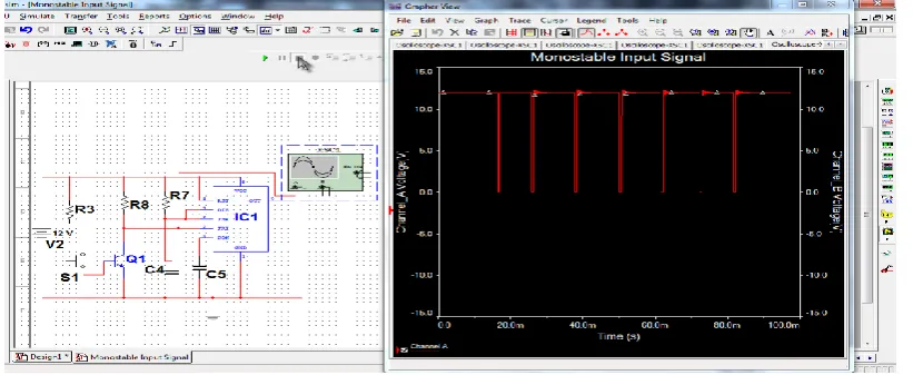
As far as the design function of this system is concerned, the system was evaluated in two most significant ways. This includes; circuit analysis and testing of system units like the RF receiver unit, the clock unit input and output signals and decade counter unit. Moreover, these units were built and tested sequentially so as to evaluate and obtain the signal required for proper operation of the system. The instruments used during the test were Voltmeter and Multisim simulator. (See figure 1.7 (a) and (b). These instruments were used to obtain and achieve an accurate result for proper system operation.
Circuit Analysis Power Supply Unit Peak Inverse Voltage
According to Mehta, the peak inverse voltage is twice the maximum voltage across the half wave[13]; = 2 = 2
Hence PIV = 2 X 12 = 24V
However, the diode used in the rectifier design is 1N4001. This is because it has voltage rating of 50V as required by the circuit.
Average DC Current ( )
The average DC current was calculated using the expression [11];
= (1)
A 200Ω load resistance was considered across the outputs. Root mean square (R.m.s) of the secondary = 12V
Maximum voltage across the secondary ( ) = 12 x = 17V
Dc current flowing through the load ( ) = = = 54mA
Average dc voltage across the load ( ) = x = 54mA x 200Ω = 10.8V
However, the values of dc voltages ( ) and currents ( three phases were equally 10.8Volts and 54mA respectively.
Filter capacitors ( , and );
The filter capacitors were calculated using the expression [11];
C = (2)
But for full wave rectifier circuit [3]; f = frequency of ripple voltage = 50Hz y = Ripple factor = 5% = 0.05
R = = 120Ω
C = =
C = 481µF
Since 481µF capacitor is not standard, instead 470µF was the closest and standard value used as ( , and ).
RF Receiver Unit
Transistor Base resistance ( )
The value of ( ) and ( ) were chosen to be 100mA and 5mA respectively according to the BC548 NPN transistor data book [8].
= (3)
=
= 860Ω
Since the 860Ω resistor is not a standard value, instead 910Ω was found to be the closest and standard value for .
For :
Recall that; = (4)
=
= 120Ω
Maximum Zener Diode Current ( )
Recall that the VG40R receiver requires 5V across it terminal. To achieve this, 5V 1W zener diode is employed into the design.
But for maximum zener current ( ); = (5)
Where; = Maximum Current of Zener Diode
= Power Rating of the Zener diode
= Voltage Rating of the Zener Diode
=
= 200mA
But the maximum value of resistor connected in series ;
= (6)
= 29Ω
In this case, the value of was not found to be standard, instead 30Ω resistor was used.
Zener diode Current ( )
To calculate the value of current flowing through the zener diode ( ) at 100Ω resistance load, we apply;
= (7)
=
= 5mA
Zener diode Current at Full Load ( )
= (8)
= (200 – 5) mA
= 195mA
Clock Unit
Output Clock Pulse Width (t)
Using the equation for charge capacitor [12],
e = E ( ) (9)
Where; e = Capacitor Voltage (in volt) E = Supply Voltage (in volt)
= Base for Natural logarithms (approximately 2.718) t = Time taken for Capacitor to charge (in seconds).
Recall that in the 555 IC, the capacitor charges until it voltage reaches ( ) +Vcc before it discharges through pin
7. Therefore, the ratio becomes; =
Hence, equation (9) becomes
= ( ) (10)
= ( )
By simple rearrangement we have;
- 1 =
=
Multiplying both sides by -1 and taking natural logarithm of both sides, we are arrive at; In( ) =
In(0.333) =
-1.0996 =
Multiplying both sides by -1 we arrive at;
1.0996 =
t = 1.1 R C (11) Note: R = and C =
But the values of and were chosen to be 56KΩ and 100µF respectively. Therefore, equation (11) becomes;
t = 1.1 x x (12)
t = 1.1 x 1KΩ x 1µF t = 1.1ms
Theoretically, the time taken for the capacitor to charge is 1.1 ms.. In other words, this is the output clock signal time (t) and it depends on manual trigger from the proceeding RF unit.
Switching Unit Load Resistance ( )
From Ohm’s law expression [7],
V = IR (13)
By transformation,
= x (14)
Where; Supply Voltage ( ) = 10.8 V Average dc current ( ) = 54mA Load Resistance ( ) = ? Therefore,
= =
= 200Ω
Hence, the relays whose coil resistance is 200Ω were used in the design.
Base Current ( )
Using the expression [13];
= x (15)
Where; = 54mA
= 35
= =
= 1.5mA
Base Resistances ( , and )
By transforming equation (3) in terms of , and ;
= - (16)
=
=
= 6.7KΩ
Current limiting Resistors ( , and )
Using the relationship to evaluate;
= (17)
Where; Supply Voltage ( ) = 10.1V
LED Voltage ( ) = 3.7V
Maximum Allowable Current ( ) = 35mA
X = 2, 4, 6
= =
= 182Ω
Resistor with 182Ω resistance was not found as standard value, the closest standard value obtained was 200Ω and it was used as , and .
However, since light emitting diodes are current driven devices, it will proper calculate the current drawn by each LED;
= (18)
=
= 51mA
Hence, the amount of current drawn by each LED is 51mA.
V.
RESULTS AND DISCUSSION
The following signals in figure 1.7 (a), (b) and figure 1.8 obtained from the oscilloscope describes the nature of the signals at each important unit in the system.
Figure 1.7 (b) Timing Clock output Signal
0
Clock Pulse
Q0
Q1
Q2
Q3
V
o
lt
a
g
e
(
V
)
Time (ms)
1 2 3 4 5 6 7 8 9 10 11
-t--t-
-t--t-
-t-H
L
L
L
L
L H
H
H
H
-t--t-
-t-Figure 1.8 Timing diagram of the System
which indicate that only phase one (Red phase) is “ON”. But, since the system is configured to operate in a sequential mode, the output will also become “HIGH” if another shot is fired from the clock unit. Consequently, output will continue to remain “LOW” until it receives a clock signal. Assuming the state of the system was at output , and the another clock comes due to the signal from remote control transmitter, it will switch back to output since the next output stage is configured so as to reset the system as shown in figure 1.5 and 1.6. Hence, the system will shut down and wait for another clock signal to continue the switching if necessary.
VI.
CONCLUSION
It is magnificent to see that the arrangement of active and passive devices in this work has led
successfully to the development of RF Remote Control Based Three Phase Selector System. The system is able to change from one phase to another once it received an RF Signal. The RF remote control based phase selector prototype is unique in nature. The system reduces stress, durable, maintenance free, very effective because of moderate switching speed and easy to operate.
Finally, it is recommended that such system should therefore be incorporated into residential buildings and other electrical installation where aged and physical challenge people resites so as to address the immediate problems including electrical hazards associated with switching systems.
REFERENCES
[1] Ardeshir S., Mehrzad K. and Mahammad H. G., Electrocution-Related Mortality. Am journal Forensic Medpatol
www.amjforensicmedicine.com, 2010, 31(1), Pg 1-8
[2] Amplifier Transistor NPN. Silicon. Motor Role Semiconductor Technical Data. www.datasheet360.com Retrieved 24/05/2014 [3] Colin Mitchell, Talking Electronics. www.talkingelectronics.com, 2012, 1-12, Retrieved: 10/03/2014
[4] Electrical Safety and you, Health Safety and Executive, www.hse.gov.uk/pubns/indg231.htm, 2013, 1-6, Retrieved: 11/03/2014 [5] Ken Bowron, Electrical Incident Safety Report. www.energysafety.wa.gov.an. 2012, 1-44 Retrieved: 05/05/2014
[6] Light Emitting Diode. www.wikipedia.org/wiki/light-emitting_diode Retrieved 11/04/2014
[7] Mehta, V. K. and Mehta, R. Principle of Electronics. New Delhi. Indi: S. Chand & Company Ltd, 2008, 234-440.
[8] NPN Epitaxial Silicon Transistor, Fairchild Semiconductor Corporation, www.fairchildsemi.com 2014, Retrieved 12/05/2014 [9] Pradeep G. Radio Remote Control. Electronics For. (20), 2005, 173-189
[10] Rabidra N. and Sharma N. ” Wireless Calling Bell” www.electronicsmaller.compdf, Retrieved; 09/05/2014 [11] Theraja, B. L. Basic Electronics. New Delhi, India: S. Chand & Company Ltd, 2009, 178-388
[12] The 555 Internal and Basic Operation. www.play-hookey.com Retrieved: 05/05/2014
[13] Using Transistor as a switch (2014). Microcontrollers and Electronics Project Blog. www.ermicro.com/blog, Retrieved 24/05/2014