Volume-5 Issue-1
International Journal of Intellectual Advancements
and Research in Engineering Computations
A novel approach to detect & prevent hardware
trojan attacks for trusted
integrated circuits
Jeyachandran.M
Research Scholar, Nandha Engineering College, Erode, Tamilnadu, India - 638052
Sukumar.P
Associate Professor, Nandha Engineering College, Erode, Tamilnadu, India - 638052
Abstract : Hardware trojan detection and prevention is paid more and more attention in recent years due to the great potential threat imposed by hardware trojan to the whole integrated circuit industry. Using a combination of new design techniques and new memory technologies, we present a new approach that detects a wide variety of hardware Trojans during IC testing and also during system operation in the field. It can also prevent a wide variety of attacks during synthesis, place-and-route, and fabrication of ICs. It can be applied to any digital system. This project demonstrate its applicability for both application-specified integrated circuits and field-programmable gate arrays. Using fabricated test chips with Trojan emulation capabilities and also using simulations, we demonstrate: 1) our approach can prevent 99.98% of specific attacks (simulated) that utilize detailed knowledge of the design being attacked 2) our approach never produces any false positives, i.e., it does not report attacks when the IC operates correctly.
.
Keywords — Hardware Trojan, C432, Concurrent Error Detection, LSFR, CLB, Flipflop, Detection & Prevention of IC’s.
1. INTRODUCTION
With the globalization of integrated circuit (IC) supply chain, more and more IC designers outsource their design to IC manufacturers. Then ICs are exposed to threat from potential attackers. Attackers may insert extra circuits called hardware trojans in good ICs (golden ICs). These Trojans stay quiet mostly and can be triggered in some way. Once triggered, trojans can execute some malicious operations.
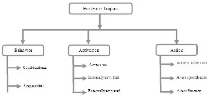
Trojans are classified based on behavior, activation and action. Each of them is discussed below in detailed (Figure 1).
Figure 1: Classification of Hardware Trojan
1.1 Behavior
Malicious circuit design inserted can be subdivided based on the type ofdesign implementation. It can either be combinational design or sequential designs. Firstly, combinational designs are implemented only with Boolean logic gates as shown in Figure 2. Here the Trojan circuit is only activated when a=0, b=1 and c=1, otherwise the circuit operates without any malfunction. Once a special test pattern enables the Trojan logic, output of S‟ is altered. On the other hand, sequential designs contain memory elements which is on the right side of Figure 2, where counter value is incremented when a=1,b=0 at rising edge of clock. Once counter reaches a specific value the functionality of S‟ is altered.
Figure 2: Trojan – Combinational Circuit.
1.2 Activation:
Combinational and sequential designs are only activated with some special patterns. Based upon method of activation, Trojans are classified as Always-On, Internally activated and externally activated.
Always-On Trojans do not need any special inputs to be triggered i.e. in always-on type a simple ex-or gate can be inserted. An internal signal is connected to one of the inputs and logic „1‟ to another. The result of this type of Trojan is a complement of the internal signal. Internally activated Trojans are not activated till specific condition is met .i.e. Trojans can be activated only with special patterns. Activated Trojan modifies the functionality of designs. In externally activated, the adversary drives an external signal to activate Trojans.
Figure 3: Simple XOR gate
1.3 Action
Activated Trojan can either bypass key information of user, named as transmit information, alter function or specifications. It describes a modify function, Trojan alters chip function by adding an extra logic or destroying entire chip, whereas modify specification Trojans alter properties like delay by modifying transistor parameters. Transmit information type Trojans may compromise sensitive information either by radio emissions or through covert channels built at the output of altered circuit.
This paper presents a detection and prevention of Trojan architecture for digital systems, which enables test-time and runtest-time detection of Trojans inserted during fabrication. Insertion of Trojans during fabrication based on sophisticated reverse-engineering of the design being fabricated is prevented. Through this approach Trojan insertion during logic synthesis and layout design is prevented.
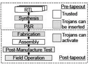
In this paper, we assume that logic synthesis tools, physical design tools, as well as IC fabrication are untrusted, meaning CAD tools and/or foundries can insert Trojans which is shown in Figure 4. However, we do require the RTL or system specification as well as system assembly to be trusted, meaning that an adversary cannot insert a Trojan during these stages.
Figure 4: Assumption on when Trojan can be inserted or activated
The rest of this paper is organized as follows. Section II presents Existing method. Section III introduces our proposed method. Section IV gives experimental results of trojan insertion in FPGA and detection. Finally, Section V concludes this paper
.
2. EXISTING METHOD
2.1 Fingerprinting
In Delay Fingerprinting, these non-destructive techniques detect Trojans by taking delay measurements along certain paths and finding a difference between them and timing for an intended design [5],[6] & [9]. If a Trojan is inserted, the delay may not match the model. While present strategies for inserting test points to make various paths observable, these methods are prone to false positives since Trojans must be distinguished from variability and noise.
Several fingerprinting methods are combined and GLC can be used to compare the results with a model. While stronger, these methods share similar limitations as GLC.
2.2 Split-Manufacturing
A split at the first metal layer (or very low metal layers) can prevent an un-trusted foundry from reverse-engineering a design since most interconnects are missing [1] [2]. However, split manufacturing does not provide Trojan detection by itself. Destructive stress tests on selected back-end-of-line stacks can detect reliability attacks. Trusted monitor chips stacked on top of an untrusted chip using through-silicon vias (TSVs) may be used to actively detect attacks or selected wires may be lifted (using TSVs) to a secure layer to obfuscate a design. Large TSV pitch can lead to area inefficiencies [3].
2.3 Gate Level Characterization (GLC)
Measurements are taken, leakage power or delays of individual gates are estimated, and Trojans are identified. GLC shares the [4] limitations of other fingerprinting techniques.
Trojans can be detected by Electromagnetic radiation (EMR) imaging to search for physical anomalies. This approach does not prevent an adversary from reverse-engineering the design. Scanning Electron Microscopy (SEM) or Focused Ion Beam (FIB) can also be used, but they require delayering the chip, thus destroying it.
2.5 Switching Power Analysis
These techniques detect Trojans by measuring dynamic current waveforms and comparing with a model for an intended design. If there is a significant difference between the two current waveforms, a Trojan is assumed. These methods are prone to false positives since Trojans must be distinguished from variability and noise
3. PROPOSED METHOD
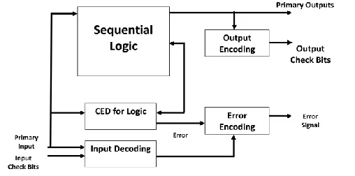
Detection and Prevention of Trojan is derived from the concept of Concurrent Error Detection (CED) for fault-tolerant computing. The “classical” CED approach gives a function, an Output Characteristic Predictor (OCP) predicts an output characteristic (e.g., parity of output bits) for each input to that function. Another function (checker) calculates the actual output characteristic and checks it against the predicted output characteristic. The checker reports an error whenever the two do not match.
Figure 5: a) General Block Diagram for concurrent error detection, b) Separate CED techniques for separate functions of a chip
However, the problem of detecting attacks by hardware Trojans is different than CED for fault-tolerant computing for the following reasons:
1. CED for fault-tolerant computing generally targets single faults (that may occur at random depending on the fault model). For example, CED techniques that predict output parity (or the count of 0‟s or 1‟s in an output word) can be easily compromised if an attacker inserts a hardware Trojan which flips output bits of the function such that the number of 1‟s in a given output word is preserved.
2. An attacker must not be able to derive the OCP; otherwise, the attacker could modify both the function outputs and the OCP outputs such that the checker does not detect errors.
3. CED techniques for fault-tolerant computing generally assume that only one of the units (function, OCP, checkers) is faulty (at any given time). For hardware Trojans, one cannot make such assumptions.
Thus, FPGAs that are manufactured by untrusted foundries can still be vulnerable. Our detection and prevention of hardware Trojan approach overcomes the limitations of classical CED techniques. At the same time, it avoids the high overheads of FPGAs through selective hardware programmability in Trojan checking circuitry. Figure 6 shows a digital system with circuit components vulnerable to Trojan attacks highlighted in red. The system operates in a trusted environment; however, all chips are vulnerable to Trojans. While wires (or channels) between chips may not vulnerable to attacks (since the system may be assembled in a trusted environment), any chip with a Trojan may use them to send incorrect data.
Figure 6: Assumptions on vulnerable system and chip component
As shown in the Figure 6, we assume the system is assembled in a trusted environment. Thus, any Trojan attack within the system will originate from at least one chip. Each chip in the system encodes its outputs and receives encoded inputs. Specifically, Chip 1 outputs data and corresponding check bits so Chip 2 can use them to verify the data. Encoded error signals sent from each chip convey the state of all checkers within the chip. The error monitors then interpret these error signals and determine whether an attack has occurred. Each chip implemented using TPAD includes four modules (Figure 7): input encoding, CED-based Trojan detection, output encoding and error encoding.
Figure 7: System Architecture for each chip
The decoding process checks for attacks at the outputs of the sender as well as attacks at its own inputs. Suppose that, primary inputs and input check bits are received. The input check bits are then XOR-ed with the previous cycle‟s input check bits to calculate the expected randomized parity bits. The actual randomized parity bits are calculated from the primary inputs. Since both sets of randomized parity bits (expected and actual) are equal, no attack has occurred in this case. However, when a pin attack occurs, the expected parity bits will not match the actual bits; thus, the pin attack will be detected.
3.2 Output Encoding:
Detection and prevention of Hardware Trojan Attacks encodes primary outputs using randomized parity encoding. A separate encoding is used for each subsequent chip in the system that receives a different set of the primary outputs; the same encoding is used for chips receiving the same set of primary outputs. The primary outputs and their check bits can be transmitted to destination chips serially (same or different pins) or in parallel.
A randomized parity codeword is calculated for the primary outputs during each clock cycle. The check bits of this codeword are then XOR‟ed with the
previous output check bits (stored in flip-flops), to form the output check bits (e.g., 1101012 ⊕ previous output check bits 0101012 produces output check bits 1000002). The output check bits are then stored and used in the next clock cycle. Thus, the output encoding at a particular time is a function of the history of the primary outputs in the preceding clock cycles (the starting check bits are initialized at chip startup to be uniformly random).
In order for a chip to check its primary inputs, it must use the same randomized parity encoding scheme as the sender‟s output encoding. To ensure this property, FIFOs or proper handshaking protocols may be required.
An attacker can attempt to derive the randomized parity scheme by adding hardware to the chip that stores randomized parity outputs and solves linear equations. However, even an attack that requires fewer additional gates can usually be detected using nondestructive post-manufacture inspections; thus, a complex attack such as this is expected to be detected.
3.3 Logic CED:
On-chip logic is protected using CED as introduced at the beginning of Section II. When the combinational logic is separated into independent blocks, different CED schemes may be used for each of the blocks. These techniques overcome the limitations of classical CED in detecting Trojan attacks.
3.4 Memory CED:
Trojans inserted in an on-chip RAM (e.g. read/write logic, address decoder logic, and memory cells) can alter the data, the location in which the data is stored, or the operation of the RAM (read vs. write). To detect such attacks, the RAM is protected using a randomized parity code. During a write operation, both the address (e.g., BE16) and data bits (e.g., 12416) are used to calculate check bits (e.g., 616) to ensure that correct data is written to the correct location. These check bits are stored along with the data. During read operation, the address (e.g., BE16) and data (e.g., 12416) are used to calculate the expected check bits (e.g., 616). These are ompared with the check bits read out from the memory (e.g., 616) and an attack is detected if they do not match. For example, if the same data and check bits (as the above example) were retrieved during a read operation for a different address (e.g. BF16), the expected check bits would not match the retrieved check bits (e.g. 216 ≠ 616). To hide the randomized parity code construction from adversaries, both the encoder and checkers are protected with switchbox programmability.
For detecting attacks related to a write operation, the RAM must operate in write-though mode, a feature in many RAMs. This means that during a write operation, the data that is being written is sensed and appears at the output of the RAM. Thus, immediately following a write operation, the input and output of the RAM block can be checked for attacks. Latches are used to ensure Data Out only changes during a read operation.
Table I shows the specific checking step that detects a Trojan for each operation (read, write, or idle).
Table 1: Possible Attacks in RAM
3.4 Error Signal Encoding
Error signals from various CED checkers are inherently vulnerable. For example, if a single bit is used to indicate that a Trojan attack has been detected, an adversary can simply attack that bit to indicate no attack. Totally self-checking checkers are also inadequate in detecting Trojan attacks, because an adversary can insert a Trojan into the checker that can make the checker output appear to be valid.
deterministic error signal is needed so that it can be interpreted by the error monitor; thus, a LinearFeedback -Shift-Register (LFSR) is natural for this purpose. The polynomial and seed are made programmable to prevent an adversary from compromising the LFSR during design and fabrication. XOR gates are inserted in a shift register as shown in to ensure that any primitive polynomial of degree L can be realized. Programmability can be realized with RRAM switchboxes for low area cost.
Because of the large number of primitive polynomials for a sufficiently large degree, the probability that an adversary correctly guesses which polynomial will be used during runtime is negligible. If the adversary is able to observe outputs of the LFSR during runtime, the evolution of the error signal may be deduced. However, even an attack that requires fewer additional gates can usually be detected using nondestructive post-manufacture inspections; thus, a complex attack such as this is expected to be detected
Figure 8: Linear feedback Shift Register & Sample CED checker design with r = 3bits
A subset of r bits in the LFSR (Figure 8) of a given design, determined during design time, is used to encode the error signals for the CED checker. This subset can be chosen arbitrarily since the characteristic polynomial and seed of the LFSR are programmable. The checker must operate such that when no attack is detected, the error signal will be equal to the r LFSR bits. If the error signal takes any other value, an attack is detected. The subset of r bits can be different for different chip designs.
3.5 SEQUENTIAL BENCHMARK CIRCUIT
In many industries the standard benchmark circuits are used they will be like ISCAS-85, ISCAS-89 etc are used. The ISCAS-85 represents the combinational circuits and ISCAS-89 represents the sequential circuits. These benchmark circuits are used to examine the latest hardware design and testing of manufacturing approaches and different technologies. A detailed explanation of one of the ISCAS-89 benchmark circuit is S526 given below.
Procedure to remove combinationally redundant faults from a sequential circuit is given. The procedure removes gates, primary inputs, primary outputs and flip-flops, such that the resulting circuit is equivalent to the original circuit. We present experimental results of the application of this procedure to ISCAS-89 benchmark circuits
ISCAS-89 sequential benchmark circuits contain large numbers of combinationally redundant faults, defined as follows.
Definition 1: A fault in a synchronous sequential circuit C, comprised of combinational logic CL and memory elements, is said to be combinationally redundant if it is redundant in the combinational logic CL of C.
While combinationally redundant faults in enchmark
circuits are useful for studies on test generation and redundancy identification and removal there are applications where combinationally irredundant circuits are preferable. For example, the performance of procedures aimed at removing sequentially redundant faults and the performance of synthesis procedures are better demonstrated when the starting point is a combinationally irredundant circuit. In this work, we describe a suite of circuits obtained from the
ISCAS-89 benchmark circuits by removing combinationally redundant faults.
The following steps are executed for stuck at a fault.
Step : 1 Forward implication of the value a on line g is
performed as in [15]. For example, a value 0 on the input of an
AND gate implies the value 0 on its output. If a constant value p
reaches the input
Yi
of a flip-flop FF;, then the valuep
is assigned to the output yi of FFi (this is justified below). Implication continues until no additional values can be implied. Step : 2 Every line carrying a fixed logic value as a result of Step 1 is removed.Step : 3 Lines, gates and flip-flops that remain disconnected as a result of Step 2 are removed
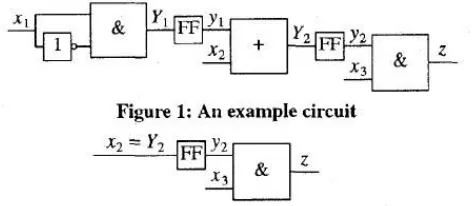
Consider the circuit shown in Figure 1. The fault x1
stuck-at 0 is combinationally redundant. Setting x1 = 0, we obtain Y1 = 0. We then set y1 = 0. No additional implications are possible. The modified circuit is shown in Figure 2.
During the above procedure, some primary inputs, primary outputs, and flip-flops may be removed. The example above demonstrates how primary inputs and flipflops may be removed. A primary output is removed if it takes a constant value as a result of implications. The step where a constant value at the input Y, of a flip-flop is copied to its output y, allows us to eliminate flip-flops from the circuit. Next, we show that the modified circuit is equivalent to the original circuit in the sense.
To demonstrate detection & meren in FPGAs, an FPGA using randomized parity coding to secure the I/O signals was fabricated in 65nm CMOS technology. Since the FPGA is programmable, logic CED can be mapped to the CLBs to protect the FPGA-mapped logic.
However, FPGAs can still be vulnerable to attacks. This FPGA does not contain any accelerator blocks, but the I/O ports of the FPGA still must be protected against pin attacks. Additionally, the memory row decoder needs to be protected. The inputs to the FPGA are encoded with a randomized parity code. This encoding is checked on every clock cycle for errors (Figure. 10).
The design uses 3 check bits for each of the 4 I/O blocks and an additional 3 bits for the memory row decoder, yielding an area overhead of 15% and a power overhead of 0.07% with no critical path delay change. Pin attacks were emulated at the inputs to the chip by selecting random bits of the input stream to be flipped. The checker was monitored to see if the attack was detected. The detection rate for pin attacks was 87.5%, matching the theoretical prediction.
Figure 10: FPGA Pin attack protection
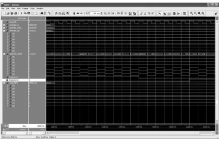
Figure 11: Simulated output – Error Detection
5. CONCLUTION
Detection & Prevention of Hardware Trojan attacks protects digital systems from hardware Trojan attacks through a combination of special concurrent error detection techniques and selective programmability. As a result, it can prevent and detect hardware Trojans with high probability and with no false positives. We demonstrated a variety of detection techniques, from general randomized parity coding (that can be expensive for general designs) to specialized detection techniques (tailored for special functions) that significantly reduce Detection & Prevention of Hardware Trojan attacks area overheads. Hardware test chip results demonstrate the effectiveness and practicality of Detection & Prevention of Hardware Trojan attacks
Software checking techniques that can complement Detection & Prevention of Hardware Trojan attacks for systems supporting both hardware and software programmability will be the future works remains in the system.
REFERENCES
[1] K. Vaidyanathan et al., “Building trusted ICs using split fabrication,” HOST, pp. 1-6, 2014.
[2] K. Vaidyanathan et al., “Efficient and secure intellectual property (IP) design with split fabrication,” Proc. HOST, pp. 13-18, 2014.
[3] C. L. Yu et al., “TSV Process Optimization for Reduced Device Impact on 28nm CMOS,” IEEE Symp. VLSI Tech., pp. 138-139, 2011. [4] S. Wei et al., “Gate characterization using singular value
decomposition: foundations and applications,” TIFS, 7(2):765-773, 2012.
[5] J. Li and J. Lach, “At-speed delay characterization for IC authentication and Trojan horse detection,” HOST, pp. 8–14, 2008.
[6] X. Wang et al.,“IIPS: Infrastructure IP for secure SoC design,” TC, 2014
[7] S. Tamil Selvi., P. Sukumar., “Power Reduction for Sequential Circuit using Merge Flip-Flop Technique”, pp. 926-932, 2014
[8] M. Li et al., “A sensor-assisted self-authentication framework for hardware Trojan detection,” DATE, pp. 1331-1336, 2012.
[9] P. Sukumar., “Low Energy Asynchronous Cam Based On Reordered Search Mechanism,” pp. 74-78, 2015.
[10] T. Maheswari, P. Sukumar., “Error Detection and correction in SRAM cell using Decimal Matrix code,” DATE, pp. 09-14, 2015.
[11] P. Sukumar., “Highly Secured System to Find the Improper Impression of Fingerprints in Hostel,” pp. 92-96, 2016.