Multiple Input DC-DC Converters with Input
Boost Stages
Freddy Gerard
#1, Babu Thomas
*2, Thomas P Rajan
#3#1 PG Scholar, *, 2,3Professor, Department of Electrical & Electronics Engineering
M A College of Engineering, Kothamangalam Kerala, India
Abstract—A high voltage gain DC-DC converter is proposed. This converter is capable of stepping up voltages as low as 20V to 400V. The proposed converter can draw power from four independent sources which makes it suitable for applications like solar panels. The proposed converter finds its application in integration of individual solar panels onto the 400V distribution bus in DC micro grids. The proposed converter consists of Diode-Capacitor voltage multiplier stages. The converters achieve a high voltage gain by charging and discharging of the voltage multiplier capacitors. The design and component selection procedures are presented. The simulation of converter is done using MATLAB/SimulinkR2014 software. A 2W, 10kHz hardware prototype of the base circuit with Vin=1V and Vout=20V is also implemented in the laboratory. PIC16F877A is used for generating the control pulse. mikroC software is used for programming the PIC.
Keywords —DC-DC Converter, Multi Port Converter, Boost Converter.
I. INTRODUCTION
A four input DC-DC converter is proposed for renewable energy applications where several renewable sources are employed. The versatility multiple input converters topologies gives us the advantage of a large variety of connection. Furthermore, the multiport structures extend the opportunity of making the entire system more simple and compact. Multi-port converters have less component count and less conversion stage than the traditional power processing solution which adopts several independent two-port converters. Due to their advantages multi-port converters recently have attracted much attention in academia, resulting in many topologies for applications like integration of low voltage sources to 400V DC microgrid system.
The step-up stage normally is the critical point for the design of high efficiency converters due to the operation with high input current and high output voltage, thus a careful study must be done in order to define the topology for a high step-up application. Theoretically, the conventional boost DC-DC converter can provide a very high voltage gain by
using an extremely high duty cycle. Large duty cycles result in high current stress in the boost switch. Due to large duty ratio parasitic elements has to be considered and their effects reduce the theoretical voltage gain
Some converters can easily achieve high step-up voltage gain. However, transformer volume is a concern. Transformer leakage inductance can produce high voltage stress, increases the switching losses and the electromagnetic interference problems, thus reducing the efficiency of converter. In order to reduce the voltage stress certain measures, have to be considered. Thus, the weight, volume and losses of the power transformer are limiting factors for the isolated DC-DC converters used in embedded applications.
Some other alternative step-up DC-DC converters without step-up transformers and coupled inductors were presented in [2] – [6]. By cascading diode–capacitor or diode-inductor modules, these kinds of DC-DC converters can provide high voltage gain. But the passive elements and switch were under high voltage stress in this cascaded converter.
Non-isolated DC-DC converter topologies using capacitor-diode voltage multiplier cells can be used to, obtain high static gain, low voltage stress and low losses, improving the performance with relation the classical topologies. A high voltage gain dual input converter used voltage multiplier cells integrated with a classical boost converter is proposed was proposed [1]. Several multiplier cells are connected together to boost up the output voltage without compromising the voltage stresses across the components. The main advantage is that voltage gain can be increased by adding of diode capacitor stages. The proposed converter can draw current from four independent sources. So in place of four different converters we can use a single converter. Thus making the process of energy harvesting a very efficient.
II. MULTIPLE INPUT DC-DCCONVERTER WITH
INPUT BOOST STAGES
boost stages at the input. The VM stages are used to help the boost stage achieve a higher overall voltage gain. The voltage conversion ratio depends on the number of VM stages and the switch duty ratios of the input boost stages. This converter is capable of stepping up voltages as low as 20V to 400V. The proposed converter offers continuous input current and low voltage stress (1/4th of its output voltage) on
its switches. Thus offering a gain of 20.
Fig. 1: High-voltage-gain DC-DC converter proposed in [1].
Fig. 2: Proposed multiple input DC-DC converter with input boost stages
Fig. III: A Dickson Charge Pump
III.OPERATING PRINCIPLE
The proposed converter provides a high voltage gain using the modified Dickson charge pump voltage multiplier circuit (See Fig. 3). On a closer look, it can be seen that the converter is made up of two stages. The odd numbered upper stages, which have same mode of operation and the even numbered lower stages, which have same mode of operation.
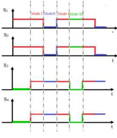
Fig. 3: The switching sequence
For normal operation of the proposed converter, there should be some overlapping time when both the switches are ON and also one of the switches should be ON at any given Therefore, the converter has three modes of operation. The proposed converter can operate when the switch duty ratios are small and there is no overlap time between the conduction of the switches. However, this mode of operation is not of interest as it leads to smaller voltage gains.
.
A. Mode I
In this mode all the switches are ON. All the inductors are charged from their input sources. The current in the inductors rise linearly. The diodes in different VM stages are reverse biased and do not conduct. The VM capacitor voltages remain unchanged and the output diode Dout is reverse
biased Fig. V. Thus the load is supplied by the output capacitor Cout.
B. Mode II
C. Mode III
In this mode switch S2 and S4 ON. Now the even numbered diodes are forward biased and the inductor current flows through the VM stage capacitors charging the even numbered capacitors and discharging the odd numbered capacitors as shown in Fig.7.
Fig. 5: Mode I Operation
Fig. 6: Mode II Operation
Fig. 7: Mode III Operation
IV. VOLTAGE GAIN
The charge is transferred progressively from input to the output by charging the VM stage capacitors. Here V(in1) = V(in2) =V(in3) = V(in4) = V = 20V. And duty ratio of all switches are same and equal to 0.75. From the working of Dickson charge pump.
d
V
V
in out
1
5
(1)
V. DESIGN OF COMPONENTS
The simulation of a converter rated at 400 W with Vin1= Vin2=Vin3 = Vin4=20 V and Vo=400 V is
simulated. So the Output current Io=1A. Switching frequency fsw =100kHz. Number of voltage multiplier (VM) stages, N=4. Duty ratio is given by
0.75 V 1) (N * V V d d d d 0 in 0 4 4 3 1 (2)
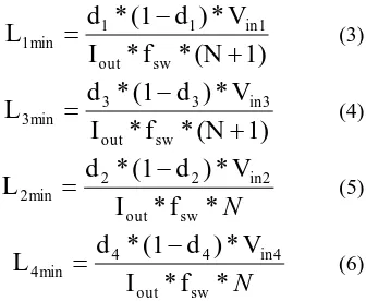
A. Inductor Design
The inductor currents in the boost stages depend on the number of VM stages connected to each leg. The inductor design is similar to that of the normal boost converter. The inductor value is selected such that the boost stages operate in continuous conduction mode(CCM). The minimum inductor value for the CCM operation of the boost stages is given by,
1)
(N
*
f
*
I
V
*
)
d
(1
*
d
L
sw out in1 1 1 1min
(3)1)
(N
*
f
*
I
V
*
)
d
(1
*
d
L
sw out in3 3 3 3min
(4)N
*
f
*
I
V
*
)
d
(1
*
d
L
sw out in2 2 2 2min
(5)N
*
f
*
I
V
*
)
d
(1
*
d
L
sw out in4 4 4 4min
(6)B. Capacitor Design
The output capacitor is selected based on the amount of charge that is transferred to the output for a desired output voltage ripple. Assuming a voltage ripple of 0.02% of output voltage, the required capacitance is given by,
0 sw 0 out
ΔV
*
f
d)
(1
*
I
capacitors with low ESR to minimize the losses, for that purpose thin film capacitors are selected as they have low ESR values.
VI.SIMULATION PARAMETERS
The simulation parameters used for multiple input DC-DC converter are shown in Table I. The duty ratio and input voltage for all the branches are taken same.
TABLE I Simulation parameters
Components Rating
Input Voltage 20V Output Voltage 400V Load Resistance 400Ω Duty Ratio 75% Inductors 100µH VM stage capacitors 20µF Output Capacitor 22µF
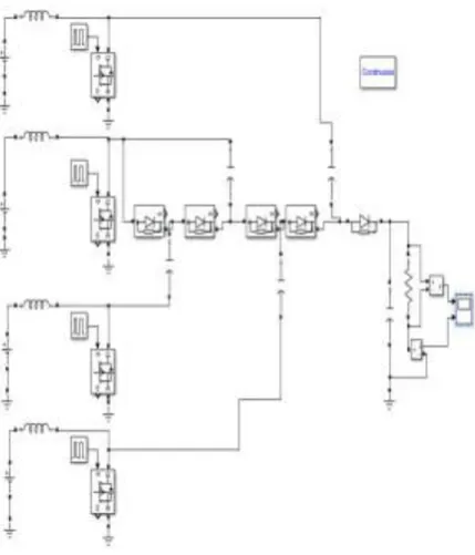
VII. SIMULATION MODEL AND RESULT
A 400W model of converter is simulated in MATLAB/ SIMULINK environment.
Fig. 8: Simulation model of the proposed converter
The switching sequence for S1, S3 are same and
switching sequence of S2, S4 are same.
Fig. 9: Voltage Stress across switch (a) S1 (b) S3 (c) S2 (d) S4
Fig. 9 shows the voltage stress across the switches. A voltage stress of 80V is experiences by the switches. Compared to the output voltage of 400V the value is small (25%). So the switching stress is low.
Fig. 10: Current through inductor (a) L1 (b) L3 (c) L2 (d) L4
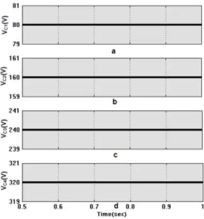
Fig. 11: Voltage across capacitor (a) C1 (b) C3 (c) C2 (d) C4
Fig. 11 shows the voltage across each voltage multiplier stage capacitors. The voltage across each capacitor will be a multiple of 80V. The output of each boost stages will be 80V. Similar to the working of Dickson charge pump [7] the voltage across each capacitor will increase by 80V.
Fig 12 shows the output waveforms of obtained in the simulation. Output voltage is 400V and the output current is 400A. The simulation model is rated for 400W.
Fig. 12: Output (a) Voltage and (b) Current
VIII. EXPERIMENTAL SETUP AND RESULTS
A 2 W, 10kHz prototype of the DC-DC converter with high voltage gain and two input boost stages with input 1V is implemented. Table 2 shows the specification.
TABLE II
Components used for prototype
Components Rating
Inductors 30µH Capacitor 22µF Diode IN5819 Controller PIC16F877A MOSFET IRF540 Driver IC TLP250
Fig. 13: Experimental setup
Fig. 14: Output voltage waveform
frequency and have a duty ratio of 0.75.
IX.CONCLUSION
A high voltage gain DC-DC converter is introduced that can offer a voltage gain of 20, i.e., to step up a 20V input to 400V output. The output voltage, switching stress, inductor current and capacitor voltage are observed. Output voltage of 400V was obtained during the simulation. The observed values from the simulation are similar to the calculated values. Compared to the classical DC-DC converters the voltage stress across switches is low. The voltage across the switch was 80V which is a small value com- pared to the output voltage. The current through S2 shows a spike because of the voltage
imbalance between different voltage multiplier stages. The size of the converter would be less because high frequency operation and absence of winding transformer. On comparing with resonant converter the absence coupled inductor makes this converter superior, since leakage flux and stray magnetic field loss is not present. Since it is a multi-port converter with a high voltage gain, independent sources can be connected and power sharing, MPPT algorithms can be implemented independently at each input port. The main problem associated with the proposed converter is that, as the stages increases the size of capacitor becomes large. Thus making the circuit bulky. The converter finds its application in integration of individual solar panels onto the 400V distribution bus in data centers, telecom centers, DC buildings and microgrids. Hardware prototype of 2W, 10 kHz of the base circuit [1] was implemented.
REFERENCES
[1] V. A. K. Prabhala, P. Fajri, V. S. P. Gouribhatla, B. P. Baddipadiga, and M. Ferdowsi, “A DC-DC Converter With High Voltage Gain and Two Input Boost Stages,” IEEE Trans. on Power Electronics, volume 31, pp. 4206- 4215, 2016.
[2] Zhao and F. C. Lee, “High-efficiency, high step-up dc–dc converters,” IEEE Trans. Power Electronics, vol. 18, no. 1, pp. 65–73, Jan.2003.
[3] R.-J. Wai and R.-Y. Duan, “High step-up converter with coupled-inductor”,IEEE Transactions Power Electronics, vol. 20, no. 5, pp. 1025– 1035,Sep. 2005.
[4] R.-J. Wai and R.-Y. Duan, “High-efficiency power conversion for low power fuel cell generation system,”
IEEE Transactions on Power Electronics, vol.20, no. 4, pp. 847–856, Jul. 2005.
[5] Y. Jang and M. M. Jovanovic, “Interleaved boost converter with intrinsic voltage-doubler characteristic for universal-line PFC front end,” IEEE Transactions Power Electron., vol. 22, no. 4, pp. 1394–1401, Jul. 2007.
[6] A. Z. Rehman, I. Al-Bahadly, and S. Mukhopadhyay, “Multi input DC-DC converters in renewable energy applications: An overview”, Renewable and Sustainable Energy Reviews, Vol. 41, pp. 521-539, 2015.
[7] John F. Dickson, “On-chip high-voltage generation in MNOS integrated circuits using an improved voltage multiplier technique,” IEEE Journal of Solid-State Circuits, vol. 11, Issue: 3, pp. 374-378, Jun. 1976.
[8] Marcos Prudente, Luciano L. Pfitscher, Gustavo Emmendoerfer, Eduardo F. Romaneli, and Roger Gules, “Voltage Multiplier Cells Applied to Non-Isolated DC–DC Converters,” IEEE Transactions on Power Electronics, vol. 23, no. 2, pp. 871–887, Mar. 2008.
[9] Kuo-Ching Tseng, and Chi-Chih Huang, “High step-up high-efficiency interleaved converter with voltage multiplier module for renewable energy system,” IEEE Transactions on Industrial Electronics, vol. 61, no. 3, pp. 1311-1319, Mar. 2014.