Design of Reversible Central Processing Unit
Based on Reversible Logic Gate
Shachchidanand Nagagach, Assistant Prof. Deepak Kumar
M. Tech. Scholar, Department of Electronics and Communication, Vidhyapeeth Institute of Science & Technology, Bhopal, India
Head of Department, Department of Electronics and Communication, Vidhyapeeth Institute of Science & Technology, Bhopal, India
ABSTRACT: Power crisis is a vital problem in today’s world. In recent years, the growing market of electronic systems suffers from power dissipation and delay removal problem. Bennett et al. proved that the one-to-one mapping between the inputs and outputs of reversible circuit drastically reduces the power consumption and delay consumed of a circuit.There are four major design parameters of reversible circuits. First is the gate count which is the number of gate are used in the circuit. Second is the quantum delay. Third is the number of ancilla inputs which are constant inputs which are used to maintain the reversibility of the device. Fourth is the number of garbage outputs i.e. output signals which are not used as inputs to other gates and are only there to maintain reversibility. In this paper the survey of design central processing unit based on reversible gate and parameter.
KEYWORDS: Reversible Gates, Central Processing Unit (CPU), Garbage Output, Quantum Cost
I. INTRODUCTION
Reversible logic could also help to potentially recover and retain a fraction of the signal energy that can be reused for subsequent operations by doing the computation using the forward path and then undoing the computation using the backward path. These concepts have been implemented in CMOS to save significant amount of energy dissipation even close to 90% using the concepts such as reversible energy recovery logic (RERL) etc [1, 2]. Reversible logic has also promising applications in online and offline testing of faults. For example, it has been proved by researchers that for reversible logic circuits, the test set that detects all single stuck-at faults can also detect multiple stuck-at faults [3]. Further, such a logical structure must possess the same number of inputs and outputs and a one-to-one mapping between the input and output states. Any device designed to these constraints is known as a reversible logic device.
A few critical measurements should be considered in the outline of reversible circuits the significance of which should be talked about. The steady contribution to the reversible quantum circuit is called the ancilla info qubit (ancilla information bit), while the trash yield alludes to the yield which exists in the circuit just to keep up coordinated mapping however is not an essential or a helpful yield. Quantum PCs of numerous qubits are to a great degree hard to acknowledge in this manner the quantity of qubits in the quantum circuits should be minimized.
the quantum computers. Thus there is a need of technology independent design and synthesis of reversible logic circuits that are applicable to quantum computing. The reversible circuit has other important parameters of quantum cost and delay which need to be optimized. The quantum cost of a design is the number of 1x1 and 2x2 reversible gates used in its design thus can be considered equivalent to number of transistors needed in a conventional CMOS design.
II. LITRATURE SURVEY
Lafifa Jamal et. al.[1], The research on reversible logic is expanding towards both design and synthesis. Several researchers have been exploring techniques for synthesis of reversible logic circuits and many interesting contibutions have been made. The synthesis of reversible circuits that employ a minimum number of gates and contain no redundant input-output line-pairs (temporary storage channels) is investigated in; Researchers in have used the positive-polarity Reed-Muller expansion of a reversible function to synthesize the function as a network of Toffoli gates; The work in has illustrated the number of garbage outputs that must be added to a multiple output function to make it reversible. Md. Shamsujjohaet al. [2], further a new reversible design method that uses the minimum number of garbage outputs is also proposed; the authors in investigate the problem of optimally synthesizing 4-bit reversible circuits using an enhanced bi-directional synthesis approach. Thus, in synthesis of reversible logic circuits, the optimization in terms of number of ancilla input bits and also the delay are not yet addressed except in the recent work which discusses about the post synthesis method for reducing the number of lines (qubits) in the reversible circuits.
Michael Nachtigalet al. [3], the design of reversible sequential circuits was first introduced in 1988, in which the design of the JK latch was discussed. Later, the design of the RS latch was introduced in. The design uses two cross-coupled reversible NOR gates as used in conventional logic for designing the RS latch. The design was clock less in nature, i.e., there was no enable signal. The NOR gates were designed from the reversible Fredkin gate. The work was limited to the design of RS latch only. In the authors introduced reversible latches such as D latch, T latch, etc., along with their corresponding flip-flops. The flip-flops were designed using master-slave strategy in which one reversible latch works as a master latch and the other works as a slave latch.
Noor Muhammedet al. [4], in researchers have designed the quantum ripple carry adder having no input carry with one ancilla input bit. In the researchers have investigated new designs of the quantum ripple carry adder with no ancilla input bit and improved delay. In the measurement based design of carry look-ahead adder is presented while in the concept of arithmetic on a distributed-memory quantum multicomputer is introduced. A comprehensive survey of quantum arithmetic circuits can be found in. The designs of reversible barrel shifters have also been attempted. The researchers have attempted the design of reversible barrel shifters but these designs are only limited to design a reversible left rotator. The design of reversible left rotators in the existing literature is evaluated in terms of number of reversible gates used, quantum cost, garbage outputs and delay.
Matthew Morrison et al. [5], Among the existing reversible gates, there is no such reversible gate that can help in mapping the equations A · B¯ ⊕ C and A ⊕ B, singly. The equations A · B¯ ⊕ C and A ⊕ B are useful in mapping many arithmetic functions. As an example, the half subtractor performs A-B operation. The output functions of the half subtractor are Borrow = A¯ · B; Difference = A ⊕ B. This dissertation advances the field by proposing a new reversible gate called the TR gate that realizes the functions A · B¯ ⊕ C and A ⊕ B, singly. Using the TR gate, the half subtractor equations can be mapped on a single gate.
III. REVERSIBLE GATES
steady information (CI). Every one of the yields of a reversible circuit need not be utilized as a part of the circuit [8]. Those yields that are not utilized as a part of the circuit is called as trash yield (GO).The number of garbage output for a particular reversible gate is not fixed. The two main constraints of reversible logic circuit is
Fan out not allowed
Feedbacks or loops not allowed.
o BASIC REVERSIBLE GATES
Several reversible logic gates are used in previous design. In figure 1, show the block diagram of two input (A, B) and two output (P, Q) Feynman gate.
In figure 2, show the block diagram of the three inputs (A, B, C) and three output (P, Q, R) Fredkin gate.
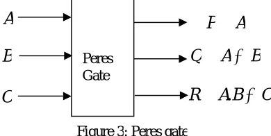
Figure 3 shows the Peres gate. A portion of the 4x4 doors are intended for executing some imperative combinational capacities notwithstanding the fundamental capacities. The vast majority of the aforementioned entryways can be utilized as a part of the outline of reversible adders.
The HNG gate, presented in [10], produces the followinglogical output calculations:
A
P
(1)B
Q
(2)A
P
FG
A
B
Q
A
B
AC
B
A
Q
1
C
B
A
AB
C
A
R
1
FRG
A
P
B
A
Q
C
B
A
C
B
A
R
.
Peres Gate
A
P
Figure 1: Feynman gate
Figure 2: Fredkingate
C
B
A
R
(3))
(
).
(
A
B
C
AB
D
S
(4)The quantum cost and delay of the HNG is 6. At the point when D = 0, the consistent estimations created on the R and S yields are the required total and complete operations for a full snake. The quantum representation of the HNG is exhibited in Fig. 4.
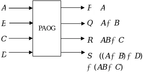
A new programmable 4x4 reversible logic structure Peres And-OR (PAOG) gate is presented which produces outputs
A
P
(5)B
A
Q
(6)C
AB
R
(7))
)
((
).
(
AB
C
C
A
B
D
S
(8)Figure5 shows the block diagram of the PAOG gate. This gate is an extension of the Peres gate for ALU realization.
IV. REVERSIBLE PARAMETER
Some of the reversible gate are NOT Gate, CNOT/ Feynman Gate, Toffoli Gate, Fredkin Gate and Peres Gate. Important parameters of any reversible circuit are as follows:
Gate Count (GC): The number of gates used to realize reversible circuit.
A
P
B
A
Q
C
AB
R
)
(
)
)
((
C
AB
D
B
A
S
A
B
C
D
PAOGGarbage Outputs (GO): The number of unused outputs in a reversible logic. The inputs regenerated at the outputs are not garbage outputs.
Ancilla Inputs (AI): The number of input kept constant at either 0 or 1. Quantum Cost (QC): The cost of the circuit in term of cost of a primitive gate.
Delay: It corresponds to number of primitive quantum gates in the critical path of the circuit.
V. PROPOSED METHODOLOGY
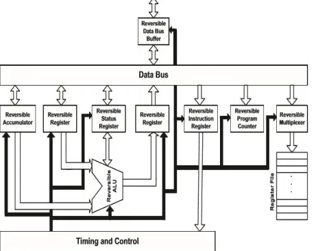
The architecture of the proposed reversible processor is shown in Figure 6. In this figure design the overall structure of the reversible CPU has been divided into small components.
Layout the data bus to handle all of the operations of the reversible CPU.
Design the reversible realizations of the flip-flops.
Design the reversible memory circuits (such as buffer registers and counter circuits) using the proposed reversible flip-flops of the previous step.
Design the arithmetic circuits such as adder, multiplier, divider, comparator etc.
Design the reversible realization of ALU.
Design the reversible control unit of the processor by designing an efficient instruction decoder.
Figure 6: Flow Chart of Proposed Central Processing Unit VI. EXPECTED OUTCOME
The expected outcome has been divided into two sections, i.e. comparison gate in base paper and further work on dissertation part-II.
Comparison Result:-
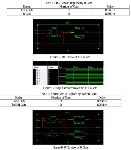
Table I: FRG Gate is Replace by R Gate
Design Number of Gate Delay
FRG Gate 7 8.360 ns
R Gate 5 8.360 ns
Table II: Peres Gate is Replace by Toffoli Gate
Design Number of Gate Delay
Peres Gate 3 8.360 ns
Toffoli Gate 2 8.234 ns
Figure 7: RTL view of FRG Gate
Figure 8: Output Waveform of the FRG Gate
Table 5.3: HNG Gate is Replace by DPG Gate
Design Number of Gate Delay
HNG Gate 7 8.879 ns
DPG Gate 6 8.434 ns
V. CONCLUSION
We have tried the central processing unit is consist of adder, multiplier, divider, memory element, decoder and multiplexer in different reversible gate. The proposed RCPU design will have analyzed on Xilinx 14.1 Spartan-3 and Vertex-7 device family. The proposed design will have compared in terms of maximum combinational path delay (MCPD) and quantum cost with the existing reversible central processing unit (CPU). We can also design 4-bit to 16-bit memory element.
REFERENCES
[1] Lafifa Jamal and Hafiz Md. HasanBabu, “Design and Implementation of a Reversible Central Processing Unit”, 2015 IEEE Computer Society Annual Symposium on VLSI 2015 IEEE.
[2] Md. Shamsujjoha and Hafiz Md. HasanBabu, “A Low Power Fault Tolerant Reversible Decoder Using MOS Transistor”,
2013 26th International Conference on VLSI Design and the 12th International Conference on Embedded Systems.
[3] Michael Nachtigal, and NagarajanRanganathan, “Design and Analysis of a Novel Reversible Encoder/Decoder”, 2011 11th IEEE International Conference on Nanotechnology Portland Marriott August 15-18, 2011, Portland, Oregon, USA.
[4] Noor MuhammedNayeem, Md. Adnan Hossain, Md. MutasimulHaque, Lafifa Jamal, Hafiz M. HasanBabu, “Novel Reversible Division Hardware”, 978-1-4244-4480-9/09/$25.00 ©2009 IEEE.
[5] Matthew Morrison and NagarajanRanganathan, “Design of a Reversible ALU based on Novel Programmable Reversible Logic Gate Structures”, 2013 IEEE Computer Society Annual Symposium on VLSI.
[6] LekshmiViswanath and Ponni. M, “Design and Analysis of 16 Bit Reversible ALU”, ISSN: 2278-0661 Volume 1, Issue 1 (May-June 2012), PP 46-53
[7] Akanksha Dixit and VinodKapse, “Arithmetic & Logic Unit (ALU) Design using Reversible Control Unit”, International Journal of Engineering and Innovative Technology (IJEIT) Volume 1, Issue 6, June 2012.
[8] Mr. Abhishek Gupta, Mr. UtsavMalviya and Prof. VinodKapse, “Design of Speed, Energy and Power Efficient Reversible Logic Based Vedic ALU for Digital Processors”, 2012 IEEE Computer Society Annual Symposium on VLSI.
[9] H. Thapliyal and N. Ranganathan, "A New Reversible Design of BCD Adder," To appear in Proc. Design Automation and Test in Europe (DATE), 2011.
[10] H. Thapliyal and N. Ranganathan, "Design of Reversible Sequential Circuits Optimizing Quantum Cost, Delay, and Garbage Outputs," ACM Journal on Emerging Technologies in Computing Systems, 2010.