Efficient Hardware Design for Computing Pairings
Using Few FPGA In-built DSPs
Riadh Brinci*, Walid Khmiri, Mefteh Mbarek, Abdellatif Ben Rabâa, Ammar
Bouallègue
*(Labortoire Sys’Com, Ecole Nationale d’Ingénieurs de Tunis, 1000 Tunis Email: [email protected])
ABSTRACT
This paper is devoted to the design of a 258-bit multiplier for computing pairings over Barreto-Naehrig (BN) curves at 128-bit security level. The proposed design is optimized for Xilinx field programmable gate array (FPGA). Each 258-bit integer is represented as a polynomial with five, 65 bit signed integer, coefficients. Exploiting this splitting we designed a pipelined 65-bit multiplier based on new Karatsuba- Ofman variant using non-standard splitting to fit to the Xilinx embedded digital signal processor (DSP) blocks. We prototype the coprocessor in two architectures pipelined and serial on a Xilinx Virtex-6 FPGA using around 17000 slices and 11 DSPs in the pipelined design and 7 DSPs in the serial. The pipelined 128-bit pairing is computed in 1. 8 ms running at 225MHz and the serial is performed in 2.2 ms running at 185MHz. To the best of our knowledge, this implementation outperforms all reported hardware designs in term of DSP use.
Keywords-
Cryptography, Field Programmable Gate Array (FPGA), Modular Multiplication, Non-Standard Splitting, Pairing-Friendly Curves1
I
NTRODUCTIONA bilinear pairing is a map × → where and are typically additive groups and is a multiplicative group and the map is linear in each component. Many pairings used in cryptography such as the Tate pairing [1], R-ate pairing [2], ate pairing [3] and optimal pairings [4], choose and to be specific cyclic subgroups of ( ), and to be a subgroup of ∗ .
1.1 Ate pairing
Let be a finite field and let be an elliptic curve defined over . Let be a large prime dividing
# ( ) and k the embedding degree of with respect to , namely, the smallest positive integer such that |( − 1). For any finite extension field of , denote with the -rational –torsion group of the curve. For ∈ ( ) and an integer , let be the infinity point of and !," be a –rational function or Miller function with divisor
!," = s(P) − ( s P) − (s − 1)( )
let = , = ∩ ' ( − ,
where ( is the )* power of Frobenius endomorphism;
( : → (,, -) → (, , - )
and = μ/⊂ ∗
Let ∈ , ∈ and 2 = + 1 − # ( ) be the trace of Frobenius, then,
4( , 5) = ( )6 ,7( ))( 6 )//
is non-degenerate bilinear, and computable pairing, it is the ate pairing
1.2 Pairing-Friendly Curves
An elliptic curve over is called pairing-friendly whenever there exists a large prime |# ( ) with > √ and the embedding degree is small enough, i.e. < <=> ( )/8. Many construction methods result in a parametrized family of elliptic curves, i.e. and are given by the evaluation of polynomials (@) and (@) at an integer value @. One of the most important examples of such families are the Barreto- Naehrig (BN) curves [5], ideally suitable for implementing pairings at the 128-bit security level. These curves have = 12 are defined by
(@) = 36@D+ 36@E+ 24@ + 6@ + 1
(@) = 36@D+ 36@E+ 18@ + 6@ + 1
for some @ ∈ G such that is prime. We show that when we choose @ = 2H + , where is a reasonably small number, the modular multiplication in can be substantially improved.
pairing, the optimal ate pairing on BN curves is defined as [6],
I( , 5)
= ( . K . <L7,7( )M . <N(L7O7),L7( ))( 6 )//
where P = 6@ + 2, = L,7( ) and <Q,R denotes the line through points S and T
Algorithm Algorithm Algorithm
Algorithm 1111 Optimal Ate Pairing over BN Curves
Input Input Input
Input: P =|6@ + 2| = ∑ P!6jkl j2j, ∈ ,
5 ∈ mn ∩ ' (( − )
Output Output Output
Output: o( , 5) ∈ mn
1.p ← 5, ← 1
2.forfor s = − 2forfor downtodowntodowntodownto 0 3. p ← 2p, ← . < , ( ) 4. ifififif Pj=1 thenthenthenthen
5. p ← p + 5, ← . < ,7( ) 6. end ifend ifend if end if
7.end forend for end forend for
8. ← ( . K . <L7,7( )M . <N(L7O7),L7( ))( 6 )// 9.returnreturn returnreturn
Algorithm 1 used arithmetic in mn based on irreducible binomials through a tower of extensions. In our paper we present the towering scheme as:
n= s /(s − z), where z = −1
{= n /( − |), where | = s + 1
mn= { 2 /(2E− ) = n } /(}~− |),
The choice of this towering n→ { → mn makes the final exponentiation much cheaper than other choices. Also we choose ≡ 3 €=• 4 to accelerate arithmetic in n since multiplication by z = −1 is simple subtraction. For BN curve we choose : - =
,E+ 2 and @ = −(2~E+ 857). This choice of curve
parameters will simplify and speed up the reduction phases of the proposed Modular Integer Polynomial Montgomery Multiplier.
1.3 FPGA resources
FPGA manufacturers integrate more and more of dedicated function blocks into modern devices. For example, Xilinx Virtex-6 FPGAs include separate columns of additional function hard cores for memory (BRAM) and arithmetic DSP operations. The DSP blocks are grouped in pairs that span the height of four or five CLBs, respectively. The dual-ported BRAM matches the height of the pair of DSP blocks and supports a fast data path between memory and the DSP elements. Of particular interest is the use of these memory elements and DSP blocks for efficient Boolean and integer arithmetic operations with low signal propagation time. Large devices of Xilinx Virtex-6 class are equipped with up to thousand individual function blocks of these dedicated memory and arithmetic units. Originally, the integrated DSP blocks as indicated by their name were designed to
accelerate DSP applications, e.g., Finite Impulse Response (FIR) filters, etc. However, these arithmetic units can be programmed to perform universal arithmetic functions not limited to the scope of DSP filter applications; they support generic multiplication, addition and subtraction of (un)signed integers [7].
1.4 Outline
The remainder of this paper is organized as follows: Section II studies the most important existing works related to efficient hardware implementations of multiplication over suitable for computing pairings over BN curves. Section III introduces our hardware design of 65 x 65 bit multiplier based on DSP macro for Virtex-6 and performance comparison. Section IV focuses on the hardware implementation and performance comparison of our 258 bit multiplier. Finally, section V provides conclusion and future works.
2
R
ELATEDW
ORKSSince 2009, many hardware implementations of multiplication over suitable for computing pairings on BN curves was described. The first work was described by Fan et al. [8]. Their proposed architecture was based on Hybrid Montgomery Multiplier (HMM) where multiplication and reduction was interleaved. In same year, a new Application Specific Integrated Circuit (ASIC) implementation of pairings over BN curves was proposed. In 2010 Fan et al. [6] proposed a new pipelined and parallelized version of their HMM [8]. In 2011, Corona et al. [9] proposed a new hardware implementation of 258 bit multiplier suitable for computing pairings over BN curves. They used an asymmetric divide and conquer approach to efficiently implement their 65x65 bit multiplier. Their design used only 12 DSP slices on a Xilinx Virtex 6. In same year, Yao et al. [10] proposed a new hardware implementation of optimal ate pairing on Virtex 6. The design computed multiplication over using 32 DSP slices. They combined Lazy reduction with RNS representation.
Algorithm Algorithm Algorithm
Algorithm 2222 Modular Integer Polynomial Montgomery Multiplier (MIPMM) for BN curves
Input Input Input
Input: P(@) = ∑ PjD @j
jkl , …(@) # ∑ …Djkl j@j
(@) # 36@D3 36@E3 24@ 3 6@ 3 1
Output Output Output
Output: †(@) ≡ P(@). …(@). @6‡ €=• (@) 1. Phase 1: Polynomial Multiplication 2.ˆ(@) # ∑ ˆ‰jkl j@j# P(@). …(@)
/*computed by algorithm 3*/
3.Phase 2: Partial coefficient reduction 4.forfor s # 0 toforfor tototo 4
5. Šj# ˆj •s† 2H; j# ˆj €=• 2H 6. ˆjO # ˆjO 3 Šj; ˆj# j . Šj 7. end forend forend forend for
8.Phase 3: Polynomial reduction
9.2(@) # K ˆD3 6 ˆE 2ˆ 6(ˆ 9ˆl) M @D 10. 3 ˆE3 6(ˆ 2ˆ 6ˆl) @E
11. 3( ˆ 3 6(ˆ 2ˆl))@ 12. 3( ˆ 3 6ˆl)@ 13.Œ(@) # 362D@E 14. 336(2D3 2E)@
15. 312(22D3 3(2E3 2 ))@ 16. 36(2D3 42E3 6(2 3 2 )) 17.†(@) # ˆ(@)/@‡3 Œ(@) 18. Phase 4: Coefficient reduction 19. forforforfor s # 0 tototo 3to
20. Šj# †j •s† 2H; j# †j €=• 2H 21. †jO # †jO 3 Šj; †j# j . Šj 22. end forend forend forend for
23.returnreturnreturnreturn †(@)
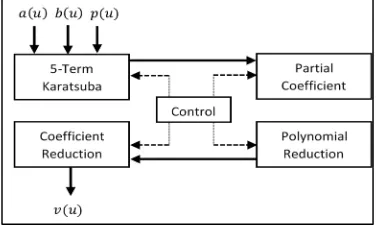
This multiplier consists of 258 bits five terms Karatsuba multiplication which is constructed by one 65x65 bits multiplier basic core. There is registers units to save intermediate results to be used later. The main contributions of this paper are the efficient use of in-built features offered by modern FPGA devices: DSP, adders, subtractors, shift registers… We also designed two variants of basic 65x65 bits multiplier using respectively 7 and 11 DSP slices. Our proposed serialization exploits the independence in each phase and between phases to reduce the cycle count. Figure 1 depicts the top level of the proposed design of Modular Integer Polynomial Montgomery Multiplier for BN curves.
Figure 1 Top level of MIPMM
3.1 Five term Karatsuba Multiplier
The first work to compute Karatsuba using more than three terms was proposed by Peter Montgomery [11]. But it was not suitable for hardware implementation because the large number of addition and subtraction. Corona et al. [9] proposed new scheduling for addition and subtraction to fit hardware design. In this work we propose a more efficient scheduling to achieve one 258 bit multiplication in only 22 cycles. Algorithm 3 describes our Five term Karatsuba Multiplier. This multiplier is based on basic 65 bit multiplier core described in the next subsection
.
Algorithm Algorithm Algorithm
Algorithm 3333 Proposed Five Term Karatsuba Input
Input Input
Input: P(@) # ∑ PDjkl j@j, …(@) # ∑ …Djkl j@j
Output Output Output
Output: ˆ(@) ≡ ∑ ˆ‰jkl j@j 1. l# Pl…l
2. # P … ; ‘l# Pl3 P ; ‘ # …l3 …
3. # ‘l‘
4. E# P … ; ‘ # Pl3 P ; ‘E# …l3 … 5. D# ‘ ‘E
6. ‡# PE…E; ‘D# P 3 PE; ‘‡# … 3 …E 7. ~# ‘D‘‡; ‘~# PE3 P ; ‘’# …E3 … 8. ’# ‘~‘’; ‘‰# ‘l3 ‘D; ‘“# ‘ 3 ‘‡ 9. ‰# ‘‰‘“
10. “# PD…D; ‘l# Pl3 PD; ‘ # …l3 …D 11. l# ‘ l‘ ; ‘ # ‘l3 PD; ‘E# ‘ 3 …D 12. # ‘ ‘E; ‘D# P 3 PD; ‘‡# … 3 …D 13. # ‘ D‘‡; ‘~# ‘D3 PE; ‘’# ‘‡3 …E
14. # ‘ ~‘’
15. ˆl# l
16. €l# 3 l; € # l; 17. ˆ # €l; €“# “3 €l 18. € # 3 ˆ ; €D# “3 E 19. € # D E; €‡# D3 ˆ 20. ˆ # € 3 € ; €E# E3 ‡ 21. # ~ €E; €‰# €E €“ 22. €’# €‡3 ; € # €
23. €~# ‰ ’
24. ˆE# €~ €’; €l# l3 ’ 25. ˆD# €l3 €‰; €E# l 26. ˆ‡# €E € ; € ‡# 3 ‡ 27. ˆ~# €‡ € D; € ~# E
28. ˆ’# €~ € ‡
29. returnreturnreturnreturn ˆ(@)
3.2 Basic 65 bit multiplier core
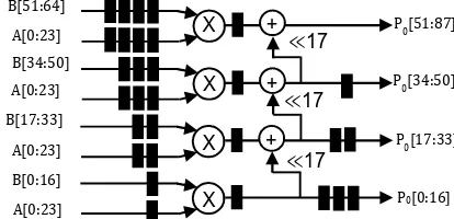
The five term Karatsuba multiplier turned around this module. We propose two different architectures to perform asymmetric multiplication using common non-standard splitting technique. For instance, the asymmetric operands can be computed by the following equation with 25 and 18 bits to fit DSP core of the FPGA. We reserve the most significant bit as operand’s sign. Let
G # ST # (” Pj2j ~D
jkl )(” …j2 j ~D
We decide to not perform full DSP computation for the last core T‡ :~DSl: E to avoid non-useful operations. So, we can write G = Gl+ 2 DG +
2D‰G as described in Figure 2 For example we can
split the operands of Gl as
Gl= Tl: ~Sl: E + 2 ’(T’:EESl: E
+ 2 ’(TED:‡lSl: E
+ 2 ’(T
‡ :~DSl: E)))
In this work we propose two designs called respectively full pipelined and serial architectures depicted respectively. In the first design, we propose three sets of DSP cores arrangement (Zl, Z and Z ): the two first sets have the same design and each set is performed by four DSP slices.
Figure 3 Proposed tilling
The last set is computed by only three slices. We used in the basic core three DSP parameterization detailed as eight 25x18 bit, two 25x15 and one 18x18 DSP configuration. This idea reduces the frequency of the multiplier but let us reduce power consumption by saving extra registers and non-useful operations. This first design achieves one 65x65 bit multiplication in seven cycles using eleven DSP cores.
Figure 4 Proposed hardware design of the first DSP set
The diagram in describes the delay constrained of the full pipelined architecture that takes seven cycles to achieve 65x65 bit multiplication.
Figure 5 delay constrained of the full pipelined architecture
In the second design, we rearrange operations to make
Gl and G share the same hardware. So, we compute
Gl and G in parallel. To get results at same time we added a pipeline stage in the DSP set of G . At the 5)* we have our outputs. In the second cycle, we entered the operands of G to get it at the 6)* cycle. At this time we have also the result of the addition –l= Gl+
2D‰G . The adder is an in-built feature of the FPGA
configured to give result after one cycle. Finally, we performed the last addition, configured also with latency one, giving full result after seven cycles using only seven DSP slices. In this second architecture we have added extra hardware finite state machine, multiplexers and demultiplexers.
3.3 Coefficient and polynomial reductions
The architecture described in
Pipelined
architecture
(b) Serial architectureFigure 6
depicts the top level of each architecture shows the polynomial reduction phase. It can reduce the coefficients one by one taking twelve cycles to achieve the entire reduction. We performed multiplication by using shifts and addition. In this phases, the complexity can be reduced by exploiting the characteristics of the different constants. Since= 2‡(2D+ 2E) + 2~+ (2D+ 2E) + 1,
multiplication by is performed by three additions in three cycles. There is also multiplication by the following constants 6, 9, 12 and36 computed by shifts and additions, e.g. 6P = 2 P + 2P; 9P =
2EP + P;12P = 2EP + 2 P;36P = 2‡P + 2 P;
3.4 Delay constrained of MIPMM
As mentioned before, the 65x65 bit multiplication takes seven cycles to achieve one multiplication. We get all partial products (PP) j∈{l, E} shown in algorithm 3 after 13 cycles. However the delay of datapath for the post partial products combined with PP is two clock cycles. As result, five term Karatsuba gives the first output after 22 clock cycles. As soon as each ˆj∈{l,’} gets out from the pipelined PP core, it is scheduled on the fly to be partially reduced. This phase ends at the 22 second clock cycle. Other reduction phases also combined with phase one take 13 cyclesTherefore, to sum up, the cost of the entire multiplier is 35 clock cycles.
0
24
48
64
34 17
51 64
P10 P9
P0
P3 P2 P1
P4
P7 P6 P5
P9
24 48
B 51:64
B 34:50
B 17:33
X
X
X
X +
≪17
+
+
≪17
≪17
A 0:23 A 0:23 A 0:23 A 0:23
B 0:16
P00:16
P051:87
P034:50
P017:33
Result
Gl
G
5
G
–l
6
–
7 Cycles
–l= Gl+ 2DG
(a) Pipelined architecture (b) Serial architecture Figure 6 Top level design of proposed pipelined and serial architectures
4
P
AIRINGD
ESIGNMost operations in optimal pairing algorithm steps of are performed in mn. Many techniques give efficient computation in extended fields with low complexity. We choose methods with minimum squaring and multiplication. The underlying operations are computed in base field. Therefore we design our coprocessor as scheduling of operations.
As shown in Algorithm 1, Miller loop phase consists of the following major operations:
- Doubling step, is the elliptic curve point doubling combined with the computation of the line <. - Addition step, is the elliptic curve point addition
combined with the computation of the line <. - Squaring of the Miller function .
- Spare multiplication of by < having only half of non-zero coefficients.
We adopt homogenous coordinates proposed in [12] to efficient compute the different curve operations in the Miller loop. The listed above steps need arithmetic in n such as multiplication and squaring. We propose Karatsuba method described by the following equation to compute multiplication.
†l= Pl…l; † = P … ˆl= †l− †
ˆ = (Pl+ P )(…l+ … ) − †l− †
We also refer to complex method to perform squaring in n. First, we precompute †l= PlP . Then, the square ˆ = P is computed as
ˆl= (Pl+ P )(Pl− P ) ˆ = 2†l
Multiplication and squaring operations need respectively 36 and 39 cycles to get out their results. To efficient compute Miller loop we made rearrangements and scheduling in each step to fit our
design. In the doubling step we have to compute three squaring and two multiplications which are equivalent to 12 multiplications in the first part. They takes 48 cycles. In the second part, we have 17 multiplications giving results out in the 94th cycle. The and . < need 111 multiplications computed in 3.885 cycles. To sum up, each Miller loop iteration takes 3.979 clock cycles. Using the same strategy in curve rearrangement addition step is achieved in 3,385 clock cycles. As result, Miller loop takes 277.000 cycles.
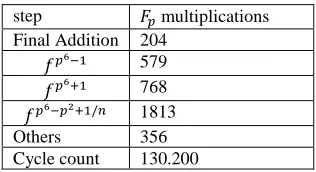
The final exponentiation consists of final addition and final exponentiation. Table 1 gives the different operation in this step and the cycle count.
step multiplications
Final Addition 204
š6 579
šO 768
š6 nO /› 1813
Others 356
Cycle count 130.200
Table 1 Cycle count of the final exponentiation
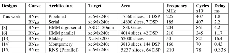
5
R
ESULTS AND COMPARISONThe hole design has been done in VHDL using Xilinx ISE design suite on a Virtex-6 xc6vlx240t-3ff784 FPGA. It used in total 17560 slices, 7 and 11 DSP cores in our serial and pipelined architectures respectively. It runs at 185Mhz and finishes pairing computation on BN curve at 128 bit security level in
2.2 € .
Table 2 lists the performance hardware implementations reported in recent literature. Compared with the other hardware implementation [6] our design saves DSP cores
Gl
DSP set 1
DSP set 2
DSP set 3
+
G ≪24 Sl
Tl
S
T
S
T
+
–l
–
G ≪48
S Sl
S
T T Tl
DSP set 1
DSP set 3
+
G ≪48
–l
–
G ≪ 24
+
0
1
Gl
0
1
1
0
Designs Curve Architecture Target Area Frequency
MHz
Cycles
x103
Delay
ms
This work BN128 Pipelined xc6vlx240t 17560 slices, 11 DSP 225 407 1.8
BN128 Serial xc6vlx240t 14890 slices, 7 DSP 185 407 2.2
[8] BN126 HMM digit-serial ASIC 130mm 183k Gates 204 861 4.2
[6] BN128 HMM parallel xc6vlx240t 4014 slices, 42 DSP 210 245 1.17
[13] BN128 Blakley Xc4vlx200 52000 slices 50 821 16.4
[14] BN126 Montgomery xc6vlx240t 3813 slices, 144 DSP 166 70 0.43
[15] BN126 RNS (Parallel) xc6vlx240t 5237 slices, 64 DSP 210 78 0.338
Table 2 Performance comparison of hardware implementations of pairings at around 128-bit security
until 90%. Our goal is to keep the design of the pairing coprocessor full used by efficient resource sharing at high frequency. It is a serial implementation with minimum area use. The current design not only gains in in-built DSP slices with comparable pairing computation time but also shows that modern FPGA can be able to perform pairing with high complexity at higher security level on different friendly curves with large algebraic closure.
6
C
ONCLUSIONIn this paper we introduce a new hardware design to efficiently serialize polynomial integer multiplication on BN curves over large prime field. Due to deep arrangement and careful scheduling of different steps of the coprocessor our design saves 90% of DSP slices and achieves one pairing computation in 1.8 ms. Our future work will be the multi-pairing computation to respond faster to many client requests. We plan also to implement other curves and different types of pairings on this architecture. Furthermore, we will provide an optimal parameter set and pairing implementations for higher security level including 192-bit or 256-bit security.
R
EFERENCES[1]P. S. L. M. Barreto, H. Y. Kim, B. Lynn, and M. Scott. Efficient Algorithms for Pairing Based Cryptosystems. CRYPTO 2002, volume 2442 of
Lecture Notes in Computer Science, pages 354-368.
Springer, 2002.
[2]E. Lee, H. S. Lee, and C. M. Park. Efficient and Generalized Pairing Computation on Abelian Varieties. Cryptology ePrint Archive, Available from
http://eprint.iacr.org/. Report 2009/040.
[3]F. Hess, N. P. Smart, and F. Vercauteren. The Eta Pairing Revisited. IEEE Transactions on Information
Theory, 52(10), pages 459-462, Oct.2006.
[4]F. Hess. Pairing Lattices. Pairing 2008, volume 5209
of Lecture Notes in Computer Science, pages 18-38.
Springer, 2008.
[5]P. Barreto and M. Naehrig. Pairing-friendly elliptic curves of prime order. Selected Areas in
Cryptography, SAC 2005, LNCS 3897, pages
319-331, 2006.
[6]J. Fan, F. Vercauteren, and I. Verbauwhede. Efficient hardware implementation of Fp-arithmetic for pairing-friendly curves. Computers, IEEE Transactions on, 61(5), 2012, 676-685.
[7]T.Güneysu. Utilizing hard cores of modern FPGA devices for high-performance cryptography, Journal
of Cryptographic Engineering, 1(1), 2011, 37-55.
[8]J. Fan, F. Vercauteren, and I. Verbauwhede. Faster Fp Arithmetic for Cryptographic Pairings on Barreto-Naehrig Curves. CHES 2009, volume 5747 of Lecture
Notes in Computer Science, pages 240-253. Springer,
2009.
[9]C. Corona, C., Moreno, E. F., & Henriquez, F. R. Hardware design of a 256-bit prime field multiplier suitable for computing bilinear pairings.
International Conference on Reconfigurable Computing and FPGAs (ReConFig 2011), 2011,
229-234.
[10]G. X. Yao, J. Fan, R. C. Cheung, and I. Verbauwhede. A high speed pairing coprocessor using RNS and lazy reduction. Cryptology ePrint
Archive, Available from http://eprint.iacr.org/. Report 2011/258, 2011
[11]P. L. Montgomery. Five, six, and seven-term Karatsuba-like formulae, IEEE Transactions on
Computers, vol. 54(3), 362-369
[12]Costello, C., Lange, T., & Naehrig, M. (2010). Faster pairing computations on curves with high-degree twists. In Public Key Cryptography–PKC
2010 (pp. 224-242). Springer Berlin Heidelberg.
[13]Ghosh, S., Mukhopadhyay, D., & Roychowdhury, D. (2010). High speed flexible pairing cryptoprocessor on FPGA platform. Pairing-Based
Cryptography-Pairing 2010 (pp. 450-466). Springer
Berlin Heidelberg.
[14]Ghosh, S., Verbauwhede, I., & Roychowdhury, D. (2013). Core based architecture to speed up optimal ate pairing on FPGA platform. In Pairing-Based
Cryptography–Pairing 2012 (pp. 141-159). Springer
Berlin Heidelberg.