96 | P a g e
IMPROVED EXECUTION TIME FOR 2048 POINT
FFT/IFFT
1
Upasana Sharma,
2Waffa Choudhary
1,2Electronics & Communication Department,
ABES Engg. College, Ghaziabad.(India)
ABSTRACT
This paper represents 2048 point Fast Fourier Transform and its inverse (FFT/IFFT). The modified
architecture provides concept of local ROM module and variable length support from 128~2048 point for
FFT/IFFT and for the designing of this we use UMC of 0.18µm. Start up time for the chip is N/2 clock cycle
where N is the length of FFT/IFFT. 16 bit word length with fixed point precision is used for entire
implementation. And our proposed method can be used in various applications such as Wi-Fi MAX with
enhanced speed.
Keywords: FFT, IFFT, Pipelined Architecture, SDF.
I INTRODUCTION
As FFT is a very fast computing algorithm and thus, is used in various applications such as mobile Wi-MAX, which uses OFDMA [1]. FFT/IFFT is one of the important blocks used in the OFDMA systems. By adjusting length of FFT from 128 to 2048, it can be used for different applications. FFT architectures are mainly classified in two ways:
(i) Memory based architecture (ii) Pipelined based architecture.
Popular pipelined architectures are based on radix-2 or radix-4 algorithms. Higher the radix, lower the computational complexity. Thus, Radix-4 has less computational complexity compared to radix-2 architecture. So, a tradeoff for the selection of architecture is the requirement of length of FFT for the particular application.. Pipelined architectures, on the otherhand, are further classified in two types:
(i) SDF (Single Delay Path Feedback) (ii) MDC (Multiple Delay Path Commutator).
MDC are widely used for MIMO OFDM techniques as one can simultaneously operate on channels. Also MDC make use of less number of delay elements but larger number of storage elements as compared to SDF [2]. Single stage block diagram of R2SDF (Radix-2 SDF) and R4MDC (Radix-4 MDC) is shown in fig. 1, where F is FIFO. BF2 and BF4 stands for two point and four point butterfly unit respectively. D is the delay element.
Fig 1(a): R2SDF Basic Module Fig 1(b): R4MDC Basic Module
II BASIC FFT ALGORITHM
The DFT for N point sequence x(n) is defined as
𝑋 𝑘 = 𝑥 𝑛 . 𝑊𝑁𝑛𝑘 𝑤ℎ𝑒𝑟𝑒, 𝑊𝑁= 𝑒−𝑗 2𝜋 𝑁𝑎𝑛𝑑 𝑘 = 0 … … . . , 𝑁 − 1
𝑁−1
𝑛=0
Where x(n) and X(k) can be the complex number. For the calculation of this transform we requires N2 complex multiplication and N(N-1) complex addition. In order to reduce the computational complexity various algorithm has already been invented like, Cooley and Tukey proposed an efficient algorithm [3]. Afterwards radix-2, radix-4, radix-22[4], split radix [5] and extended split radix [6] have been developed to reduce the computational complexity of FFT. The Signal Flow Graph i.e SFG of 8-point FFT using radix-2 algorithm is shown in fig. 2.
x0 X0
x1 X4
x2 W88 X2
x3 W28 X6
x4 W80 X1
x5 W18 X5
x6 W28 W88 X3
x7 W38 W28 X7
Fig2: Signal Flow Graph of 8point FFT Using Radix-2 Algorithm
98 | P a g e
III PROPOSED ARCHITECTURE
3.1 Single Delay Path Feedback (SDF)
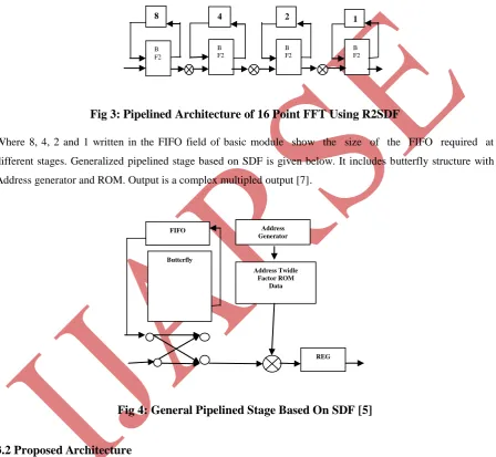
Basic module of SDF is shown in fig. 1(a). Where first N/2 input samples are stored in FIFO and operation starts when N/2+1st data is available at the input to the butterfly unit. For designing N-stage pipelined FFT/IFFT architecture same SDF module is repeated for log2N time. SFG shown in fig. 2 can be implemented
using R2SDF. Block diagram for the same is shown in fig. 3.
Fig 3: Pipelined Architecture of 16 Point FFT Using R2SDF
Where 8, 4, 2 and 1 written in the FIFO field of basic module show the size of the FIFO required at different stages. Generalized pipelined stage based on SDF is given below. It includes butterfly structure with Address generator and ROM. Output is a complex multipled output [7].
Fig 4: General Pipelined Stage Based On SDF [5]
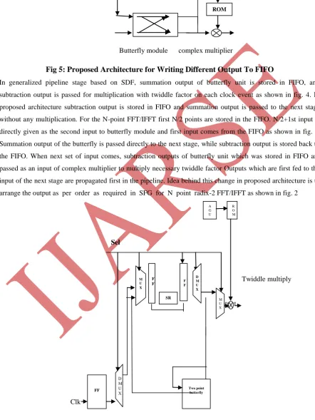
3.2 Proposed Architecture
Modification in generalized pipeline stage is done by modifying FIFO design to enhance the throughput of the design. At different stages of the design, requirement of FIFO is different. Length of FIFO depends upon in which stage of pipeline it is used, where width of FIFO depends upon word length used. In proposed architecture we have chosen word length as 2 x 16 bits. So, width of FIFO is 32 bits. As, suggested in [7], we need to store first N/2 input points in FIFO. This brings the clarity to design different sized FIFO. For N-point FFT/IFFT size of FIFO for the first stage is N/2 x 32 bits, for second stage N/4 x 32 bits, so on and so forth till the end of pipeline architecture. Read and write clock of FIFO is taken on different events. This helps to
8 4 2 1
B F2
B F2
B F2
B F2
FIFO
Butterfly
Address Generator
Address Twidle Factor ROM
Data
improve the throughput for the pipelined architecture. Read and write operations are explained in more detail in section 5.
Butterfly module complex multiplier
Fig 5: Proposed Architecture for Writing Different Output To FIFO
In generalized pipeline stage based on SDF, summation output of butterfly unit is stored in FIFO, and subtraction output is passed for multiplication with twiddle factor on each clock event as shown in fig. 4. In proposed architecture subtraction output is stored in FIFO and summation output is passed to the next stage without any multiplication. For the N-point FFT/IFFT first N/2 points are stored in the FIFO. N/2+1st input is directly given as the second input to butterfly module and first input comes from the FIFO as shown in fig. 5. Summation output of the butterfly is passed directly to the next stage, while subtraction output is stored back to the FIFO. When next set of input comes, subtraction outputs of butterfly unit which was stored in FIFO are passed as an input of complex multiplier to multiply necessary twiddle factor Outputs which are first fed to the input of the next stage are propagated first in the pipeline. Idea behind this change in proposed architecture is to arrange the output as per order as required in SFG for N point radix-2 FFT/IFFT as shown in fig. 2
Sel
Twiddle multiply
output
Clk
SR AGU
ROM
FF
D M U X
SR
Two point butterfly
F
F FF
D M U X M
U X
M U X A G U
100 | P a g e RTL diagram for the proposed architecture is shown in fig. 6. AGU (Address Generation Unit) which generates read address for the ROM. Through which particular twiddle factor is passed for the multiplication
IV IMPLEMENTATION
4.1 AGU & ROM Design
Address Generation Unit generates different sets of addresses for performing FFT and IFFT. Counter is implemented inside AGU. One control signal for the selection of FFT or IFFT is provided. ROM contains all twiddle factors for performing FFT/IFFT. Block diagram for the same is shown in fig. 7.
FFT/IFFT
clk
reset
AGU ROM
Fig7: Block Diagram Of Twiddle Generation
V RESULTS & COMPARISION
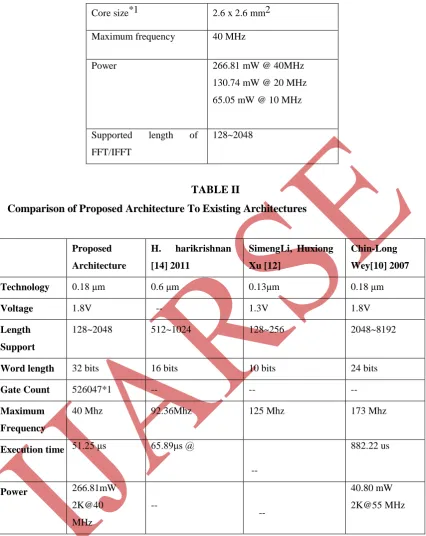
Design for 2048-point is implemented using 0.18 µm Faraday standard cell library from UMC. Flow is completed using encounter. Table 1 lists all implementation results of the chip. Table 2 shows the comparison results of proposed architecture to existing architectures. Gate level netlist` generated from design vision is imported in Encounter tool from Cadence.
As compared to memory based architecture suggested in [10], our architecture takes more hardware but execution time is drastically reduced in proposed architecture, because memory based architecture uses only one butterfly unit and one complex multiplier. So, it helps to reduce the area, but at the same time execution speed is affected by large amount.
TABLE 1.
Implementation Results of Proposed Architecture
Technology UMC 0.18 µm Faraday
Voltage 1.8 V
World Length 16 bits
Gate count*1 526047
Cou nter
M U X
M U
Core size*1 2.6 x 2.6 mm2
Maximum frequency 40 MHz
Power 266.81 mW @ 40MHz
130.74 mW @ 20 MHz 65.05 mW @ 10 MHz
Supported length of FFT/IFFT
128~2048
TABLE II
Comparison of Proposed Architecture To Existing Architectures
Proposed
Architecture
H. harikrishnan
[14] 2011
SimengLi, Huxiong
Xu [12]
Chin-Long
Wey[10] 2007
Technology 0.18 μm 0.6 μm 0.13μm 0.18 μm
Voltage 1.8V -- 1.3V 1.8V
Length
Support
128~2048 512~1024 128~256 2048~8192
Word length 32 bits 16 bits 10 bits 24 bits
Gate Count 526047*1 -- -- --
Maximum
Frequency
40 Mhz 92.36Mhz 125 Mhz 173 Mhz
Execution time 51.25 μs 65.89μs @
--
882.22 us
Power 266.81mW
2K@40 MHz
--
--
40.80 mW 2K@55 MHz
*1 Gate counting including all local ROM Module *2 Area after Synthesis
*3 Excluding RAM
102 | P a g e Here in my proposed architecture the input word size if 32 bits hence the area is little bit more than others [12], [10] yet area is also improved if we compare our result for the current paper [14].
Other then this, post synthesis area for the proposed architecture is 6.76 mm2. Architecture in [12] has variable length of 128 and 256 point only, while proposed architecture has all variable length from 128 to 2048 point. Although the gate count of proposed architecture is higher than others because of dedicated ROM module for each stage of pipeline, yet it certainly helps to improve the execution time.
REFERENCES
[1] WiMAX Forum, Mobile WiMAX-Part I: A technical overview and performance evaluations, Feb. 21, 2006 [2] Bo Fu, Paul Ampadu, “An Area Efficient FFT/IFFT Processor for MIMO-OFDM WLAN 802.11n” J Sign
Process Syst (2009) 56:59–68
[3] J. W. Cooley and J. W. Tukey, “An algorithm for the machine calculation of complex Fourier series,” Math. Comput., vol. 19,Apr. 1965, Page(s):297 – 301.
[4] M. Vetterli and P. Duhamel, “Split-radix algorithms for length- pn DFT’s,” IEEE Trans. Acoust., Speech, Signal Processing, vol. 37,pp. 57–64, Jan. 1989
[5] Soo-Chang Pei, Tzyy-Liang Luo, “Split-radix generalized fast Fourier transform,” Signal Processing, 54(1996) 137-151.
[6] Daisuke Takahashi, May 2001 “An Extended Split-Radix FFT Algorithm,” IEEE Signal Processing Letters,” vol. 8, no.5, pp. 145-147
[7] Erling H. Wold “Pipelined and Parallel-pipelined FFT FFT processor for VLSI Implementation” 0018-9340/84/0500- 0414$01 .00 © 1984 IEEE
[8] Hyun-Yong Lee, In-Cheol Park “Balanced Binary-Tree Decomposition for Area-Efficient Pipelined FFT Processing” 1549- 8328/$25.00 © 2007 IEEE
[9] Jen-Chih Kuo, Ching-Hua Wen, Chih-Hsiu Lin, An-Yeu Wu, “VLSI Design of Variable –Length FFT/IFFT Processor for OFDM-Based Communication Systems” EURASIP Journal on Applied Signal Processing 2003:13, 1306-1316
[10] Chin-Long Wey, Wei-Chien ang and Shin-Yo Lin “Efficient VLSI Implementation of Memory-Based FFT processors for DVB-T Applications” IEEE Computer Society Annual Symposium on VLSI(ISVLSI’07) [11] B. Sklar, “Digital Communications, Fundamentals and Applications, Second Edition, New Delhi, Pearson
Education, 2004.
[12] Simeng li, Huxiong Xu, Wenhua Fan, Yun Chen, Xiaoyang Zeng 2010“A 128/256-Point Pipeline FFT/IFFT Processor for MIMO OFDM System IEEE 802.16e” 978-1-4244-5309-2/10/$26.00 ©2010 IEEE
[13] J.A. Heller and I. M. Jacobs, “Viterbi Decoding for Satellite and Space Communications”, IEEE Trans. Commun. Technol., vol. COM19, no. 5, 1971
[14] K.Harikrishna 1, T. Rama Rao 2, Vladimir A. Labay 2011“FPGA Implementation of FFT Algorithm for IEEE 802.16e (Mobile WiMAX)” International Journal of Computer Theory and Engineering, Vol. 3, No. 2,