A Novel WL-Integrated Low-Insertion-Loss Filter with Suspended
High-
Q
Spiral Inductor and Patterned Ground Shields
Tao Zheng1, 2, Mei Han1, 2, Gaowei Xu1, and Le Luo1, *
Abstract—A novel wafer level integrated low-insertion-loss filter working at 1.8 GHz (DCS LPF) with suspended inductors and patterned ground shields on the lossy silicon substrate is fabricated. Thick BCB interlayer is used as the supporting dielectric, and the backside cavity on Si wafer is formed by using a two-step back-etching process. The influence of patterned ground shields on the Q factor of the suspended inductors and the influence of low-resistivity silicon on the insertion loss of filters are analyzed by EM simulation. The fabricated 2.7 nH inductor has a maximumQfactor of 49 at 8.2 GHz and high Q factors more than 22 in the broadband frequency range from 1 GHz to 10 GHz. And the realized LPF in DCS band has the insertion loss of 0.35 dB and return loss of more than 15.5 dB at the pass band, with the second harmonic rejection being 23 dB and the third harmonic rejection being 38 dB respectively.
1. INTRODUCTION
Integrated passive device (IPD) technology has gained more and more attention in recent years and has been developed to integrate many functional blocks, such as filters, baluns and matching circuits owing to the advantage in the cost and size reduction [1–3]. Filters are widely used in radio frequency (RF) systems. The loss in silicon substrate has remained the major barrier in reaching high quality (Q) factor of inductors and low insertion loss of filters, especially in the high frequency range (above 1 GHz) [4, 5]. Many methods have been tried to decrease the pass band insertion loss, e.g., by using high resistivity silicon (HRS) [6] or other types of substrate [1, 7–10]. Another way is by fabricating the filters with 3-D architecture [11–13]. However, HRS wafers are rather expensive while other types of substrates may bring about CTE mismatch problems. And 3-D filters are complex to fabricate and unstable because of the weakness of the thin supporting membrane.
In this paper, we propose a new suspended inductor with patterned ground shields (PGS) by using copper (Cu)/benzocyclobutene (BCB) based wafer level fabrication methodology and bulk Si etching technologies. The substrate underneath the planar inductor is removed to reduce the substrate losses, while PGS are used to further block the electromagnetic field of the inductors from leaking into the substrate. It is easy to realize the backside cavity by using a two-step back-etching process and the thick BCB interlayer can support the inductors robustly in replacing any other membrane, such as SiO2 or Si3N4. And a low pass filter (LPF) operating at 1.8 GHz in a digital cellular system (DCS) band is designed and fabricated by using these inductors. These inductors and filters provide the compatible capacity with the CMOS and wafer level packaging (WLP) processes. Experiments demonstrate that the suspended planar spiral inductors with PGS have highQfactors in the broadband frequency range from 1 GHz to 10 GHz. Furthermore, the RF performance of the LPF is enhanced together with the reduction of insertion loss and process cost.
Received 11 July 2015, Accepted 21 August 2015, Scheduled 27 August 2015 * Corresponding author: Le Luo ([email protected]).
1 State Key Laboratory of Transducer Technology, Science and Technology on Microsystem Laboratory, Shanghai Institute of
2. DESIGN AND SIMULATION
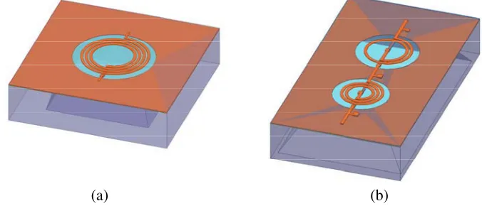
Figure 1 shows the designed structures of the suspended inductor and filter with patterned ground shields on low-resistivity (∼5 Ω·cm) silicon substrates. A cavity underneath the spiral coil is etched to reduce the silicon substrate losses. The excessive loss of the conventionally used silicon substrate can be avoided absolutely by the shielding layer which restricts the electromagnetic field to the half space above the silicon substrate.
(a) (b)
Figure 1. 3-D structures of the suspended (a) inductor and (b) filter with patterned ground shields.
Figure 2 illustrates the cross section at view of the IPD, which is composed of three metal layers and one BCB layer. In order to reduce ohmic loss, the layers Metal 2 and Metal 3 are made of thick copper by electroplating. The layer Metal 3 with a thickness of 8µm is used to form the spiral coil of the inductor. The underpass of the inductor and ground shields are implemented in Metal 2 with a thickness of 5µm. A thin layer (2000 ˚A) of Si3N4 between Metal 1 and Metal 2 is deposited for high density metal-insulator-metal (MIM) capacitors. The layer Metal 1 is made of magnetron sputtering Ti/Cu with a thickness of 4000 ˚A. Thick photosensitive BCB with a thickness of 12µm is used as the interlayer dielectric to planarize the bottom structures and reduce the capacitive coupling between the inductor and the MIM capacitor. The vertical interlayer connection via with the diameter from 25 to 100µm between Metal 2 and Metal 3 is formed by copper electroplating process and exposed by plasma mask-etching process after cure of the BCB layer. The line width and gap width of the designed inductor are 30 and 20µm, respectively.
Figure 2. Cross section of the integrated passive device technology in this study.
Full-wave electromagnetic (EM) simulation is used to study how the structure of PGS influences theQfactor and inductance of the suspended inductor. As shown in Figure 3, the suspended inductor with PGS has higherQfactor, especially in the range of 3–10 GHz, e.g., at 7 GHz, theQfactor increases 56%. The PGS lowers the inductance, indicating that the generation of eddy currents in the PGS is relatively low. Considering the trade-off between the inductance and theQfactor, our design has been optimized.
A low-insertion-loss LPF in 1.8 GHz DCS band (1.71–1.98 GHz) is designed to demonstrate the effect of the suspended structure with PGS. In this paper, we consider the following specifications for the filter: pass-band insertion loss of 0.4 dB, 3-dB cut-off frequency of 2.8 GHz, minimum attenuation of 25 dB and 35 dB at 3.6 GHz and 5.4 GHz respectively. According to the specifications, the 5th-order elliptic low pass filter circuit topology shown in Figure 4 is selected, due to its sharp cut-off characteristic. This configuration utilizes two parallel-tuned circuits where each condition of parallel resonance directly corresponds to a transmission zero. Thus, it would result in higher selectivity as required by the specifications.
According to the specifications and based on the design formula of elliptic low pass filters, the element values of the ideal circuit topology can be obtained [14]. In the circuit-level simulation, by using Agilent Advanced Design System (ADS) software, a much improved insertion loss is expected since there is no parasitic and loss for the ideal inductor and capacitor. After the simulation, an EM simulation is followed for the preliminary layout and is absolutely necessary in such designs since the close proximity of all these components can alter the performance of the filter significantly. In order to achieve the possible smallest form factor, the tank capacitor is placed inside the inner diameter of the tank inductor. According to the result of the EM simulation, the values and layout of the MIM capacitors are tuned until the targeted electrical performance is achieved. The component values for the LPF in DCS band after optimization are summarized in Table 1. As shown in Figure 5, a reasonable agreement between circuit and EM simulation is verified for the suspended filter with PGS, which is mostly attributed to the highQfactor of the inductors.
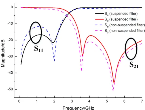
Figure 6 shows the simulation results of normal and ground-shielded suspended LPFs in DCS band. The proposed LPF has improved RF performance with very low insertion loss of only 0.33 dB at the pass band, and this value has been improved by a factor of more than 70% compared with non-suspended LPF.
Figure 4. Circuit diagram of the 1.8 GHz DCS LPF.
Figure 5. Comparing results of circuit simulation and EM simulation of suspended DCS LPF with PGS.
Table 1. Component values for the LPF in 1.8 GHz DCS band.
f0 (GHz) L1 (nH) L2 (nH) C1 (pF) C2 (pF) C3 (pF) C4 (pF) C5 (pF)
Figure 6. Comparison of the simulation results of both normal and proposed DCS LPF.
3. FABRICATION
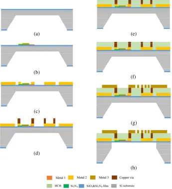
Suspended inductors and LPFs in the DCS band with PGS are fabricated on a 4-inch 100 silicon substrate with low resistivity (3–8 Ω·cm) and a thickness of 420µm. Utilizing wafer level integration and bulk Si etching technologies, the fabrication of the RF filters combines the process steps for both high-performance ground-shielded suspended inductors and suspended MIM capacitors. PECVD Si3N4 with a thickness of 2000 ˚A is used as the capacitor dielectric layer. The deposition of the insulator is carried out at a low temperature (300◦C) without post-annealing. After the fabrication, the measurement result is conducted as follows: the capacitance density is 330 pF/mm2, which is high enough for most of RF applications. Figure 7 illustrates the fabrication steps, which are detailed as follows.
(a) A 2µm thick silicon dioxide layer and a 0.2µm thick silicon nitride layer are formed on both sides of the wafer by thermal oxidation and low-pressure chemical vapor deposition (LPCVD) respectively. Windows for etching cavities are opened on the backside of the silicon dioxide and silicon nitride films. Afterwards, silicon anisotropic etching is carried out in 40 wt% potassium hydroxide (KOH) at 50◦C to form a 350µm deep cavity with an etching rate of about 10µm/h.
(b) By using magnetron sputtering, 50 nm thick titanium and 350 nm thick copper are sputtered on the top of the silicon nitride at the front side. Then, the Ti/Cu metal layer is patterned using the second photomask and etched through ion beam process to form the bottom plate of the capacitors. The photoresist can be removed by using the ultrasonic wet bench with acetone. By using PECVD, a silicon nitride layer of 200 nm thickness is deposited as the insulating dielectric layer of the MIM capacitors. Afterwards, the dielectric is patterned using the third photomask and etched using reactive ion etching. Then, another Ti/Cu seed layer (50 nm/200 nm) is sputtered and patterned as the top electrode of the capacitor. The measurement shows that the dielectric constant of this PECVD Si3N4 is found to be approximately 7.0.
(c) After Ti/Cu seed layer (50 nm/200 nm) is sputtered, a 7µm-thick photoresist (AZ9260) layer is coated and patterned. Then 5µm thick copper films are electroplated as the underpasses of the inductors and the ground shielding layer.
(d) To prepare the vertical interlayer connection via of 8µm thick copper, the same procedures as above are applied.
(e) The 12µm-thick BCB interlayer is coated by spinning after coating of Dow’s AP3000, followed by 90 seconds soft baking at 110◦C. The substrate is then soft cured in a box oven at 200◦C underN2. (f) To expose the connection via, a 5µm-thick photoresist (AZ9260) layer is coated and patterned.
The BCB above the connection via is removed by deep reactive ion etching (DRIE).
(a)
(b)
(c)
(d)
(e)
(f)
(g)
(h)
Figure 7. Flow chart of the fabrication process of the suspended filter with PGS.
(a) (b)
(c) (d)
interlayer connection via, this photoresist layer is experimentally confirmed to have an excellent development feature of the connection via by overdevelopment.
(h) The left 70µm-thick silicon under the backside cavities is etched by DRIE. The oxide membrane on the silicon wafer can protect the filters from etching.
Figures 8(a) and (b) show the top and back optical microscopy images of the fabricated suspended inductor with PGS. Due to the overdevelopment of the last photoresist layer, the line width and gap width of the fabricated inductor are 35 and 15µm, respectively. The top and back SEM images of the proposed LPF are shown in Figures 8(c) and (d), respectively. The LPF die in DCS band has a size of 2.5×1.45×0.45 mm3.
4. RESULTS AND DISCUSSION
The two-portS-parameters are measured with ANRITSU MS2038C vector network analyzer through on-wafer probing in ground-signal-ground (GSG) configuration. A short-open-load-thru (SOLT) calibration is applied to calibrate the measurement setup over the frequency range from 0.1 GHz to 10 GHz. The characteristic impedance of the measurement system is 50 Ω.
4.1. RF Characteristics Test of the Suspended Inductor with PGS
To characterize the RF performance of the proposed inductor, the element L1 is evaluated in the structure shown in Figure 8(c). The measuredS-parameters are first converted toY-parameters. Then, the parasitic parameters of the pad are removed by open de-embedding method using Eq. (1). Qfactor and inductance (L) are calculated using Eqs. (2) and (3).
Y = Ytotal−Yopen (1)
Q = −Im(Y11) Re(Y11)
(2)
L = Im(1/Y11)
2πf (3)
As shown in Figure 9(a), the measurement result ofQfactor of the proposed inductor is reasonably in accordance with the simulation in 0.1–2 GHz frequency range. However, at high frequency above 2 GHz, the measuredQfactor is higher than the simulated one. The difference between the simulation
(a) (b)
results and the tested data is mainly due to the following reasons. Firstly, the fabricated opening dimensions underneath the spirals are larger than the designed parameters, due to the over-etching of DRIE process. Therefore, the coupling between the inductor and the lossy silicon substrate can be reduced. Secondly, it is possible arise from the difference of the thickness of BCB from designed value due to the deviation of the parameter during processing. As the BCB layer thickness increases, the substrate loss decreases, resulting in higherQ-factor at high frequencies and more stable characteristic of the inductance. The fabricated inductor shows Qmax = 49 at 8.2 GHz, and its series inductance is 2.7 nH. As shown in Figure 9(b), the measured inductance shows good correlation with the simulated one with small discrepancies that may also be attributed to the process variations in fabrication, such as the metal thickness control during electroplating and the overdevelopment of the Metal 3 (Figure 8(a)).
4.2. RF Characteristics Test of the Suspended LPF in DCS Band with PGS
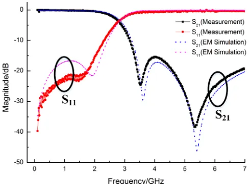
Figure 10 depicts the measured and simulated S-parameters at room temperature for the 0.1–7 GHz frequency range. The difference of insertion loss between measurement and simulation is relatively small in the pass band (1.71–1.98 GHz). The measured S-parameters demonstrate that the insertion loss at 1.8 GHz is 0.35 dB and the loss is less than 0.44 dB up to 1.98 GHz. The return loss is better than 15.5 dB in the pass band. Since the return loss is very sensitive to small layout features, it is difficult to predict the return loss very well. In our results, the return loss difference is within 4 dB in the pass band, indicating that the result is quite good. The second order (3.6 GHz) and third order (5.4 GHz) harmonic attenuations of 23 dB and 38 dB are achieved. In the pass band, the measured return loss shows higher than the simulated one. It is possible attributed to the decreased capacitances of the fabricated MIM capacitors. In the high-side stop band, the process variation is seen to have more impact on the frequency response shift. Multiple process variations may account for this frequency shift. The possible variations include:
1) The different width and space of the inductor would cause variation in inductance, due to the overdevelopment of the Metal 3.
2) The different width of capacitors and the thickness of the Si3N4 dielectric layer would cause the variation in capacitance.
3) A shift in the alignment between the top and bottom electrodes would affect the value of the capacitors and in turn cause a shift in the frequency.
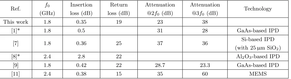
Table 2 summaries the filter performance and compares with prior arts of LPFs realized in other technologies using low-loss substrates similar to IPD, or MEMS technology. The proposed filter shows equivalent or better characteristics than those using other methods.
Table 2. Performance comparison with prior arts of LPFs.
Ref. f0
(GHz) Insertion loss (dB) Return loss (dB) Attenuation
@2f0 (dB)
Attenuation
@3f0 (dB) Technology
This work 1.8 0.35 19 23 38
[1]* 1.8 0.5 31 28 GaAs-based IPD
[7] 1.8 0.36 25 37 36 Si-based IPD
(with 25µm SiO2)
[8]* 2.4 2.8 22 Al2O3-based IPD
[9] 1.8 0.42 22 28.7 23.3 GaAs-based IPD
[11] 2.4 0.38 15 35 60 MEMS
* The data is not specified and is read from the figures of measurements.
5. CONCLUSIONS
A novel WL-integrated low-insertion-loss filter with suspended high-Q spiral inductor and patterned ground shields combining wafer level packaging and bulk Si etching technologies is proposed.
The design and fabrication of micromachined spiral inductors with suspended structure and PGS are presented, in order to minimize the substrate losses. The suspended structure supported by the thick BCB interlayer is robust and easy to realize by using a two-step back-etching process. With the well-developed substrate process and the PGS structure, high-Qinductors on low-resistivity silicon wafer are obtained, demonstrating a maximumQfactor of 49 of the 2.7 nH inductor and especially high
Q factors in the broadband frequency range from 1 GHz to 10 GHz. And a 1.8 GHz LPF in DCS band is designed and fabricated using these inductors. The fabricated LPF has the insertion loss of 0.35 dB at the pass band and the return loss of more than 15.5 dB, with the second harmonic rejection being 23 dB and the third harmonic rejection being 38 dB respectively. Furthermore, these inductors and filters provide the compatible capacity with the CMOS and WLP processes. It is concluded that, this suspending and ground shielding technologies for the high performance integrated passives will push the RF operating window of low-resistivity Si wafers well into 10 GHz and broaden the application area of IPDs.
ACKNOWLEDGMENT
The authors would like to thank SIMIT for the manufactory platform and package implementation.
REFERENCES
1. Liu, L., et al., “Compact harmonic filter design and fabrication using IPD technology,” IEEE Transactions on Components and Packaging Technologies, Vol. 30, No. 4, 556–562, 2007.
2. Zoschke, K., et al., “Wafer level processing of integrated passive components using polyimide or polybenzoxazole/copper multilayer technology,” IEEE Transactions on Advanced Packaging, Vol. 33, No. 2, 398–407, 2010.
3. Zoschke, K., et al., “Fabrication of application specific integrated passive devices using wafer level packaging technologies,”IEEE Transactions on Advanced Packaging, Vol. 30, No. 3, 359–368, 2007. 4. Han, M., G. Xu, and L. Luo, “High performance silicon-based inductors for RF integrated passive
devices,” Progress In Electromagnetics Research, Vol. 146, 181–186, 2014.
6. Kattelus, H., H. Ronkainen, and T. Riihisaari, “Passive integration process on standard and high resistivity silicon,” 1999 International Conference on High Density Packaging and MCMS, Proceedings, Vol. 3830, 194–199, 1999.
7. Kim, D. W., et al., “High performance RF passive integration on a Si smart substrate for wireless applications,” Etri Journal, Vol. 25, No. 2, 65–72, 2003.
8. Zoschke, K., et al., “Thin film integration of passives — Single components, filters, integrated passive devices,”54th Electronic Components&Technology Conference, Vols. 1 and 2, Proceedings, 294–301, 2004.
9. Pacheco, S., et al., “Compact low and high band harmonic filters using an integrated passives device (IPD) technology,” 2006 Topical Meeting on Silicon Monolithic Integrated Circuits in RF Systems, Digest of Papers, 346–349, 2006.
10. Wu, S.-M., C.-T. Kuo, and C.-H. Chen, “Very compact full differential bandpass filter with transformer integrated using integrated passive device technology,” Progress In Electromagnetics Research, Vol. 113, 251–267, 2011.
11. Wu, Z. Z., L. Gu, and X. X. Li, “Post-CMOS compatible micromachining technique for on-chip passive RF filter circuits,”IEEE Transactions on Components and Packaging Technologies, Vol. 32, No. 4, 759–765, 2009.
12. Yook, J. M., D. Kim, and J. C. Kim, “High-Qtrenched spiral inductors and low-loss low pass filters using through silicon via processes,”Japanese Journal of Applied Physics, Vol. 53, No. 4, 2014. 13. Yook, J. M., K. M. Kim, and Y. S. Kwon, “Suspended spiral inductor and band-pass filter on thick
anodized aluminum oxide,” IEEE Microwave and Wireless Components Letters, Vol. 19, No. 10, 620–622, 2009.