ABSTRACT
ZHU, QIANLAI. 7.2 kV Solid State Transformer Based on 15 kV SiC MOSFETs and A Novel Single Stage AC-AC Converter. (Under the direction of Dr. Alex Q. Huang.)
Solid state transformer (SST) is considered an emerging and disruptive power electronics
technology for medium voltage (MV) (2 kV-35 kV) applications including smart distribution system, traction transformer, ship power and renewable energy. SST concept is proposed that aims to replace conventional line frequency transformer (LFT), providing many advanced
features such as VAR compensation, voltage regulation, fault isolation, and DC connectivity. However, many challenges related to high voltage stress, efficiency, reliability, protection and
insulation must be addressed before the technology is ready for deployment.
Three-stage SST with ac-dc-dc-ac scheme is the most widely studied and adopted approach since it can achieve most of the smart features and owns best control flexibility. However, the
major disadvantage of this scheme is reduced efficiency due to multiple stages of power conversion. In addition, complex circuit and control configurations limit the system power
density. Direct AC-AC converter, named as direct AC-AC transformer (DACX), with one stage of power conversion is desirable in MV applications where higher efficiency is preferred
and only limited smart features are needed. In general, two major technical challenges in MV direct AC-AC converter needs to be addressed: (1) wide voltage range leads to a much more complex ZVS circumstance, (2) requirement in capacitance reduction to reduce unwanted
reactive power and MV capacitor’s size/weight.
capacitance, which helps improve system power density and reduce unwanted reactive power. Theoretical time domain analysis and fundamental harmonic approximation (FHA) are
conducted, providing design equations for switching frequency selection.
The 15 kV SiC MOSFETs developed by Wolfspeed enable simple and robust two-level DACX where the peak voltage stress is less than 12 kV. Chapter 3 revisited the
characterizations of 15 kV SiC MOSFETs including switching loss, Ron, thermal, output charge
and package. ZVS design of 15 kV SiC MOSFET is studied and analyzed under wide input
voltage condition (0 to 10 kV). Constant deadtime strategy is proposed, with which ZVS can be realized at most of high voltage range. Partial discharge occurs when input voltage is low. However, only neglectable associate switching loss will be generated if deadtime and Lm are
properly designed. Detailed analysis of ZVS behavior under wide range of voltage conditions and detailed calculation of associated loss from partial ZVS are presented.System parameters
including Lm and tdead are optimized based on tradeoff between turn on loss and conduction
loss.
Resonant capacitors are distributed on both sides of the transformer to minimize number
of MV MF SiC MOSFETs. Inherent cycle by cycle current-limit capability is achieved by paralleling diodes on low voltage (LV) resonant capacitors. The theoretical analysis and design
of DACX under overload and short circuit conditions are conducted. Equation for peak current calculation under short circuit is also provided. The calculation results show that the peak current is a function of the input voltage, resonant inductance and primary resonant
A full-scale and compact SSTs that converts 7.2 kV AC to 240 V AC is developed and tested from 600 kW to 12 kW. ZVS operation of the MV MOSFETs is verified from light load
to heavy load. This is the highest reported voltage rating for two-level based power converters without device series connection. The developed SST has achieved a peak efficiency of 97.8 %, which is a significant improvement from previously developed three stage SSTs. 15 kV
MOSFET is utilized to reach its full voltage, frequency and power potential of 10 kV, 100 kHz and 20 kW, respectively, in DACX applications. Short circuit is conducted under 3 kV peak
7.2 kV Solid State Transformer Based on 15 kV SiC MOSFETs and A Novel Single Stage AC-AC Converter
by Qianlai Zhu
A dissertation submitted to the Graduate Faculty of North Carolina State University
in partial fulfillment of the requirements for the degree of
Doctor of Philosophy
Electrical Engineering
Raleigh, North Carolina 2018
APPROVED BY:
_______________________________ _______________________________ Dr. Alex Q. Huang Dr. Xiangwu Zhang
Committee Chair
DEDICATION To my parents
BIOGRAPHY
Qianlai Zhu was born in Wenzhou, China, in 1988. He received the B.S. degree in electrical
engineering from Zhejiang University, Hangzhou, China, in 2010. From 2010 to 2013, he was an Electrical Engineer with the Delta Electronics Co., Shanghai China, where he was engaged in design and implementation of server power supply and automotive onboard charger.
Currently he is pursuing the Ph.D. degree in the Department of Electronic and Electrical Engineering at the North Carolina State University. His research interests include Solid State
ACKNOWLEDGMENTS
I would like to express my sincere thanks to my advisor, Dr. Alex Q. Huang, for his
patience with me. Thank him for his mentorship, encouragement and support during the past five years here at FREEDM system center, NC state university. I especially appreciate and respect Dr. Huang for his broad vision and insight understanding of technology, as well as his
greatly personalities.
I would like to express my gratitude to Dr. Wensong Yu, for his guidance and support in
my research. I would thank my committee members Dr. Srdjan Lukic and Dr. Xiangwu Zhang, for their suggestions to improve this dissertation.
Special thanks to faculties and staffs in the FREEDM system. I would like to thank Dr.
Iqbal Husain, Mrs. Karen Autry, Mr. Hulgize Kassa and Mrs. Audrey Callahan for their help and support.
I am very grateful to SST (Solid State Transformer) team members including Dr. Gangyao Wang, Dr. Fei Wang, Dr. Xu She, Dr. Xijun Ni, Dr. Li Wang, Dr. Dong Chen, Dr. Sheng Zong, Mr. Yang Lei, Mrs. Kristen Booth, Mr. Liqi Zhang, Mr. Soumik Sen and many others who
have worked on the SST project.
I would like to thank friends and colleagues in FREEDM system center including Dr. Qi
Tian, Dr. Ryan Yu, Dr. Kai Tan, Mr. Zhiping Chen, Dr. Yizhe Xu, Dr. Rui Gao, Dr. Suxuan Guo, Dr. Fei Xue, Dr. Xiaoqing Song, Dr. Chang Peng, Mr. Qingyun Huang, Dr. Xiangqi Zhu, Mr. Yue Shi, Mr. Jian Lu, Mrs. Lisa Sun, Mr. Haotao Ke, Mr. Xin Zhao, Mr. Tianxiang Chen,
My heartfelt gratitude goes to my parents Yingqi Zhu and Xiaoling Wang for their love and support. Thanks to my sisters Congrong Zhu, Yanqun Zhu and Jun Zhu for their help and
support during my research.
Lastly, I would like to express my gratitude whole heartedly to my beloved girlfriend Yuling Zhao, who have sacrificed too much to support me. Your love and encouragement make
TABLE OF CONTENTS
Chapter 1. Introduction ... 1
1.1 Introduction to Solid State Transformer Concept ... 1
1.2 Literature Review ... 2
1.2.1 Topology State of the Art ... 4
1.2.2 Modular and Two-level Approach ... 6
1.3 Research Scope and Objectives... 8
1.4 Dissertation Outline... 10
Chapter 2. Current Fed Series Resonant Converter for Direct AC-AC Application ... 12
2.1 Introduction of Direct AC-AC Converter ... 12
2.1.1 Review on ZVS Topologies for Direct AC-AC Converter ... 14
2.1.2 Review on Capacitance Reduction Methods ... 16
2.2 Proposed CFSRC ... 23
2.2.1 Proposed Current Fed Series Resonant Converter (CFSRC) ... 23
2.3 Proposed Direct AC-AC Converter... 25
2.3.1 Operation Principle ... 28
2.3.2 Time Domain Analysis ... 30
2.3.3 Fundamental Harmonic Approximation ... 34
2.3.4 Voltage Gain Investigation ... 43
2.3.5 Extension Application of ICF Cell ... 45
2.4 Conclusion ... 46
Chapter 3. 15 kV SiC MOSFETs Revisit and ZVS Design Over Wide Voltage Range .... 47
3.1 Introduction ... 47
3.2 15kV SiC MOSFET Revisit ... 50
3.2.1 On-State Resistance Model ... 51
3.2.2 Device Packaging Consideration ... 53
3.2.3 Switching Loss Model ... 56
3.2.4 Thermal Consideration... 62
3.3 ZVS Design Based on 15 kV SiC MOSFET ... 62
3.4.1 Conduction Loss ... 68
3.4.2 Transformer Loss Calculation... 70
Figure 3-21 Flux density vs. time ... 72
3.5 Device Switching Frequency and Power Utilization ... 73
3.6 Conclusion ... 75
Chapter 4. Over-load and Short Circuit Current Limiting of the Proposed CFSRC ... 76
4.1 Introduction ... 76
4.1.1 Introduction to Fault Current Limitation in MV Applications ... 76
4.1.2 SRC Current Limit Review ... 77
4.2 Proposed CFSRC with Inherent Current Limitation ... 79
4.3 Circuit Configuration ... 79
4.3.1 Operation Principle under Over Load Condition ... 83
4.3.2 Operation Principle under Short Circuit Condition ... 87
4.4 Resonant Tank Design Consideration ... 91
4.5 Conclusion ... 92
Chapter 5. Hardware Development and Experimental Verification ... 93
5.1 Hardware Development... 93
5.1.1 Delta-sigma Based Fiber Optical High Voltage Sensor ... 98
5.2 Experimental Verification ... 101
5.2.1 Steady State Test ... 101
5.2.2 Short Circuit Experimental Verification ... 106
5.3 Conclusion ... 108
Chapter 6. Conclusion and Future Work ... 109
6.1 Contributions Summary ... 109
6.2 Future Work ... 111
LIST OF TABLES
Table 1-1 Summary of Previous Developed Prototypes ... 3
Table 2-1 Electrolyte and Film Capacitor Comparison Summary... 19
Table 2-2 Current Zero Crossing Equivalent Frequency ... 45
LIST OF FIGURES
Figure 1-1 SSTs application Areas ... 1
Figure 1-2 MV prototypes with key parameters by leading research groups ... 3
Figure 1-3 Topology classification ... 6
Figure 2-1 Direct AC-AC Operating Principle ... 12
Figure 2-2 Dual Active Bridge based AC-AC converter circuit used in [30] ... 14
Figure 2-3 SST with direct AC-AC isolated front end based on SRC circuit [11] ... 15
Figure 2-4 Circuit and Equivalent Small Signal Model of Conventional SRC ... 18
Figure 2-5 Operation waveform of VFSRC at resonant frequency. ... 18
Figure 2-6 Rectifier circuit with ripple eliminator to reduce capacitance ... 21
Figure 2-7 SRC circuit with LC filter on output side ... 22
Figure 2-8 Single switch ICF cell ... 23
Figure 2-9 Half bridge ICF cell ... 24
Figure 2-10 Circuit and Equivalent Small Signal Model of Current Source SRC ... 25
Figure 2-11 Proposed Configuration 1 ... 26
Figure 2-12 Proposed Configuration 2 ... 27
Figure 2-13 Proposed Configuration 3 ... 27
Figure 2-14 Circuit of Current Source SRC ... 28
Figure 2-15 Detailed Operation Waveforms of Current Source SRC ... 29
Figure 2-16 Equivalent circuit of the CFSRC... 30
Figure 2-19 Current approximation. ... 35
Figure 2-20 Secondary side resonant capacitor voltage ... 36
Figure 2-21 Vac and its three elements composition. ... 38
Figure 2-22 Fundamental components approximation. ... 40
Figure 2-23 Equivalent frequency domain circuit. ... 41
Figure 2-24 AC Equivalent circuit, neglecting Lm ... 41
Figure 2-25 AC Equivalent circuit including Lm ... 43
Figure 2-26 A family of circuit based on ICF cell ... 44
Figure 3-1 6500 V / 600 A IGBT from ABB... 47
Figure 3-2 I-V curve comparison of 15-kV SiC P-GTO, IGBT, and MOSFET at 25 C and 125 C. [59] ... 48
Figure 3-3 15 kV SiC MOSFET ... 50
Figure 3-4 On-state resistance of the 15 kV SiC MOSFET modules [14] ... 51
Figure 3-5 10 kV/120 A SiC MOSFET Module [10] ... 52
Figure 3-6 15 kV SiC MOSFET packaging types ... 53
Figure 3-7 Turn on and turn off waveforms under 8 kV/ 8 A condition ... 57
Figure 3-8 Output charge of 15 kV SiC MOSFET modules ... 58
Figure 3-9 The Eon and Eoff of the 15 kV SiC MOSFET [52] ... 59
Figure 3-10 The MV devices’ Voltage*Frequency capability ... 61
Figure 3-11 Typical operation waveforms ... 63
Figure 3-12 Required and proposed deadtime versus input voltage ... 64
Figure 3-14 Partial discharge theory. ... 65
Figure 3-15 Residual Q and voltage versus input voltage. ... 66
Figure 3-16 Turn on loss vs deadtime at 40 kHz. ... 67
Figure 3-17 Current waveform of SRC ... 68
Figure 3-18 Total CFSRC semiconductor loss versus magnetizing inductance and deadtime. ... 70
Figure 3-19 Transformer ... 71
Figure 3-20 Core loss vs. flux density at 100°C ... 72
Figure 3-21 Flux density vs. time ... 72
Figure 3-22 15kV SiC MOSFET junction temperature versus power with different fs and ... 74
Figure 4-1 VFSRC with split resonant cap and diodes at output side ... 78
Figure 4-2 VFSRC with split resonant cap and diodes at input side ... 78
Figure 4-3 Proposed CFSRC with split resonant cap on both side and clamping diodes at output side ... 80
Figure 4-4 Operation waveforms under over load condition ... 81
Figure 4-5 Operation waveforms under over load condition ... 82
Figure 4-6 Operation waveforms under short circuit condition. ... 88
Figure 4-7 Equivalent circuit of the CFSRC during t1-t2 at short circuit. ... 89
Figure 4-8 Peak current versus k at different peak voltage conditions. ... 91
Figure 5-1 Control board of 7.2kV TLSS SST. ... 96
Figure 5-4 Voltage Sensor: Comerical 4.2kVdc voltage sensor ($560) versus proposed fiber
optical sensor (>10kV) ($50) inductors ... 99
Figure 5-5 Source signal vs sensed signal by high proposed v1oltage sensor... 100
Figure 5-6 Hardware structure of 7.2kV TLSS SST... 100
Figure 5-7 Steady state operation waveforms ... 101
Figure 5-8 Steady state operation waveforms ... 102
Figure 5-9 Steady operation waveforms. ... 103
Figure 5-10 Test efficiency result and loss breakdown ... 105
Figure 5-11 Short circuit waveforms at 3 kV peak input voltage - 1 ... 106
Chapter 1.
Introduction
1.1 Introduction to Solid State Transformer Concept
In recent years, there has been a growing interest in replacing the traditional bulky low frequency (LF) transformers (LFT) with solid state transformer (SST) in medium voltage
(MV) (2 kV-35 kV) applications. Due to its benefits in size and weight reductions, as well as a number of smart functionalities, SST concept is increasingly investigated and implemented in many applications such as smart grid, traction drive and renewable energy systems shown
in Figure 1-1 [1]-[4]. SSTs play crucial role to connect different loads, AC or DC systems and offer galvanic isolation, voltage regulation and fault current limitation.
Magnetic transformer’s area product is inversely proportional to its operation frequency. Increasing frequency enables significant reduction in transformer volume and weight. The
basic idea is use semiconductor power devices to generate medium frequency (MF) (several kHz to tens of kHz) voltages, step up/down them through MF transformer, and reshape them back to LF voltages. To accomplish this, semiconductor devices, gate drivers, inductors,
capacitors and control system are needed to form a compact system. With the help of power electronics technology, many attractive features that is not available in LFTs, including VAR
compensations, voltage regulation, fault isolation and DC link, can be realized in SSTs [1]-[4]. Power electronics technology has been well established in low voltage (LV) applications with voltage that is less than 1 kV. However, the application of this technology in MV
applications is still far from mature and many challenges need to be solved before commercializing this new concept. Current researches mainly focus on semiconductor device,
topology and control design.
1.2 Literature Review
Different power conversion topologies and applications of SST family have been
implemented and presented [1]-[12]. The primary research targets are to achieve high efficiency, reliability, functionality and power density, while maintain low cost.
Figure 1-2 MV prototypes with key parameters by leading research groups
The qualitative comparison for medium voltage prototypes are summarized in Table 1-1. The table shows that these developed prototypes offers attractive features such as Var
compensation, fault isolation and so on.
On the other hand, these accomplished works still cannot match conventional LFT in performance of efficiency, cost and life time performance at current stage.
1.2.1 Topology State of the Art
So far, the literatures on SST design show a variety of technical approaches. Five different
power conversion topologies of the SST family have been implemented and presented in MV applications as depicted in Figure 1-3 [6]-[15].
Type D is the most widely studied and adopted approach since it can achieve most of the
smart features such as VAR compensation, voltage regulation, fault isolation, and DC connectivity [3]. However, the major drawbacks of Type D are reduced efficiency due to
multiple stages power conversion and reduced reliability due to complex hardware configuration and control [7], [15]. Furthermore, previous research has shown that the input AC-DC stage normally operates under hard switching condition, the switching frequency is
greatly limited by huge amount of switching loss, which in turn limits the power density. Current built SSTs based on this topology report overall system efficiency lower than 95%.
Types B and C are topologies that adopt two-stage configurations, which can achieve higher efficiency compared to Type D due to one less stage of power conversion. However, DC voltage needs to be generated inside the system, which create some obstacles in design.
voltage gain capability [16], [17], which requires complex control and PWM modulation. In Type C topology, MV AC-DC stage still exists, which greatly limits the switching frequency
and efficiency performance. The isolated DC-AC stage also requires specific control or PWM modulation to realize soft switching and wide voltage gain [18], [19].
Type E is proposed in paper [20] and is named as isolated front end (IFE) approach. Which
is suitable for MV AC to LV DC power supply applications. The first stage directly converts MV AC voltage to LV half sinusoidal voltage. This stage is designed at an optimized point to
achieve high efficiency and simple control configuration. The grid current power factor correction and output voltage regulation is carried out by a second, non isolated conversion stage on the LV side.
Type A topology, named as direct AC-AC transformer (DACX) in this dissertation, is an attractive approach since only one stage of power conversion is needed. This approach directly
converts MV AC voltage to LV ac voltage without converting to DC voltage. There are two types of Type A topologies. Type A-1 use four-quadrant switches on both sides of the transformer to directly converting power. Type A-2 is actually an extension of Type A-1, in
which bidirectional AC voltage is rectified and unfolded by input and output LF unfolding bridges. The HF stage of Type A-2 only sees unidirectional voltage, thus simple switches can
be used and HF switches numbers can be reduced to half. The system configuration of Type A is much simplified and MV MF power devices numbers is also minimized compared to previous topologies, which potentially enables better efficiency, higher reliability and is more
Although several studies have indicated that Type A topology offers best efficiency performance, little attention has given to this topology in MV applications due to its lacking functionalities and design challenges.
1.2.2 Modular and Two-level Approach
The most popular distribution voltage in the United States is the 15 kV class and the most
common 15 kV voltage is 12. 47 kV, which has a phase voltage of 7.2 kV. One grand challenge for the SST is to achieve MV input voltage such as 7.2 kVac in single phase smart grid
MVAC Type A-1
LVAC
Type B
Type C
Type D
Type E
MVAC LVDC
MVAC
MVAC
MVAC
LVDC
MVDC
LVRAC
LVAC
LVAC
LVDC LVAC
LVDC
MF
MF MF
MF MF
MF
MF
MF
MF
MF
Type A-2
MVAC LF MVHAC MF LVHAC LF LVAC
application. No commercial power devices are currently available to handle the associated peak voltage stress.
Modular multilevel configurations are widely used to address this issue in which low voltage converters or devices are connected in series to share the voltage and power [5]-[13].
Modular approach solves the voltage or current stress problems, especially enables low
voltage devices to accomplish power conversion in medium voltage applications. However, it also brings many problems. For example, to avoid power and voltage balancing problems,
additional balancing circuits and control strategies are needed [15]. Furthermore, the resulting SST is typically very complex due to the complex system configuration and control schemes, numerous gate drivers and isolated power supplies. System reliability is low if redundancy is
not carefully considered.
Due to the significantly increased bandgap and peak electric field stress, new MV power
devices based on SiC material with significant higher voltage rating, such as the 15 kV SiC MOSFETs and 15 kV SiC IGBT, have been developed and demonstrated [21]-[27]. They can enable simple and robust two-level SST in 7.2 kV applications where the peak voltage stress
is less than 12 kV. Compared to IGBT, the SiC MOSFET shows a much lower switching loss. This overall lower switching loss and ZVS capability enables higher switching frequency in
The 15 kV SiC MOSFET developed by Cree allows simple and robust two level SST in 7.2 kV applications where the peak voltage stress is less than 12 kV. But research on this
devices in continuous MV operation is still not enough.
1.3 Research Scope and Objectives
Based on previous statements, a two level, Direct AC-AC converter, offers perhaps the
best performance in efficiency and reliability. The target of this dissertation is to design and implement a two level DACX based on the 15 kV SiC MOSFETs, achieving good performance
in terms of efficiency, switching frequency and functionality.
Although many researches have been done on type A SSTs, there are still many areas needs more researches and improvement. Several practical challenges arise when introduce two level
Type A topology into MV applications.
Topology investigation: Zero voltage switching (ZVS) is the key to achieve high switching
frequency. Hard switching in MV applications will significantly limit the switching frequency due to the energy loss from device’s output charge [28]. It is crucial to select a proper topology that helps realize ZVS in MV DACX applications. In direct AC-AC converter, the input
voltage varies from zero to peak AC voltage every LF cycle. The changing of device voltage stress, together with the nonlinear output charge of MOSFET, make it difficult to achieve ZVS
operation. In addition, capacitance in the direct AC-AC converter will result in unwanted reactive power, which will affect the power factor. On the other hand, film capacitors are preferred in MV applications for their longer lifetime, higher ripple current capability,
energy density of film capacitors normally results in large volume. The high voltage insulation also leads to larger volume and weight, which limits the system power density. There is a
strong desire for a topology that can help reduce required system capacitance.
15 kV SiC MOSFET investigation and utilization: Previous studies have characterized this device thoroughly and have proven the voltage blocking capability of this device up to 12 kV
[22]. However, the achieved continuous operation of this device is still lower than 6 kV [14], and the highest achieved switching frequency is 40 kHz with ZVS operation [14]. The main
challenges in reaching higher operation voltage include ZVS operation range, poor and/or unproven reliability of the prototype device and its associated package. Much better auxiliary circuits such as driving circuit and auxiliary power supplies must also be designed to handle
the high isolation voltage as well as high common mode voltage range. More research works need to be done to utilize this device to its full voltage, frequency and power potential.
Furthermore, in direct AC-AC applications, designers must also face a new and significant challenge in realizing ZVS over a wide input voltage range (from 0 V-10 kV). More investigation and researches are required to properly implement this device in MV DACX
applications.
Current limit capability investigation: The ability to protect the power system from load
disturbances is another function that distinguishes SSTs from the conventional low frequency transformer. Fault current limiting capability is a very desired property in MV applications. It is important to design and investigate the current limiting capability of DACX when overload
The primary objective of this research work is to design and implement a two level direct AC-AC SST for 7.2 kV application with high efficiency performance and power density. This
dissertation offers comprehensive design guidelines for MV DACX design in terms of topology investigation, ZVS design and current limiting design. Offering guidelines for studying and utilizing SiC MOSFETs devices to its full switching frequency, voltage and
power potential in MV DACX.
1.4 Dissertation Outline
This dissertation is organized into 6 chapters.
Chapter 2 proposed a novel current fed series resonant converter (CFSRC) for direct AC-AC applications, which not only able to achieve ZVS operation across wide input voltage and
load range, but also minimize the total capacitance required in the system. The detailed theoretical analysis and operation principle of proposed circuit are conducted based on time
domain analysis and fundamental harmonic approximation (FHA). Equations on current zero crossing, gain property are provided for design reference.
Chapter 3 first revisits the 15 kV SiC MOSFET’s characteristics. Providing comprehensive design guidelines on utilizing the device to its full switching frequency and power potential in MV DACX in terms of ZVS implementation, loss optimization, thermal management and
device utilization
Chapter 4 is devoted to the analysis and design of the proposed circuit under over load conditions and short circuit condition. Design equation for peak current under short circuit is
Chapter 5 elaborated the system hardware development. Experiments for steady state operation are conducted under 7.2 kV conditions to verify the circuit operation principle. Test
result under light load and heavy load conducted to verify ZVS operation. Short circuit is conducted at 3 kV peak voltage to verify the overload current limiting capability.
Chapter 2.
Current Fed Series Resonant Converter for
Direct AC-AC Application
2.1 Introduction of Direct AC-AC Converter
The most adopted type D SSTs offers many functionalities such as Var compensation on
the input side or a 400V DC port for other purpose connection. However, three stages of power conversion limits its efficiency performance. Direct AC-AC converter only has one stage of power conversion, which is desirable in MV applications where higher efficiency is preferred
and full smart features are not needed.
Direct AC-AC converter with galvanic isolation is first proposed by William McMurray in
1970. Detail circuit is shown in Figure 2-1, in which four-quadrat thyristors are used to develop
P
2P
1P
4P
3V
inS1
S
2S3
S
4V
oan electronic transformer [29]. Low frequency input AC voltage is directly chopped into high frequency waveform with semiconductor devices. A high frequency transformer then converts
this high frequency waveform to the secondary side. Semiconductor devices on the secondary side will reshape the high frequency waveform back into low frequency AC voltage. Four quadrant switches are used, operating in complementary mode with 50% duty-cycle in this
application. This topology can be recognized as hard switching dual active bridge circuit. Power and voltage is controlled based on the phase shift between primary bridge and secondary
bridge. All devices in this topology operate under hard switching conditions.
In direct AC-AC configurations, ac voltage is directly processed into high frequency voltage, so there is no need of DC capacitors in the system. The control and design of the high
frequency isolation stage is critical. The overall system configuration is very simple, which contributes to better reliability. Single stage of power conversion also leads to higher
efficiency.
In recent years, many works have been done to introduce direct AC-AC converter into MV applications, most of which are designed based on modular structure. These research works
mainly focus on topology and control design. To the author’s best knowledge, none of previous finished research work on DACX has experimental results on voltage over 2 kV.
2.1.1 Review on ZVS Topologies for Direct AC-AC Converter
The first challenge comes from wide input voltage range, which requires the selected
topology to realize ZVS operation over wide range of voltage. This is drastically different from DC-DC converter. At 7.2 kV input condition, semiconductor devices need to process voltage that is changing from 0 V to 10 kV every line frequency cycle. The selected topology
need to obtain zero voltage switching (ZVS) across extremely wide voltage and load conditions.
Great efforts have been devoted to address the ZVS challenges in DACX. Paper [30] proposed a direct AC-AC converter based on dual active bridge (DAB) topology for MV application. Detail circuit is shown in Figure 2-2, in which four-quarter devices are adopted.
Dual active bridge (DAB) circuit is a popular topology in DC-DC applications with relative good ZVS capability and controllability. However, when applied it in direct AC-AC
applications, this circuit shows some limitations. This circuit has drawbacks of limited ZVS range. ZVS might be lost at light load or low input voltage conditions. In addition, the turn off current is high in this circuit, especially when load is heavy, which might contribute to higher
switching loss and limit converter’s efficiency performance. Additional auxiliary circuit or complex control scheme can be used to extend the ZVS range in DAB [31],[32], but may lead
to higher conduction loss. Due to the concern of complex ZVS circumstance, DAB topology is not adopted in this dissertation’s research.
Series resonant converter (SRC) is another popular circuit that is widely adopted in DC-DC applications. ZVS of this topology is independent of load conditions, which means that if
ZVS is achieved at one load point, it can be achieved across entire load range. When applied SRC in DACX, more research works are needed to investigate the ZVS behavior of SRC over wide range of input voltage. An Isolated Front End (IFE) SST based on series resonant (SRC)
topology is proposed in [33] and the detail circuit is shown in Figure 2-3. The circuit is a modular based direct AC-AC converter that converts AC input voltage to a half sinusoidal
voltage. SRC circuit is used in the isolated front stage to achieve ZVS operation of the primary switches under wide input voltage range. This paper uses a modular based input series output parallel structure with each stage’s operating of 900 V.
From previous statements, SRC circuit is more attractive in DACX application for its non-load dependent ZVS capability. However, besides ZVS operation, other challenges need to be
addressed before applying SRC circuit in direct AC-AC converter.
2.1.2 Review on Capacitance Reduction Methods
The second challenge for DACX is that a proper topology is needed to reduce the total capacitance in the system.
There is no DC voltage inside DACX, thus no DC capacitor is needed. Capacitance inside system will lead to unwanted reactive power and this reactive power might affect input power
capacitance will result in large reactive power. For example, if the applied input voltage is 7.2 kV, a capacitance value of 50 nF will generate 1 kW reactive power.
𝑄 = 𝑉𝑎𝑐
2
𝑋𝑐 = 𝑉𝑎𝑐
2𝜔
𝑙𝑖𝑛𝑒𝐶𝑡𝑜𝑡𝑎𝑙 2.1
LLC type SRC is selected as the topology in this research work for its ZVS capability.
However, conventional SRC circuit normally has large capacitance, which is not applicable in our application due to the reactive power consideration. More investigation into SRC circuit is
needed.
Typical conventional SRC circuit for DC-DC application is shown in Figure 2-4. Both the input side and output side of the circuit are large DC capacitors. These capacitors are used to
carry and filter the large ripple current from the resonant tank. This is named as voltage fed series resonant converter (VFSRC) since both side of the converter can be regarded as voltage
sources. The AC equivalent circuit model based on FHA analysis is shown in Figure 2-4, which indicates that the resonant tank is powered by two voltage sources. The equivalent resonant frequency of the circuit is derived as
𝑓𝑟 = 1
2𝜋√𝐿𝑟𝐶𝑟
2.2
When the circuit’s switching frequency is selected at this resonant frequency, the system gain equals to 1 and this gain is independent of load conditions. Switching frequency is
normally chosen around the resonant frequency for high efficiency performance.
Typical operation waveforms of VFSRC at its resonant frequency are shown in Figure 2-5. Turn off current of VFSRC is list in (2.4), in which the turn off current is the function of input voltage, switching frequency and magnetizing current. As long as the input voltage, Lm
and switching frequency are constant, this turn off current is constant and is independent of load conditions. This property is the major advantage of SRC circuit over DAB circuit.
P2 P1
Crp2
S1
S2 ip
Co Crp1
n:1
Crs1
Lm
im Ro
is
Lrs Lrp
Crs2
Cr_eq Lr_eq ir
VMV nVLV
Figure 2-4 Circuit and Equivalent Small Signal Model of Conventional SRC
Figure 2-5 Operation waveform of VFSRC at resonant frequency.
V
gs1V
gs2I
LrI
Lmt
dT
s𝐼𝐿𝑚(𝑉𝑑𝑠) =V𝑑𝑠𝑇𝑠
8𝐿𝑚 2.4
ZVS capability over wide load range makes SRC circuit an attractive topology. However,
for conventional VFSRC, large capacitance is normally required for ripple current filtering, especially in high power applications such as the low voltage (LV) side of MV converter. In
LV DC-DC conditions, electrolytic capacitors are normally chosen to absorbing rippling current and provide DC voltage due to their 3 times higher energy density than film capacitors. Thus, VFSRC circuit is not a good choice in DACX.
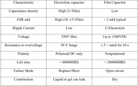
Table 2-1 Electrolyte and Film Capacitor Comparison Summary Characteristic Electrolyte capacitor Film Capacitor
Capacitance density High (3×Film) Low
ESR mΩ High (10~15×Film) < 2 mΩ typical
Ripple Current Low 2×Electrolyte
Voltage 550V Max Up to 1500VDC
Resistance to overvoltage 50 V Surge 1.5 × rated for 10 s
Polarity Polarized DC only Nonpolarized
Life time < 80000HRS > 200000HRS
Failure Mode Rupture/Short Open circuit
When it comes to the medium voltage, case is slightly different. The much higher voltage level also results in large impact on the capacitors that can be used.
Table 2-1 provides the comparison summary between electrolytic capacitor and film capacitor. In DACX applications, electrolytic capacitor is not applicable since electrolytic capacitor can only handles polarized DC voltage. In addition, electrolytic capacitors normally
have limited lifetime (less than 80000HRS), low voltage stress and low ripple current capability. Thus, for MV DACX applications, electrolyte capacitor is not applicable.
In contrast, film capacitor offers much longer lifetime (over 100000HRS) and 2 times higher ripple current density, which are very attractive. Furthermore, film capacitor owns very low ESR, much higher voltage rating and has open circuit failure mode, which make it very
suitable for MV applications. The drawback of film capacitor is its low energy density, which is typical one third of electrolyte capacitor. Low energy density result in larger volume and
weight when comparing to electrolyte capacitor with same value. As voltage rating increases, film capacitor’s volume and weight also increase dramatically due to the high voltage insulation requirement. Capacitor’s volume has become an important limitation that limit the MV converter power density.
On effective way to solve this issue is reducing the required capacitance inside system.
This idea is coordinate with previous requirement that trying to limit system reactive power. Reducing the required system capacitance enables an all film capacitor MV DACX, which helps improve system lifetime performance and power density.
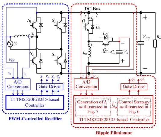
Paper [35] introduced a ripple eliminator circuit into rectifier circuit to reduce system DC capacitance. The detail circuit is shown in Figure 2-6. Ripple current is transferred into
auxiliary capacitor during operation, which helps reduce the required DC capacitance. However, this method requires additional switches, passive components and control circuits, which is not practical in MV applications.
Series resonant converter with inductive output filter or LC output filter are proposed in
[36], [37] to reduce the ripple current of the output capacitor, which helps reduce output capacitance. Detail circuit and inductor current are provided in Figure 2-8. This method is
useful in capacitance reduction since the added inductor helps reduce current ripple that flows into capacitors. However, it brings new issue. Since full bridge is used in this circuit, the
resonant tank current is directly related to the output inductor current. As can be seen from the inductor waveform, the current inside the resonant tank is clamped by output current during operation. This square current is much different from the original desired sinusoidal like
current in conventional SRC circuit. The ZVS properties of SRC is greatly affected by the added input and output inductor.
ILr
Ts
Figure 2-7 SRC circuit with LC filter on output side
P2
P1 S1
S3 Lr ir vMV Lg Co n:1 Lm Lo
vLV
Previous research shows that adding inductor helps reduce current ripple, which helps reduce capacitance. At the same time, the resonant current inside resonant tank should not be affected by the added inductor. Paper [38] proposed an input current fed (ICF) cell as shown
in Figure 2-8, which is named as input current fed cell. The capacitor Cr in this cell not only
works as a resonant capacitor to achieve resonant current inside resonant tank, but also works
as a decoupling capacitor that helps decouple the input DC current and resonant current. With this ICF cell, ZVS on and ZCS off for switches can be realized and system capacitance can be minimized.
2.2 Proposed CFSRC
2.2.1 Proposed Current Fed Series Resonant Converter (CFSRC)
In this dissertation, a symmetric half bridge Current-Fed SRC (CFSRC) based on half bridge ICF cell is proposed for MV direct AC-AC application. Detail circuit is shown in Figure
2-9. This approach shows many benefits when applied in DACX.
Firstly, this approach helps minimize the total capacitance in the system. Since the proposed SRC is based on current fed, the input and output side current ripple is filtered with inductors,
thus only minimum value of capacitance is needed in the system. Reactive power generated by capacitance in AC system is also minimized. Film capacitor can be used instead of aluminum
capacitors for longer life cycle performance while high power density is still achievable.
Secondarily, both sides of the circuit adopt half bridge structure with split capacitors forming a bridge leg. These capacitors help decoupling the MF resonant current inside the resonant tank and LF current on input/output side. Therefore, sinusoidal shape of current
waveform is still achieved in resonant tank, ZVS conditions is similar to conventional VFSRC and can be achieved across wide voltage and load range.
P
2P
1C
rp2i
pC
rp1L
ini
LinL
rpFirst harmonic approximation (FHA) is a powerful tool to analyze resonant converters near resonant frequency [39], [40].
Figure 2-10 shows the circuit and its AC equivalent circuit. The resonant tank can be regarded as powered by input and output current sources.
2.3 Proposed Direct AC-AC Converter
Based on the proposed CFSRC circuit, detail DACX system configuration can be derived. Figure 2-11 shows the proposed circuit configuration 1, which is based on Type A-1
structure. Four-quadrant switching cells are used in this case. Bidirectional power flow is realizable in this configuration. Half bridge structure is adopted to reduce the numbers of MF
MV SiC MOSFETs. There are four MF MV SiC MOSFETs in total in the proposed system.
P
2P
1C
rp2S
1S
2i
pC
oC
rp1n:1
C
rs2C
rs1L
mL
oi
mR
oi
sL
rsv
tpi
LoL
ini
LinL
rpC
rp1C
rs1_eqI
o/n
L
r_eqI
ini
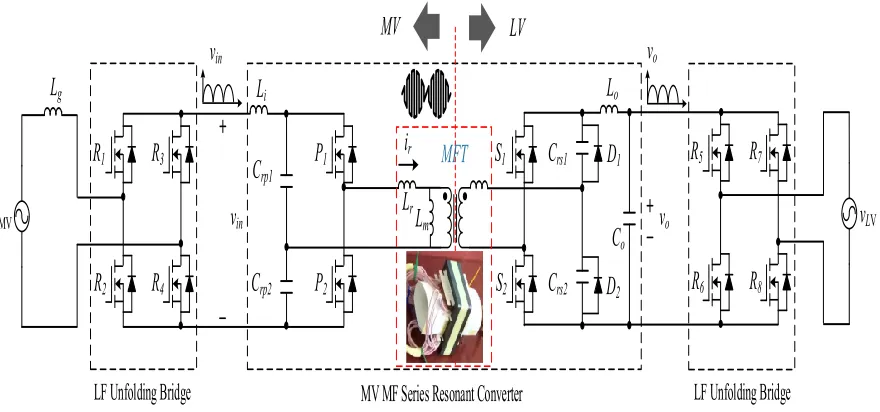
rTo further reduce the number of MF MV SiC MOSFETs, configuration 2 based on Type A-2 is proposed Figure A-2-1A-2. This circuit consists of a MV LF folding stage that converts LF MV
ac voltage to half sinusoidal voltage. The second stage adopts MF series resonant converter to convert half sinusoidal MV to half sinusoidal LV. The final stage is an unfolding stage that converts the LV half sinusoidal voltage back into LF AC voltage. The input and output stages
operate at line frequency, thus there is only conduction loss exist in these two stages. The MF MV stage only need to deal with unidirectional voltage, so simple MOSFETs can be used in
the MF stage. The system contains a minimum number of 15 kV SiC MOSFETs- P1 and P2.
P2 P1
Crp2
S1
S3
Lr
ir
vMV
Lg
Co
Crp1
n:1
Crs2
Crs1
Lm
Lo
vLV
MV LV
S2
S4
P4 P3
MFT
If only unidirectional power flow is needed, configuration 2 can be further simplified into P2 P1 Crp2 S1 S2 R1 R4 R3 R2 Lr ir vMV Lg Co vin vin Crp1
LF Unfolding Bridge MV MF Series Resonant Converter
n:1 Crs2
Crs1 Lm Lo R5 R8 R7 R6
vLV
LF Unfolding Bridge vo vo D1 D2 MV LV Li MFT
Figure 2-12 Proposed Configuration 2
P
2P
1C
rp2S
1S
2D
1D
4D
3D
2L
ri
rv
MV LgC
ov
inv
inC
rp1Diode Rectifier Bridge MV MF Series Resonant Converter
n:1
C
rs2C
rs1L
m LoR
5R
8R
7R
6v
LVLF Unfolding Bridge
v
ov
oD
1D
2MV
LV
L
iMFT
structure can be used to block the bidirectional power if the reverse power conversion needs to be avoided.
With two level single stage system configuration, many potential advantages can be achieved. Since only one stage of power conversion is required, high efficiency can be achieved.
In this dissertation, configuration 3 will be used as an example to illustrate the detail design
and implementation of DACX for 7.2 kV application.
2.3.1 Operation Principle
The proposed CFSRC circuit is similar to conventional VFSRC.
Figure 2-14 Circuit of Current Source SRC
P2
P1
Crp2
S1
S2
ip
Co
Crp1
n:1
Crs2
Crs1
Lm
Lo
im
D1
D2
Cds1
Cds2
Ro
v
iis
Ls
v
tpiLo
Lin
iLin
Ro
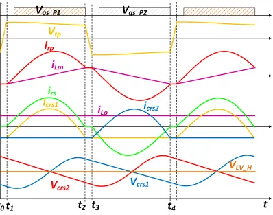
Figure 2-15 shows the detailed operation waveforms for the proposed CFSRC. It can be
found that the operating principle is similar to VFSRC. The only difference is the operation of resonant capacitor. In VFSRC, resonant capacitor participates in resonant during all times of switching cycle. While in CFSRC, resonant capacitor such as Crs1 will only join resonant
during half of switching cycle. It is clamped by output current during the other half switching cycle.
V
gs_P1V
gs_P2V
tpV
crs2i
rsi
Loi
crs1i
crs2t
0t
1t
2t
3t
V
crs1i
Lmi
rpV
LV_Ht
42.3.2 Time Domain Analysis
There are two operation modes within half switching cycle.
Mode 1 [t0 ~ t1]: This mode begins when P2 turns off at time t0. The resonant current irp is
negative and starts to charge the output capacitance Coss2 of P2 and discharge the output
P2 P1 Crp2 S1 S2 irp Co Crp1 n:1 Crs2 Crs1 Lm Lo iLm D1 D2 Coss1 Coss2 Ro irs Lrs
v
tp iLoCrp1 Crs1_eq
Lr iLin Lin iLin Lrp irp
icrp1 iCrs1_eq
icrs1
icrs2
icrp1
icrp2
V
MV_H(a) t1 ~ t2
P
2P1
C
rp2S
1S
2 irpC
o Crp1n:1
C
rs2 Crs1 Lm Loi
Lm D1D
2Cds1
Cds2R
oi
rsL
rsv
tpi
LoCrp2 Crs2_eq
i
Lo_eqLr iLin
L
in iLin Lrp irpi
crp2i
Crs2_eqi
crs1i
crs2i
crp1icrp2
V
MV_H(b) t3 ~ t4
capacitance Coss1 of P1. This mode is a transient mode important for achieving the ZVS
operation for P1.
Mode 2 [t1 ~ t2]: At time t1, the voltage on Coss1 is discharged to 0 and resonant current irp
flows through P1’s body diode. P1 turns on after t1 with ZVS, and irp resonates to its positive
half cycle. The equivalent circuit for time interval [t1 ~ t2] is shown in Figure 2-16. The input
and output inductors are treated as two current sources, iLin and iLo. The current difference
between iLin and irp flows into Crp1, while the difference between irp and iLo goes into Crs1. The
other resonant capacitors, Crp2 and Crs2, are clamped by iLin and iLo, respectively.
In Mode 2, the resonant tank contains four components: Lrp, Lrs, Crp1 and Crs1. The
equivalent resonant frequency of the resonant tank is derived as:
𝜔𝑟 = 1
√𝐿𝑟𝐶𝑟
2.5
where 𝐶𝑟 = 𝐶𝑟𝑝1𝐶𝑟𝑠1_𝑒𝑞
𝐶𝑟𝑝1+𝐶𝑟𝑠1_𝑒𝑞 , 𝐿𝑟 = 𝐿𝑟𝑝+ 𝐿𝑟𝑠_𝑒𝑞
𝐶𝑟𝑠1_𝑒𝑞 =𝐶𝑛𝑟𝑠12 , and 𝐿𝑟𝑠_𝑒𝑞 = 𝑛2𝐿𝑟𝑠.
Transient interval Mode 1, and the magnetizing current in Lm are neglected in the following
analysis for simplification. The equivalent differential equation during Mode 2 is derived in (2.6).
∫ 𝑖0𝑡 𝑐𝑟𝑝 1(𝜏)𝑑𝜏
𝐶𝑟𝑝1 = 𝐿𝑟
𝑑𝑖𝑟𝑝(𝑡)
𝑑𝑡 +
∫ 𝑖0𝑡 𝑐𝑟𝑠1_𝑒𝑞(𝜏)𝑑𝜏
𝐶𝑟𝑠1_𝑒𝑞 2.6
.
𝑑2𝑖 𝑟𝑝(𝑡)
𝑑𝑡2 + 𝜔𝑟2𝑖𝑟𝑝(𝑡) = 𝜔𝑟2𝑖𝐿𝑖𝑛 2.7
The solution for the resonant current can be derived
𝑖𝑟𝑝(𝑡) = 𝐼𝑟𝑠𝑖𝑛(𝜔𝑟𝑡 + 𝜑) + 𝑖𝐿𝑖𝑛 2.8
The resulting resonant current for Mode 2 is drawn in green curve in Figure 2-17, which
contains a resonant tank frequency component and a DC bias current of 𝑖𝐿𝑖𝑛. Note that the
resonant tank time interval Tr/2 is not equal to the current zero crossing time interval Tsw/2 in
Figure 2-17. This is very different with conventional VFSRC. This is due to the DC bias
current, iLin, introduced into the resonant current. Unity gain can only be achieved if the
0 T
sw/2 Tsw
T
r/2
φ
i
rpi
Lini
crp1t
φ
-i
LinT
sw/2
Figure 2-17 Equivalent current waveforms.
switching frequency, fs, is selected right at the current zero crossing. This frequency is the real
equivalent resonant frequency, 𝑓𝑧𝑐, for the CFSRC.
The operation principle of the other half switching cycle t2~t4 is symmetric to t0~t2 and the
resonant current for a full switching cycle is derived in equation (2.9). The result resonant current during entire switching cycle is drawn as red curve in Figure 2-17. In which the switching frequency is selected right at the current zero crossing. The result current has
sinusoidal shape.
𝑖𝑟𝑝(𝑡) = {𝐼𝐼𝑟sin(𝜔𝑟𝑡 − 𝜑) + 𝑖𝐿𝑖𝑛, 0 ≤ 𝑡 ≤ 𝑇𝑠/2
𝑟sin(𝜔𝑟𝑡 − 3𝜑) − 𝑖𝐿𝑖𝑛, 𝑇𝑠/2 ≤ 𝑡 ≤ 𝑇𝑠 2.9
To find the value of unknown parameters in equation (2.9), zero-crossing constraint of the resonant current is used
𝑖𝑟𝑝(0) = 𝐼𝑟sin(𝜑) + 𝑖𝐿𝑖𝑛= 0 2.10
The equation for current that flows through primary side capacitor Crp1 is derived in
equation (2.10).
𝑖𝑐𝑟𝑝1(𝑡) = {−𝐼𝑟𝑠𝑖𝑛(𝜔𝑟𝑡 + 𝜑),0 ≤ 𝑡 ≤ 𝑇𝑠/2
𝑖𝐿𝑖𝑛, 𝑇𝑠/2 ≤ 𝑡 ≤ 𝑇𝑠 2.11
The charging and discharging balance of the primary side capacitor, Crp1, is also applied.
Equation (2.12) is derived from (2.10) and (2.11).
tan (𝜑)(2𝜑
𝜋 + 1) =
2
Solving (2.12) provides a phase shift, 𝜑 = 0.458. The relationship between 𝜔𝑧𝑐 and 𝜔𝑟 is
then derived in (2.13).
𝑓𝑧𝑐 = 𝑓𝑟𝜋
𝜋 + 2𝜑 = 0.774𝑓𝑟 2.13
The result shows that the CFSRC’s zero crossing frequency, 𝜔𝑧𝑐, is 0.774 times of the resonant tank frequency, 𝜔𝑟. Switching frequency, fs, should be selected equal to fzc to achieve
unity gain.
2.3.3 Fundamental Harmonic Approximation
In addition to the time domain analysis, analysis based on FHA method is also conducted
for verification.
The secondary side current can be represented with a switching frequency sinusoidal
current ir_F(t). The current flow through secondary side resonant capacitor Crs1 can be describe
in equation
𝐼𝑐𝑟1(𝑡) = {𝑖𝑟_𝐹−𝐼(𝑡) − 𝐼𝑜, 0 ≤ 𝑡 ≤ 𝑇𝑠/2
𝑜, 𝑇𝑠/2 ≤ 𝑡 ≤ 𝑇𝑠 2.14
Equation (2.15) can be derived based on Crs1’scharging and discharging balance.
𝑖𝑟_𝐹(𝑡) = 𝜋𝐼𝑜𝑠𝑖𝑛(𝜔𝑠𝑡) 2.15
The secondary side half bridge mid terminal voltage Vac in Figure 2-18 is provided in
equation (2.16). The waveform of Vac is drawn in Figure 2-21.
S
1S
2C
oC
rs2C
rs1L
oR
oi
rsI
oV
ac+
-
V
o+
-V
CT+
Figure 2-18 Secondary side circuit
0
0 Tsw/2 Tsw
t
i
r
i
r_F
Figure 2-19 Current approximation.
𝑉𝑎𝑐(𝑡) = { 𝑉𝑐𝑟𝑠1(𝑡), 0 ≤ 𝑡 ≤ 𝑇𝑠/2
−𝑉𝑐𝑟𝑠2(𝑡), 𝑇𝑠/2 ≤ 𝑡 ≤ 𝑇𝑠 2.16
Currents that flow through secondary capacitors Crs1 and Crs2 are list in equation (2.17) and
(2.18)
𝐼𝑐𝑟1(𝑡) = {𝜋𝐼𝑜sin(𝜔𝑠𝑡) − 𝐼𝑜, 0 ≤ 𝑡 ≤ 𝑇𝑠/2
−𝐼𝑜, 𝑇𝑠/2 ≤ 𝑡 ≤ 𝑇𝑠 2.17
𝐼𝑐𝑟2(𝑡) = {−𝜋𝐼 −𝐼𝑜, 0 ≤ 𝑡 ≤ 𝑇𝑠/2
𝑜sin(𝜔𝑠𝑡) − 𝐼𝑜, 𝑇𝑠/2 ≤ 𝑡 ≤ 𝑇𝑠
2.18
Figure 2-20 Secondary side resonant capacitor voltage
During half of the switching cycle, the secondary capacitor Crs1 are discharging with the
output current. Therefore, the capacitor ripple voltage on these secondary resonant capacitors
is derived as
∆𝑉𝑐𝑟𝑠 = 𝑇𝑠𝐼𝑜
2𝐶𝑟𝑠 =
𝜋𝐼𝑜
𝜔𝑠𝐶𝑟𝑠 2.19
The voltage waveforms of secondary resonant capacitors Crs1 and Crs2 are shown in Figure
2-20. The total voltage VCT shown in same figure is the combination of voltages on Crs1 and
Crs2. This figure shows that although voltage on resonant capacitor has large ripple voltage,
these ripple voltages will cancel each other and form a low ripple voltage output voltage. This
figure also shows that Crs1 and Crs2 not only act as resonant capacitors, but also work as filter
capacitors to the output side.
Voltages equations on these capacitors can be derived as
𝑉𝑐𝑟1(𝑡) =
{ 𝑉𝑜 2 − ∆𝑉𝑐𝑟𝑠 2 + 𝜋𝐼𝑜
𝜔𝑠 (1 − cos(𝜔𝑠𝑡)) − 𝐼𝑜𝑡
𝐶𝑟𝑠 , 0 ≤ 𝑡 ≤ 𝑇𝑠/2
𝑉𝑜
2 +
∆𝑉𝑐𝑟𝑠
2 −
𝐼𝑜(𝑡 −𝑇2 )𝑠
𝐶𝑟𝑠 , 𝑇𝑠/2 ≤ 𝑡 ≤ 𝑇𝑠
2.20
𝑉𝑐𝑟2(𝑡) =
{ 𝑉𝑜 2 + ∆𝑉𝑐𝑟𝑠 2 − 𝐼𝑜𝑡
𝐶𝑟𝑠, 0 ≤ 𝑡 ≤ 𝑇𝑠/2
𝑉𝑜
2 −
∆𝑉𝑐𝑟𝑠
2 +
𝜋𝐼𝑜
𝜔𝑠 (1 + cos(𝜔𝑠𝑡)) − 𝐼𝑜(𝑡 −𝑇2 )𝑠
𝐶𝑟𝑠 , 𝑇𝑠/2 ≤ 𝑡 ≤ 𝑇𝑠
2.21
𝑉𝑎𝑐(𝑡) =
{
𝑉𝑜
2 −
𝜋𝐼𝑜(cos(𝜔𝑠𝑡))
𝜔𝑠𝐶𝑟𝑠 +
∆𝑉𝑐𝑟𝑠
2 −
𝐼𝑜𝑡
𝐶𝑟𝑠, 0 ≤ 𝑡 ≤ 𝑇𝑠/2
−𝑉𝑜
2 −
𝜋𝐼𝑜(cos(𝜔𝑠𝑡))
𝜔𝑠𝐶𝑟𝑠 −
∆𝑉𝑐𝑟𝑠
2 +
𝐼𝑜(𝑡 −𝑇2 )𝑠
2 , 𝑇𝑠/2 ≤ 𝑡 ≤ 𝑇𝑠
2.22
where ∆𝑉𝑐𝑟𝑠 = 𝜋𝐼𝑜
𝜔𝑠𝐶𝑟𝑠 is the ripple voltage of capacitors Crs1 and Crs2.
Investigating equation (2.22), voltage Vac can be divided into three parts: (i) a square
waveform, 𝑉𝑠𝑞(𝑡), (ii) a cosine waveform, 𝑉𝑐𝑜𝑠(𝑡), and (iii) a triangular waveform, 𝑉𝑡𝑟𝑖(𝑡). Vac
and the three associated components, expressed mathematically in (2.23) – (2.25), are drawn
in Figure 2-21.
Vac
V
cosV
sqV
tri0 T
sw/2 Tsw t
𝑉𝑠𝑞(𝑡) = { 𝑉𝑜
2, 0 ≤ 𝑡 ≤ 𝑇𝑠/2
−𝑉𝑜
2 , 𝑇𝑠/2 ≤ 𝑡 ≤ 𝑇𝑠
2.23
𝑉𝑐𝑜𝑠(𝑡) =−𝜋𝐼𝑜(cos(𝜔𝜔 𝑠𝑡))
𝑠𝐶𝑟𝑠 2.24
𝑉𝑡𝑟𝑖(𝑡) =
{
∆𝑉𝑐𝑟𝑠
2 +
−𝐼𝑜𝑡
𝐶𝑟𝑠 , 0 ≤ 𝑡 ≤ 𝑇𝑠/2
−∆𝑉𝑐𝑟𝑠
2 +
𝐼𝑜(𝑡 −𝑇𝑠 2 )
𝐶𝑟𝑠 , 𝑇𝑠/2 ≤ 𝑡 ≤ 𝑇𝑠
2.25
FHA method is used to find the fundamental harmonic of the three derived elements. Fundamental components of each component are provided in (2.26) – (2.28). The associated
fundamental curves are drawn Figure 2-22.
𝑉𝑠𝑞_𝐹(𝑡) =
2𝑉𝑜
𝜋 𝑠𝑖𝑛(𝜔𝑠𝑡) 2.26
𝑉𝑐𝑜𝑠(𝑡) =
−𝜋𝐼𝑜(cos(𝜔𝑠𝑡))
𝜔𝑠𝐶𝑟𝑠 2.27
𝑉𝑡𝑟𝑖_𝐹(𝑡) = 4𝐼𝑜
𝜋𝜔𝑠𝐶𝑟𝑠𝑐𝑜𝑠(𝜔𝑠𝑡) 2.28
The resulting half bridge voltage can be simplified as
The impedance seeing from the half bridge can be found through dividing 𝑉𝑎𝑐_𝐹 by 𝑖𝑟_𝐹(𝑡).
Three equivalent components can be found as shown in Figure 2-23, a resistor, a capacitor,
and an inductor.
The value of each component is found in (2.30) – (2.32).
𝑅𝑎𝑐 =
𝑉𝑠𝑞_𝐹(𝑡)
𝑖𝑟_𝐹(𝑡) =
2
𝜋2𝑅𝑜 2.30
𝐶𝑒𝑞𝑠= 𝑑𝑉𝑖𝑟_𝐹(𝑡)
𝑐𝑎𝑝(𝑡) 𝑑𝑡
= 𝐶𝑟𝑠 2.31
𝐿𝑒𝑞𝑠= 𝑉𝑡𝑟𝑎𝑛_𝐹𝑑𝑖 (𝑡) 𝑟𝐹(𝑡)
𝑑𝑡
= 4
𝜋2𝜔
𝑠2𝐶𝑟𝑠 2.32
0 Tsw/2 Tsw t
V
triVcos
V
sqV
tri_FV
sq_FFigure 2-22 Fundamental components approximation.
After completing the same analysis on the primary side, the AC equivalent circuit for the proposed CFSRC is shown in Figure 2-24. Different from VFSRC circuit, where the resonant
capacitors are 2𝐶𝑟𝑝 and 2𝐶𝑟𝑠_𝑒𝑞, the result resonant capacitors in proposed CFSRC are 𝐶𝑟𝑝 and
L
eqs
L
r_eq
i
r_F
C
eq
R
ac
V
ac
+
-V
o
+
Figure 2-23 Equivalent frequency domain circuit.
L
eqs
L
r_eq
i
r
C
eqs
R
ac
L
eqp
C
eqp
Z≈
0
V
d_F
.
in resonant. However, CFSRC introduced two additional inductor components, 𝐿𝑒𝑞𝑝 𝑎𝑛𝑑 𝐿𝑒𝑞𝑠,
into the circuit. These two inductors are associated with the capacitor on each side. The equivalent total resonant inductance of the whole system is
𝐿𝑒𝑞 = 𝐿𝑒𝑞𝑠+ 𝐿𝑒𝑞𝑝+ 𝐿𝑟 = 4
𝜋2𝜔
𝑠2 1
𝐶𝑟_𝑒𝑞+ 𝐿𝑟 2.33
Where
𝐿𝑒𝑞𝑠 = 𝜋2𝜔4
𝑠2𝐶𝑒𝑞𝑠, 𝐿𝑒𝑞𝑝=
4 𝜋2𝜔𝑠2𝐶𝑒𝑞𝑝.
𝑅𝑎𝑐 = 𝑛2 2
𝜋2𝑅𝑜, 𝐶𝑒𝑞𝑝 = 𝐶𝑟𝑝, 𝐶𝑒𝑞𝑠 =
1 𝑛2𝐶𝑟𝑠 The system equivalent resonant frequency is then obtained as
𝜔𝑧𝑐2 =
1
𝐶𝑟𝐿𝑒𝑞 =
1 𝐶𝑟(𝜋24𝜔
𝑠2 1
𝐶𝑟+ 𝐿𝑟) 2.34
Notice that (2.32) contains a switching frequency, 𝜔𝑠, and a system equivalent resonant
frequency, 𝜔𝑧𝑐. If the switching frequency is selected to be the same as the equivalent resonant
frequency, 𝜔𝑧𝑐 = 𝜔𝑠. Equation (2.35) can be derived.
𝑓𝑧𝑐 = √1 − 4𝜋2
√𝐶𝑟𝐿𝑟
= 0.771
√𝐶𝑟𝐿𝑟
= 0.771𝑓𝑟 2.35
This result is consistent with the result obtained in time domain analysis, which indicates
that the proposed CFSRC circuit equivalent system resonant frequency is 0.771 times of the resonant tank frequency. The switching frequency should be selected at frequency, fzc, to
2.3.4 Voltage Gain Investigation
Base on the FHA method, a relevant AC equivalent circuit of the proposed CFSRC is derived in Figure 2-24. In order to derive the voltage gain equation for the proposed circuit, a more accurate AC equivalent circuit that contains magnetizing inductance Lm is provided in
Figure 2-25 for voltage gain investigation.
Parameters in Figure 2-25 are 𝑅𝑎𝑐 = 𝑛2 2𝜋2𝑅𝑜, 𝐶𝑒𝑞𝑝 = 𝐶𝑟𝑝, 𝐶𝑒𝑞𝑠 =
1 𝑛2𝐶𝑟𝑠
𝐿𝑒𝑞𝑠 =𝜋2𝜔4
𝑠2𝐶𝑒𝑞𝑠, 𝐿𝑒𝑞𝑝=
4 𝜋2𝜔𝑠2𝐶𝑒𝑞𝑝
Lrp and Lrs are equivalent leakage inductance distributed on two sides of the transformer.
Total equivalent voltage gain can be calculated as
𝑀
𝜔𝐿 𝑅 2.36
L
eqsL
rpC
eqsR
acL
eqpC
eqpL
rsL
mV
d_FWhere 𝐿𝑙𝑘𝑝 = 𝐿𝑒𝑞𝑝+ 𝐿𝑟𝑝, 𝐿𝑙𝑘𝑠 = 𝐿𝑒𝑞𝑠+ 𝐿𝑟𝑠. S1 S2 irp Co n:1 Crs2 Crs1 Lm Lo Ro Lr P2 P1 Crp2 Crp1 Cin
Vin Vo
Leqs
Lr
ir
Ceqs
Ceqp
≈
0
(a) Type 2
S1 S2 irp Co n:1 Crs2 Crs1 Lm Lo Ro Lr P2 P1 Cin Vin P3
P4 Crp
Vo Leqs Lr ir Ceqs Ceqp
≈
0
(b) Type 3
P2 P1 Crp2 irp Crp1 n:1 Lm Lin iLin Lr S2 Co Crs1 Ro Crs2 Vo S1 Leqs Lr ir Ceqs Ceqp
≈
0
(c) Type 4
P2 P1 Crp2 irp Crp1 n:1 Lm Lin iLin Lr S2
Co Ro Vo
S1 S3
S4 Crs Leqs Lr ir Ceqs Ceqp
≈
0
(d) Type 5
2.3.5 Extension Application of ICF Cell
The introducing of HF ICF cell into SRC doesn’t affect the resonant tank current shape. However, it will affect the equivalent zero current crossing frequency.
In practical applications, the HF ICF cell can be used together with conventional voltage fed bridge cell.
A family of SRC circuits based on HF ICF cell and voltage based bridge are provide in
Figure 2-26 (a)- (d). All circuits here reserves AC shape current in resonant tank. Which not only helps realize ZVS operation of primary side switches over wide load range, but also helps
obtain low turn off current to minimize switching loss. The ac equivalent circuits based on FHA method are provided as well. These derived circuit can be useful in practical applications.
Table 2-2 Current Zero Crossing Equivalent Frequency
Symbol Crp_eq Crs_eq Ceq Leq fzc Gain
CFSRC Crp Crs
𝐶𝑟𝑝𝐶𝑟𝑠 𝐶𝑟𝑝+ 𝐶𝑟𝑠
4 𝜋2𝜔
𝑠2 1 𝐶𝑒𝑞+ 𝐿𝑟
√1 − 4𝜋2 √𝐶𝑒𝑞𝐿𝑟
1
Type 2 2Crp Crs
2𝐶𝑟𝑝𝐶𝑟𝑠 2𝐶𝑟𝑝+ 𝐶𝑟𝑠
![Figure 2-2 Dual Active Bridge based AC-AC converter circuit used in [30]](https://thumb-us.123doks.com/thumbv2/123dok_us/1173789.1147546/30.612.107.521.310.513/figure-dual-active-bridge-based-converter-circuit-used.webp)
![Figure 2-3 SST with direct AC-AC isolated front end based on SRC circuit [11]](https://thumb-us.123doks.com/thumbv2/123dok_us/1173789.1147546/31.612.131.501.350.588/figure-sst-direct-ac-isolated-based-src-circuit.webp)