Optimal ZVS modulation of single-phase single-stage
bidirectional DAB AC-DC converters
Citation for published version (APA):
Everts, J., Krismer, F., Van den Keybus, J., Driesen, J., & Kolar, J. W. (2014). Optimal ZVS modulation of single-phase single-stage bidirectional DAB AC-DC converters. IEEE Transactions on Power Electronics, 29(8), 3954-3970. https://doi.org/10.1109/TPEL.2013.2292026
DOI:
10.1109/TPEL.2013.2292026
Document status and date: Published: 01/01/2014
Document Version:
Publisher’s PDF, also known as Version of Record (includes final page, issue and volume numbers)
Please check the document version of this publication:
• A submitted manuscript is the version of the article upon submission and before peer-review. There can be important differences between the submitted version and the official published version of record. People interested in the research are advised to contact the author for the final version of the publication, or visit the DOI to the publisher's website.
• The final author version and the galley proof are versions of the publication after peer review.
• The final published version features the final layout of the paper including the volume, issue and page numbers.
Link to publication
General rights
Copyright and moral rights for the publications made accessible in the public portal are retained by the authors and/or other copyright owners and it is a condition of accessing publications that users recognise and abide by the legal requirements associated with these rights. • Users may download and print one copy of any publication from the public portal for the purpose of private study or research. • You may not further distribute the material or use it for any profit-making activity or commercial gain
• You may freely distribute the URL identifying the publication in the public portal.
If the publication is distributed under the terms of Article 25fa of the Dutch Copyright Act, indicated by the “Taverne” license above, please follow below link for the End User Agreement:
www.tue.nl/taverne
Take down policy
If you believe that this document breaches copyright please contact us at:
providing details and we will investigate your claim.
Optimal ZVS Modulation of Single-Phase
Single-Stage Bidirectional DAB AC–DC Converters
Jordi Everts, Member, IEEE, Florian Krismer, Member, IEEE, Jeroen Van den Keybus,
Johan Driesen, Senior Member, IEEE, and Johann W. Kolar, Fellow, IEEE
Abstract—A comprehensive procedure for the derivation of
op-timal, full-operating-range zero voltage switching (ZVS) modu-lation schemes for single-phase, single-stage, bidirectional and isolated dual active bridge (DAB) ac–dc converters is presented. The converter topology consists of a DAB dc–dc converter, re-ceiving a rectified ac line voltage via a synchronous rectifier. The DAB comprises primary and secondary side full bridges, linked by a high-frequency isolation transformer and a series induc-tor. ZVS modulation schemes previously proposed in the liter-ature are either based on current-based or energy-based ZVS analyses. The procedure outlined in this paper for the calcula-tion of optimal DAB modulacalcula-tion schemes (i.e., combined phase-shift, duty-cycle, and switching frequency modulation) relies on a novel, more accurate, current-dependent charge-based ZVS analysis, taking into account the amount of charge that is re-quired to charge the nonlinear parasitic output capacitances of the switches during commutation. Thereby, the concept of “com-mutation inductance(s)” is shown to be an essential element in achieving full-operating-range ZVS. The proposed methods are applied to a 3.7 kW, bidirectional, and unity power fac-tor electric vehicle battery charger which interfaces a 400 V dc-bus with the 230Va c, 50-Hz utility grid. Experimental results
obtained from a high-power-density, high-efficiency converter pro-totype are given to validate the theoretical analysis and practical feasibility of the proposed strategy.
Index Terms—AC–DC power conversion, battery charger,
cir-cuit analysis, dual active bridge (DAB), optimal control.
I. INTRODUCTION
S
INGLE-PHASE, utility interfaced, isolated ac–dc convert-ers with power factor correction (PFC) cover a wide range of applications such as chargers for plug-in hybrid electrical vehicles and battery electric vehicles [1], [2], interfaces for residential dc distribution systems and energy storage systems [3], [4], and inverters for photovoltaic modules. Bidirectional power flow is increasingly required since the traditional electric-ity grid is evolving from a rather passive to a smart interactiveManuscript received June 29, 2013; revised October 6, 2013; accepted November 7, 2013. Date of current version March 26, 2014. Recommended for publication by Associate Editor P. Barbosa.
J. Everts and J. Driesen are with the Department of Electrical Engineer-ing, division ELECTA, KU Leuven, Heverlee-Leuven 3001, Belgium (e-mail: [email protected]; [email protected]).
F. Krismer and J. W. Kolar are with the Power Electronic Systems Labora-tory, ETH Z¨urich, Z¨urich 8092, Switzerland (e-mail: [email protected]; [email protected]).
J. Van den Keybus is with the Triphase N.V., Heverlee-Leuven 3001, Belgium (e-mail: [email protected]).
Color versions of one or more of the figures in this paper are available online at http://ieeexplore.ieee.org.
Digital Object Identifier 10.1109/TPEL.2013.2292026
service network (customers/operators), where energy systems play an active role in providing different types of support to the grid [5] (e.g., vehicle-to-grid (V2G) concepts [6] and dc distribution systems [3]).
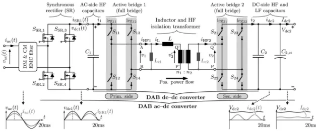
It is shown in [7] and [8] that the above mentioned unity power factor, isolated ac–dc conversions can be realized by combining a line voltage rectifier with a dual active bridge (DAB) dc–dc converter (single power conversion stage). For the line voltage rectifier, besides a passive diode bridge, an efficient synchronous rectifier (SR) can be used to further reduce the conduction losses and to enable bidirectional power flow. As no energy storage is present in the dc-link (a small high-frequency (HF) filter capacitor is placed between the SR and the DAB), the PFC is performed by the DAB, which has to actively shape the line current. The biggest advantage of these DAB topologies is that the ac–dc energy conversions take place in a single conversion stage (1-S), producing high quality waveforms and complying to regulations on low- and high-frequency distortions of the mains ac power lines [8]–[10]. Compared to the traditional dual-stage (2-S) approaches [4], a power factor correcting front-end as well as bulky failure prone electrolytic dc-link capacitors are omitted [11]. The 1-S DAB ac–dc converter topology implemented with a full bridge–full bridge (FBFB) DAB and SR (bidirectional power flow), as shown in Fig. 1, is the subject of this paper.
Research on the DAB mainly has been focusing on improved modulation schemes which facilitate increased converter effi-ciency and/or power density [12]. Whether the DAB is used in a dc–dc, a 1-S ac–dc (this paper), or any other configuration, one of the main goals has been to optimally (i.e., minimizing a certain, mostly loss related, cost function) operate the DAB within conditions where quasi-zero switching losses occur (i.e, by virtue of zero voltage switching, ZVS). Therefore, publica-tions on DAB modulation schemes can be classified according to their ZVS considerations.
1) Current-based (CB) ZVS: The largest group of publications does not take into account the (parasitic) switch capacitances and assumes that ZVS of a bridge leg is achieved when the drain-to-source current of the switch which initiates the commutation (turn-off) is positive at the switching instant. Besides the tradi-tional phase-shift-modulation (PSM1), where full-power-range
CB ZVS is only possible at a voltage conversion ratio2dequal
to one [8], [13], modulation schemes with increased degree of freedom regarding the search toward optimal CB ZVS operation
1PSM: the active bridges of the DAB are operated to generate 50% duty-cycle
high-frequency ac-link voltages which are phase-shifted relative to each other in order to achieve the required power transfer (one degree of freedom).
2According to Fig. 1,d=n
1/n2·Vd c 2/vd c 1.
0885-8993 © 2013 IEEE. Personal use is permitted, but republication/redistribution requires IEEE permission. See http://www.ieee.org/publications standards/publications/rights/index.html for more information.
Fig. 1. Circuit schematic of the single-phase, single-stage (1-S), bidirectional and isolated DAB ac–dc converter topology. of the DAB are introduced. These schemes combine PSM with
either single-sided duty-cycle modulation (further referred to as SSPWM) or dual-sided duty-cycle modulation (further referred to as DSPWM; highest degree of freedom), and use a low-power and a high-power switching mode3 in order to reduce the HF
ac-link rms currents, to lower the transformer core flux, and to obtain full-operating-range CB ZVS [14]. Especially, DSPWM enables significant improvements for low-load operation and for widely varying input and/or output voltage ranges such as is the case for the investigated 1-S ac–dc converter, where the DAB input voltage is a rectified sinewave (see Fig. 1), and where
dis highly variable [11]. Simple suboptimal solutions for the calculation of the modulation parameters in order to achieve full-operating-range CB ZVS are given in [15] and [16] using SSPWM, and in [9] using DSPWM. An SSPWM scheme for minimizing the reactive inductor power is presented in [17]. In [12], an optimal DSPWM scheme with respect to minimum inductor rms currents is proposed.
2) Energy-based (EB) ZVS: It was already shown in [18] that when considering CB ZVS, substantial parts of the ZVS regions involve incomplete bridge commutations due to the presence of (parasitic) switch capacitances. Consequently, above modula-tion schemes result in (partly) hard-switching operamodula-tion for cer-tain intervals of the DAB’s operating range,4leading to reduced
efficiency and in the worst case destruction of the semiconduc-tor switching devices. The influence of the switch capacitances on the (resonant) bridge commutations is described in [10] and [18]–[21] by evaluating the energy balance between the switch capacitances and the HF ac-link inductances (EB ZVS). However, in [10] and [19], the state of the one active bridge is not taken into account in the ZVS verification of the other, lead-ing to easy implementable but incomplete EB ZVS constraints. A simple suboptimal modulation scheme based on these simpli-fied constraints is presented in [10] using SSPWM and variable
3The low-power and high-power modes are similar to, respectively, mode 2
and mode 1 in this paper (cf. Fig. 7).
4This effect is most pronounced in the regions whered1andd1, and
along the boundary between the low- and the high-power mode [18].
switching frequency (fs) control.5 However, EB ZVS could
not be fully achieved for the low-power mode, and the tran-sition between the low- and high-power modes encompasses highly undesirable discontinuous steps in the modulation pa-rameters. The harder to implement EB ZVS constraints given in [18], [20], and [21], are still incomplete as the state of the one active bridge is taken into account in the ZVS verification of the other but, however, a (quasi) simultaneous state change within the one and/or together with the other active bridge is not allowed. Therefore, in [20], simplifications had to be made, yielding a suboptimal modulation scheme which uses DSPWM and variablefs. Full-operating-range EB ZVS was reported but,
again, the mode transition involves discontinuous steps. Regardless their objective, all DAB modulation schemes so far presented are based on “theoretical” CB or EB ZVS analyses. The latter are the most accurate but, as described previously, still involve difficulties, in particular concerning implementability and accuracy. As a consequence, the objective of this paper is twofold. On the one hand, this paper attempts to deal with the deficiencies of the CB and EB ZVS considerations by proposing a current-dependent charge-based (CDCB) ZVS analysis (see Section III) that takes into account the commuta-tion charge of the (parasitic) switch capacitances6as well as the
time dependence of the commutation currents. Therewith, the state and the simultaneous and nonsimultaneous state changes of the active bridges are inherently dealt with, resulting in a more accurate description of the DAB’s ZVS conditions. On the other hand, a procedure to derive optimal ZVS modulation schemes (see Section IV) for DAB converters is introduced and illustrated for the investigated 1-S DAB ac–dc converter. This procedure combines DSPWM and frequency modulation in order to minimize a cost function related to the converter losses, and relies on the proposed CDCB ZVS analysis in order to assure full-operating-range ZVS. Furthermore, the concept
5In [22], it was shown that the use of a variable switching frequencyf
s
enables improved DAB efficiency.
6The EB ZVS analyses are typically based on constant energy-equivalent
switch capacitances [10]. As this can result in significant errors [23], in this paper the voltage dependent nonlinear switch capacitances are correctly modeled using data-sheet small-signal measurements (see Section III).
TABLE I
CONVERTERSPECIFICATIONS ANDREQUIREMENTS
of “commutation inductance(s),”7which is implemented in the calculation procedure, is introduced as an essential element in achieving both full-operating-range ZVS and smooth, contin-uous mode transitions. As explained previously and reaffirmed in Section IV, these two objectives are normally problematic for DAB converters with large input and/or output voltage variations and large power variations such as is the case for the single-stage DAB ac–dc converter investigated in this paper.
The paper is further organized as follows. In Section II, af-ter a brief discussion of the general operating principle of the single-stage DAB ac–dc converter, a simplified representation of the DAB converter is given and the operating modes are de-tailed. The implications on the model and the expressions by adding commutation inductance(s) in the HF ac-link are de-scribed. In Section III, the CDCB ZVS analysis is introduced, followed by the procedure to determine optimal ZVS modu-lation schemes and optimal system level component values in Section IV. In Section IV-B, the results obtained from numeri-cal optimizations are given for different HF ac-link configura-tions, highlighting the necessity of commutation inductance(s) in achieving full-operating-range ZVS. The actual implemen-tation of the calculated modulation schemes (see Section V-A) and the experimental results (see Ssection V-B) obtained from a 3.7 kW, bidirectional, and unity power factor 1-S DAB ac–dc prototype system are presented in Section V.
The specifications (see Table I) of the investigated DAB ac–dc converter shown in Fig. 1 are based on the requirements for future electric vehicle on-board battery chargers, interfacing a400V dc-bus with the single-phase 230 Vrm s/50 Hz mains.
Compliance with domestic power sockets results in a nomi-nal (active) ac input current ofIac,P= 16Arm sand a nominal
power ofPnom = 3.7kW. The voltage ranges are further listed
in Table I. The dc-bus voltage level was chosen based on the forecasts that the vehicular power system voltages tend to rise. Bidirectional power flow enables V2G functionality, while gal-vanic isolation ensures safety. Other requirements are a high conversion efficiency, a high power density, EMC compliance to the CISPR 22 Class B standard, a high power factor (PF), and low total harmonic distortion (THD) of the ac input current (see Table I).
7It has been mentioned in inter alia [9], [16], [18] that the magnetizing
inductance of the transformer can be used to provide additional commutation charge in the switches. However, no detailed investigation (and subsequent modulation scheme) concerning EB (or CDCB) ZVS is given.
Fig. 2. Equivalent circuit of the converter’s ac input side, with a controllable current sourceiD A B 1, the SR, and the two-stage DM EMC filter.
II. ANALYSIS OF THEDAB MODEL A. DAB ac–dc Converter Topology
Fig. 1 shows the schematic of the single-phase, single-stage, bidirectional and isolated DAB ac–dc converter topology, con-sisting of an SR followed by a DAB dc–dc converter. During operation, the state stSR of the SR changes two times each
period of the ac line voltagevac(t), according to
stSR =
1 ifvac(t)>0 (SSR,1& SSR,4 are on) −1 ifvac(t)<0 (SSR,2& SSR,3 are on). (1)
Due to this continuous state change, the ac line voltagevac(t)
is folded into a dc voltagevdc1(t) that is pulsating twice the
ac line frequencyfL(i.e.,vdc1(t) =|vac(t)|=|Vˆacsin(ωLt)|)
and that is directly fed to the input of the DAB dc–dc converter. Note that the voltage drop across the differential mode (DM) input filter inductors can be neglected in a steady state. As explained in Section II-B, the DAB draws a net dc currenti1
at its input. The HF components ofi1 are bypassed by a small
HF filter capacitorC1 that is placed between the SR and the
DAB, while the dc componentiDA B1 (not shown in Fig. 1) of
i1 propagates to the SR. In the ideal case, i.e., neglecting the
reactive power consumed by the HF filter capacitorC1,8the SR’s
output currentiSR 1(t)equalsiDA B1(t). By proper modulation
of the DAB’s active bridges this current iDA B1(t), and thus
iSR 1(t), can be actively controlled to be in phase withvdc1(t).
AsiSR 1(t)is unfolded toward the ac input side by the SR, a
sinusoidal ac input currentiac(t)that is in phase (unity power
factor) with the ac input voltagevac(t)is obtained. However,
in the nonideal case, the reactive (capacitive) power consumed byC1and by the other DM EMC input filter capacitor(s) needs
to be compensated in order to meet the PFC requirement given in Table I. This can be done by controllingiDA B1(t)slightly
lagging tovdc1(t), requiring a certain reactive power transfer
capability of the DAB. For the exact calculation ofiDA B1(t), in
Fig. 2 the DAB is represented by a variable current sourceiDA B1
connected in parallel with the DM EMC input filter and the SR (note thatC1 is the capacitive part of the first DM filter stage,
CD M 1 =C1). It can be shown9 that for a given amplitude of
the (active) ac input currentIˆac∗,Pand PF (= cos(ϕ); see Fig. 3),
8Voltagev
d c 1(t)induces a small capacitive current inC1.
9In a steady statei
Fig. 3. Ideal input-side quantities for the worst case PF condition:Iˆa c∗ ,P =
√
2·0.1·Ia c,P,n o m= 2.26A;Vˆa c = ˆVa c,m a x = 357.8V; PF= 0.9.
iDA B1needs to be controlled according to
iDA B1 =stSR
dir·( ˆIac∗,P/PF) sin(ωLt+dir·arccos(PF)) −ωL(CD M 1+CD M 2) ˆVacsin(ωLt+π/2)
(2) where ωL= 2πfL withfL the 50 Hz ac line frequency, Vˆac
the amplitude of the ac input voltage,stSR the state of the SR
[according to (1)], anddirthe power flow direction (see Fig. 1)
dir=
1 ifp(t)>0 :prim.→sec. side,
−1 ifp(t)<0 :sec.→prim. side. (3)
The ideal converter’s input-side quantities for the worst case PF condition (Table I; Iˆac∗,P =√2·0.1·Iac,P,nom = 2.26A;
ˆ
Vac= ˆVac,m ax = 357.8 V; PF= 0.9) are depicted in Fig. 3.
The values of CD M 1 (=C1) and CD M 2 are listed in
Ta-ble IV. In order to meet the PFC requirements (see TaTa-ble I) under all input conditions, including enough current mar-gin for component variances, an upper DAB input current limit iDA B1,u is calculated. Assuming PF= 1, dir= 1, and
CD M 1=CD M 2= 0, the instantaneousiDA B1 according to (2)
becomesiDA B1=stSRIˆac∗,Psin(ωLt) =|Iˆac∗,Psin(ωLt)|. This
means that theiDA B1, which corresponds with a certain value
of the DAB input voltage vdc1=|vac|=|Vˆacsin(ωLt)| and
ac input currentIˆac∗,P, can be calculated withiDA B1 = ˆIac∗,P·
vdc1/Vˆac. Consequently iDA B1 at a certain vdc1 and for a
certainIˆac∗,P is highest ifVˆac= ˆVac,m in. UsingIˆac∗,P = 24A
(=√2·Iac,P,nom+ margin), adding a margin of 0.5 A, and
clamping the result to 24 A,iDA B1,uis defined as10
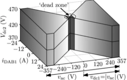
iDA B1,u(vdc1) = min 24·vdc1 ˆ Vac,m in + 0.5,24A . (4) Taking the lower limitiDA B1,l=−iDA B1,uyields the complete
converter’s operating range11shown in Fig. 4. Note that the DAB handles the double-line frequency power component, which in
10Given the specifications in Table I, the current margins were chosen to be
able to satisfy (2) at any possible input condition (Va c, Ia c,P, and PF) that may
occur, taking into account component variances. The selection of the margins thus depends on the final hardware design.
11Around the zero crossing (−30Vv
a c30V) the bridges of the DAB
are inactive (dead zone) as ZVS power conversion is quasi-impossible within this voltage interval (see also Section IV).
Fig. 4. Complete operating range of the investigated DAB converter.
Fig. 5. Simplified (lossless) electrical model of the DAB.
the 2-S ac-dc topologies is buffered by the (electrolytic) dc-link capacitor. Due to the absence of this dc-dc-link capacitor in the investigated single-stage converter, an electrolytic capacitor
C2,stwas placed at the dc output side in order to (partly) filter
the 100-Hz power component. B. Simplified DAB Model
The DAB in Fig. 1 comprises HF transformer-coupled pri-mary and secondary side full bridges, performing the PFC [via active control ofiDA B1 according to (2)] and the regulation of
dc output voltageVdc2. Therefore, they produce phase-shifted
edge resonant square wave voltagesv1andv2at the terminals of
the HF ac-link (inductorLand HF transformer), resulting in an inductor currentiL. Both active bridges act as ac–dc converters
to their respective dc side, transforming the ac currents iH F1
andiH F2into net dc currentsi1andi2. Filter capacitorsC1and
C2 bypass the HF components ofi1 andi2. The respective dc
components (iDA B1andiDA B2; not shown in Fig. 1) propagate
to the input and the output of the DAB, and are obtained by av-eragingi1(t), respectively.i2(t)over the one switching period
Ts = 1/f s, e.g. iDA B1 =i1,avg = 1 Ts t0+Ts t0 i1(t)dt. (5)
On the assumption of ideal components and by referring the model to the primary side of the transformer, a simpli-fied (lossless) electrical representation of the DAB is obtained (see Fig. 5). The primary side referred voltagev2 is given by
v2=v2·n1/n2. By applying an appropriate phase shift angle12
φ between the voltages v1 and v2 and additionally adjusting
the respective pulse width modulation angles τ1 andτ2 (i.e.,
DSPWM;τ1, τ2are defined in Fig. 6),iDA B1can be controlled.
A last parameter that can be freely adjusted (within a reasonable
12The phase shift angleφis defined as the angle between the first falling edge
Fig. 6. Influence ofLc 1 andLc 2on the HF ac-link currents for (a) mode1+
and (b) mode 2, using the same conditions as in Fig. 7 (see caption). (a) Mode
1+; with primary side commutation current (top inset); with secondary side commutation current (bottom inset). (b) Mode 2; with primary side commutation current (top inset); with secondary side commutation current (bottom inset).
range) is the switching frequencyfs, resulting in a total of four
modulation parameters:x= (φ, τ1, τ2, fs).
C. Switching Modes and Commutation Inductance(s)
As presented in [12, Fig. 2], depending on the sequence in time of the falling and rising edges of the voltagesv1 andv2,
twelve different switching modes13 can be generated with the
DAB shown in Fig. 1. It is shown in Section IV that only two out of the twelve possible modes are feasible for efficient ZVS
13The total of 12 switching modes contains 4 unique modes for each power
flow direction and 4 modes that are common for both power flow directions [12]; power flow direction,dir, according to (3) and Fig. 1.
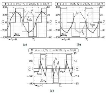
Fig. 7. Ideal voltage and current waveforms for (a) mode1+, (b) mode1−,
and (c) mode 2. The waveforms are derived using:vd c 1= 250 V,Vd c 2=
370V,L= 13μH, Lc 1 =Lc 2 = 62.1μH, n1/n2 = 1, andfs= 120kHz.
operation. These two modes are further referred to as mode 1 (high power mode) and mode 2 (low power mode) and form the basis of the final modulation schemes derived in this paper. Mode 1 can be subdivided into a submode for positive power flow [i.e., mode1+; Fig. 7(a)] and a similar submode for negative power flow [i.e., mode 1−; Fig. 7(b)], whereas mode 2 [see Fig. 7(c)] can be used for both positive and negative power flow. For the reason of clarity, below the mode equations are presented for mode1+and mode 2 only.14Nevertheless, in the
scope of the search toward optimal ZVS modulation schemes, the expressions for all 12 modes were derived and implemented. It is explained in Section IV that, considering CDCB ZVS (see Section III) or EB ZVS, full-operating-range ZVS involving smooth mode transitions cannot be achieved with the traditional implementation of the DAB converter (i.e., a DAB with a trans-former and optionally a series inductorLin the HF ac-link). To overcome this problem, an inductance can be placed in parallel with active bridge 1 (Lc1; between nodes A and B) and/or with
active bridge 2 (Lc2; between nodes Q and P), as shown in Figs. 1
and 5. These bridge-paralleled inductances, which are further referred to as commutation inductances, always have a bene-ficial contribution to the ZVS conditions due to the injection of a small reactive current15 in the respective bridge (i.e.,i
Lc1
resp.iLc2, Fig. 6)16. In the following,Lc2is implemented by the
magnetizing inductance of the transformer (Lc2=LM),
avoid-ing the increased volume and costs. Different scenarios (i.e., using zero, one, or two commutation inductances) are discussed in Section IV-B.
14Note that the equations for mode1−are similar to those of mode1+.
15The addition of commutation inductance(s) does not necessarily lead to
higher conduction losses since the freedom to optimally controlxunder ZVS conditions becomes bigger.
16Although only shown for mode1+and mode 2, commutation inductances
TABLE II
HFAC-LINKCURRENTSiL, iL c 1,ANDiL c 2FORMODE1+ANDMODE2
For the modulation parameter conventions shown in Fig. 6, the modulation parameter relations for achieving the mode 1+ and mode 2 voltage patterns (i.e., the mode boundary conditions) are
mode1+ : −τ1+πφτ2 (6)
mode2 : τ2−τ1φ0. (7)
According to Fig. 5, neglecting the transformer leakage induc-tancesLσ1andLσ2, for each mode the dynamics of the currents
iL(t), iLc1(t), andiLc2(t)can, respectively, be expressed as
diL(t) dt = vL(t) L , diLc1(t) dt = v1(t) Lc1 , anddi Lc2(t) dt = v2(t) Lc2
with vL(t) =v1(t)−v2(t). The bridge currents iH F1(t) and
iH F2(t)are calculated using
iH F1(t) =iL(t) +iLc1(t) (8) iH F2(t) =iH F2(t)· n1 n2 = iL(t)−iLc2(t) · n1 n2 . (9) Solving above equations in each interval within half the switch-ing periodTs/2, as defined in Fig. 6, under the assumption of
steady-state operation (i.e.,iL(t) =−iL(t+Ts/2);iLc1(t) = −iLc1(t+Ts/2); and iLc2(t) =−iLc2(t+Ts/2)), and
evalu-ating the resulting systems of equations yields the expressions in Table II for the HF ac-link currents at the different switching in-stancesθi={α, β, γ, andδ}17, whereθ=ωst, withωs = 2πfs,
andfsthe switching frequency.Vdc2 is the primary side referred
dc output voltage, anddthe primary side referred voltage con-version ratio:d=Vdc2 /vdc1. Currentsi1andi2can be derived
fromiH F1 andiH F2, respectively, by analyzing the conduction
states18 of the switchesS
xx. Applying (5), the expressions for
the instantaneous DAB input current iDA B1 respectively for
17αandβcorrespond with the positive rising edge of respectivelyv
1andv2
whileγandδcorrespond with the respective positive falling edges (Fig. 6).
18The conduction states can be found in [9], Fig. 4.
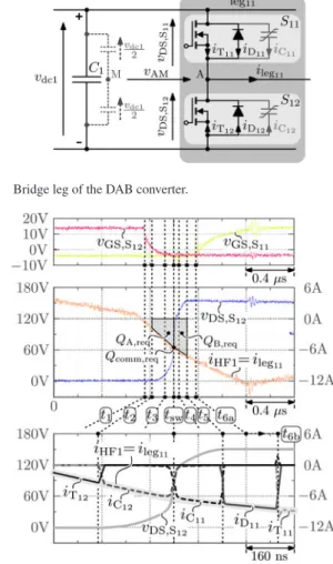
Fig. 8. Bridge leg of the DAB converter.
Fig. 9. Example of a commutation of currentile g1 1 =iH F 1from the bottom switchS1 2 to the top switchS1 1 of bridge leg1 1. The dc-bus voltage of the
bridge,vd c 1, is 150 V for this example.
mode 1+and mode 2 are
iDA B1,1+ = − Vdc2 2ωsLπ ·(φ−τ2)2+ (φ+τ1)2−τ1τ2 +π(π−2(τ1+φ))) (10) iDA B1,2 = − Vdc2 2ωsLπ· τ22−τ1τ2−2τ2φ . (11)
The DAB input powerp1(t)over one switching cycleTscan
now be calculated with
p1(t) =iDA B1(t)vdc1(t). (12)
Commutation inductances Lc1 and Lc2 do not contribute to
the power transfer and are therefore not present in any of the expressions foriDA B1andp1.
III. CURRENT-DEPENDENTCHARGE-BASED ZVS (CDCB ZVS)
The zero voltage switching (ZVS) principle is explained using Figs. 8 and 9, considering the commutation of current
ileg1 1 =iH F1 from the bottom switch S12 to the top switch
19
19The same principle applies for commutation from the top to the bottom
Fig. 10. (a) Top inset: representation of the HF high-voltage switchesSx x
(MOSFETs) of the DAB’s active bridges. Bottom inset: parasitic output ca-pacitanceCo s s(Vd s)of the used MOSFETs. (b) Charges required to achieve a
voltage change of the full dc-bus voltage (Vd c) and of half the dc-bus voltage
(VD C/2) during commutation of a bridge leg (i.e., charging/discharging of the
parasitic leg capacitanceCle g). The 150-V line corresponds with the example
in Fig. 9.
S11 of bridge leg11 (ileg1 1 is negative at the switching instant
tsw; Fig. 9). As shown in Fig. 10(a) (top inset), each switch20Sxx
consists of a power transistorTxx, a diodeDxx, and a nonlinear
parasitic capacitance Cxx (i.e.,Coss(VD S); Fig. 10(a), bottom
inset). The total parasitic leg capacitance to be considered for the commutation is highly nonlinear and can be calculated with
Cleg1 1(vA M) =C12(vD S,S1 2) +C11(vD S,S1 1) (13)
vA M(t) =vD S,S1 2(t)−
vdc1
2 (14)
vdc1 =vD S,S1 1(t) +vD S,S1 2(t). (15) The top inset of Fig. 9 depicts the measured gate voltages of the two leg switches, while the middle inset shows the measured leg currentileg1 1(=iH F1) and the measured drain-to-source volt-agevD S,S1 2 of the bottom switchS12. The simulation in Fig. 9 (bottom inset), performed using the same conditions as for the measurements, is a zoomed image (finer time scale) of the mid-dle figure inset, enabling discussion of the currents (according to Fig. 8) flowing in the individual switch components (Txx, Dxx,
andCxx).
Quasi-lossless ZVS turn-off: At time instantt1 (see Fig. 9)
the gate of switchS12, carrying a positive drain-to-source
cur-rent (iD S,S1 2(t=t1) =−iT1 2(t=t1) =−ileg1 1(t=t1)>0), is turned OFF. After a small delay (=t2−t1), the gate
thresh-old voltage is reached and the channel resistance RD S,S1 2 of
S12 starts to increase rapidly. This causes the leg currentileg1 1 to start flowing through Cleg1 1 (current divider network con-sisting ofRD S,S1 2 andCleg1 1), and in particular throughC12 [iC1 2 ≈ileg1 1, Fig. 9 (bottom inset);C12is big andC11is small at lowvD S,S1 2, Fig. 10(a) (bottom inset)]. Quasi-lossless turn-off of switchS12is achieved if the drain-source channel ofT12is
fully opened beforeileg1 1 has provided enough charge toCleg1 1 for causing a significant rise of drain-to-source voltagevD S,S1 2 (quasi-zero voltage turn-off of switchS12). This can be seen in
Fig. 9 where at time instant t3 the gate ofS12 is completely 20In this study metaloxidesemiconductor field-effect transistors (MOSFETs)
are considered.
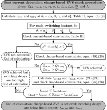
Fig. 11. Procedure to check if current-dependent charge-based (CDCB) ZVS is achieved and if the switching delays are below an upper limit.
OFF whilevD S,S1 2 is still low (C12is bypassingileg1 1, keeping
vD S,S1 2 low at turn-off).
Quasi-lossless ZVS turn-on: After time instantt2(see Fig. 9) a
resonance occurs betweenCleg1 1and the HF ac-link inductances during whichCleg1 1 is charged by ileg1 1 (t2–t5). Due to the resulting increase ofvD S,S1 2, the value ofC12 drops while that ofC11 rises, causing the leg currentileg1 1 to transfer fromC12 toC11 [aroundtsw, Fig. 9 (bottom inset)]. Att5 the resonant
transition completes (vD S,S1 2 has reached the dc-bus voltage
vdc1), putting diodeD11 into conduction. Now, transistorT11
can be turned on under (quasi) zero voltage (time instantt6;
anti-parallel diode is conducting). ZVS turn-on is thus achieved when the resonant transition (t2–t5) of drain-to-source voltage
vD S,S1 2 from ≈0 V to vdc1 completes before switch S11 is turned ON. This requires a negative leg current (i.e., into the leg) at minimum (see further).
Procedure for verifying CDCB ZVS: Based on above consid-erations a general procedure is introduced in order for a given set of input parameters (Vdc2, vdc1, τ1, τ2, φ, L, Lc1, Lc2, n1/n2
andfs) to ascertain whether quasi-lossless ZVS commutation is
achieved in all DAB bridges. Fig. 11 summarizes the complete procedure which relies on a current-dependent charge-based ZVS analysis.
Step 1: Starting from the given set of input parameters,iH F1
andiH F2at the different switching instancesθi ={α, β, γ, and
δ}are calculated using the expressions in Table II and (8)–(9). The sign of these currents is verified, keeping in mind that for the commutation from a bottom switch to a top switch of a bridge leg, the current needs to flow into the leg (charging ofCleg) and
out of the leg (discharging ofCleg) when commutation from top
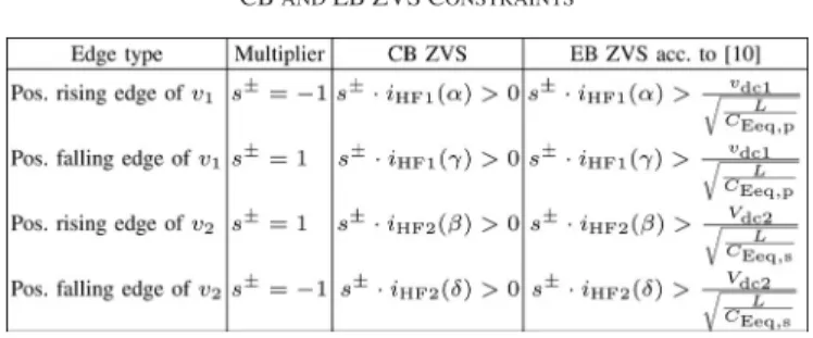
TABLE III
CBANDEB ZVS CONSTRAINTS
in Fig. 6 this yields the set of CB constraints listed in Table III (CB ZVS).
Step 2: The total charge needed to complete the commutation of a bridge leg (charging/discharging ofCleg),Qcom m,req(Vdc),
can be subdivided into chargesQA,req(Vdc)andQB,req(Vdc),
each required to achieve a voltage change of half the dc-bus voltage (VD C/2)
QA,req(Vdc) =QB,req(Vdc) =
Qcom m,req(Vdc)
2 . (16) Qcom m,req(Vdc), QA,req(Vdc), and QB,req(Vdc) for the used
MOSFETs21 are depicted in Fig. 10(b) which was obtained
using the circuit simulator GeckoCIRCUITST M [24], where a nonlinear capacitor C(u) that is based on small-signal mea-surements (such as in Fig. 10(a), bottom inset) can be directly employed [23]. Note thatQcom m,req, QA,req, andQB,reqdo not
only depend onVdc but also slightly on the leg current.
There-fore, they are derived based on an averageileg,AVG, applying
a margin (0.05μC and 0.1μC) for component variances and circuit imperfections
Qcom m,req(Vdc) =Qcom m(Vdc, ileg,AVG) + 0.1μC (17)
QA/B,req(Vdc) =QA/B(Vdc, ileg,AVG) + 0.05μC. (18)
Lossless ZVS commutation of a bridge leg occurs when the chargesQA,av andQB,av which are available in the leg-current
before (i.e.,QA,av) and after (i.e.,QB,av) the switching instant
θi are higher than or equal to, respectively,QA,req(Vdc) and
QB,req(Vdc).QA,avandQB,avare calculated using, respectively,
a backward and a forward integration of the leg current, starting atθi QA,av =s±· ⎡ ⎣ ⎛ ⎝nB j= 1 θi−j θi−j+ 1 iH F ωs dθ ⎞ ⎠+ θx θi−nB iH F ωs dθ ⎤ ⎦ QA,req (19) QB,av =s±· ⎡ ⎣ ⎛ ⎝mF j= 1 θi+j θi+j−1 −iH F ωs dθ ⎞ ⎠+ θy θi+mF −iH F ωs dθ ⎤ ⎦ QB,req (20) with:
21The FAIRCHILD FCH76N60NF SupreMOS high voltage super-junction
MOSFETs were selected for the active bridges of the final DAB converter pro-totype due to their excellent soft-switching performance, inter alia the nonlinear output capacitance, in combination with a low on-resistance.
1) θxfirst instant prior toθiwhereiH Fcrosses zero;
2) θy first instant afterθiwhereiH F crosses zero;
3) θi−j andθi+ j switching instances of the three remaining
bridges;
4) nB number of switching instances betweenθxandθi; 5) mFnumber of switching instances betweenθiandθy; 6) iH F=iH F1forθi={α, γ},iH F=iH F2forθi={β, δ}. These CDCB constraints need to be met at each switching instantθi={α, β, γ, andδ}.θx, θy, nB, andmFare calculated
using the given set of input parameters.
Step 3: In order to achieve switching at the predicted moment, the switching delaytsw,del(=tsw−t2, Fig. 9) has to be
dynam-ically compensated in the controller. Moreover, a dynamic dead-time (tdead) adaptation is required for each bridge leg, avoiding
back commutation. At each switching instant θi, tsw,del and
tdeadare, respectively, calculated as
tsw,del= θi−θA ωs (21) tdead= θB−θA ωs (22) where θA andθB are the instances where the backward and
forward integration [(19) and (20); starting pointθi] of the cor-responding leg current equals the charge needed to achieve a voltage change of half the dc-bus voltage (Vdc/2).θA andθB
are found by, respectively, solving
s±· θA θi iH F ωs dθ=QA,req (23) s±· θB θi −iH F ωs dθ=QB,req. (24)
Step 4: Finally, it is verified if tsw,del and (tdead−tsw,del)
are smaller than an upper limit, avoiding too long commutation delays. This yields a set of time-based constraints22
tsw,del tsw,del,m ax (25)
tdead−tsw,del (tdead−tsw,del)m ax. (26)
The error due to the linear approximation of the HF ac-link currents is small as, due to the strong nonlinearity of the leg capacitances, the energy transfer to and from the capacitances during commutation is almost fully concentrated in time inter-valst2–t3andt4–t5(see Fig. 9). During these intervalsvD S,S1 2 remains quasi-constant. Therefore, the momentaneous resonant transition has a negligible influence on the linear shape of the HF ac-link currents (see Figs. 9 and 21) and the expressions in Table II are still valid. Qausi simultaneously with this study, a similar charge-based ZVS analysis for a TCM PFC rectifier has been proposed in [25], strengthening the validity.
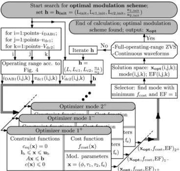
IV. OPTIMALMODULATIONSCHEMES
For determining an optimal modulation scheme for the DAB an optimization algorithm is proposed which is based on a
Fig. 12. Procedure to determine an optimal modulation scheme and the opti-mal modulation parametersxo p t, using a constrained numerical optimization. constrained numerical minimum search (i.e., a constrained non-linear optimization23). Closed form solutions, such as
pre-sented in [12], for the optimal modulation parametersxopt= (φopt, τ1,opt, τ2,opt, fs,opt)are not directly feasible because of
the three following reasons:
1) User definability of the cost-functionfcost(x): according
to their needs, users can predefine a cost function to be minimized. This allows us to include all converter related losses, but also requirements concerning system volume, weight, control, EMI,. . .A closed form solution forxopt
would require a fixed cost function.
2) Discontinuity of the ZVS conditions: the CDCB ZVS cri-terion (see Section III) introduces discontinuities [i.e.,
0nB, mF3, (19), (20)] in the constraints for ZVS,
as well as additional boundaries due to the time-based constraints [(25), (26)].
3) Increased complexity: additional terms appear in the “mode equations” (see Section II-C) due to the inclusion of commutation inductances (Lc1 and Lc2). Moreover,
the use of a variable switching frequency adds a degree of freedom to modulate the active bridges of the DAB. Fig. 12 summarizes the optimization procedure which starts from an initial set of circuit level variables h=
hinit=(Linit, Lc1,init, Lc2,init, and n1,init/n2,init). Then, it
iterates through the operating range, passing variables
iDA B1(i, j, k), vdc1(i, j, k), Vdc2(i, j, k), andhto the core
al-gorithm. Here, for each switching mode an optimizer is applied to find the minimum of a cost functionfcost(x), while satisfying
the constraint functions for that mode. The results (xopt, fcost,
and exitflag EF) from each mode optimizer are inputted to a
23The final algorithm was implemented in MATLABT Musing the
‘fmincon’-function of the Optimization ToolboxT M, and verified using a Genetic
Algo-rithm of the Global Optimization ToolboxT M.
selector for detecting which mode satisfies the constraint func-tions (i.e., exit flag EF= 1) and has the “best value” for the cost function, outputtingxopt(i, j, k),mode(i, j, k), and EF(i, j, k). The circuit level variablesh= (L, Lc1, Lc2,andn1/n2)are
var-ied in a top level iteration loop until full-operating-range ZVS is achieved (i.e., all EF= 1), and until the resulting solution is continuous (no discontinuous steps in xopt), yielding the
optimal modulation scheme.
A. Implementation of the Constrained Nonlinear Optimization First, for each mode the constraint functions and the cost functionfcost(x)need to be defined.
1) Constraint Functions: These can be subdivided into: 1) functions describing the relationiDA B1 =f(x); e.g. (10)–
(11). These are nonlinear and can be rewritten to subject the optimizer to nonlinear equalityceq(x) = 0;
2) functions describing the physical limitations onx (e.g.,
0τ1 πandfs,m infsfs,m ax). This yields a set
of lower and upper bounds so that the solution of the optimization is always in the rangelbxub;
3) functions describing the mode boundaries [e.g., (6)-(7)], assuring that the resultingxopt for a certain mode does
not result in a different mode of operation. These can be written as a set of linear inequalities,Axb;
4) functions describing the ZVS24 boundaries according to Section III (19)–(26) and Fig. 11. These can be written as nonlinear inequalitiesc(x)0.
2) Cost Functionfcost(x): For investigations of the DAB
topology, most often converter losses are chosen forfcost(x),
and the impact of HF losses caused by current harmonics is neglected in a first design phase [12], [17]. According to [11], [12], under ZVS operation, the transistor’s conduction losses account for the biggest part (>50%) of the total converter losses. For this reason, only the DAB MOSFET conduction losses are considered for illustrating the optimization procedure proposed in this paper (similar to [12]). These are proportional to(I2
H F1+
I2
H F2)as both active bridges use the same type of MOSFETs,
yielding
fcost(x) = (IH F12 +IH F22 ). (27)
3) Switching Frequency Range: An upper limit offs,m ax =
120 kHz was selected to accommodate a compact converter design without causing excessive switching frequency related losses such as conduction losses due to high-frequency effects, core losses, and switching losses. Moreover, thermal limitations apply at high-switching frequencies, resulting in an increased total converter volume.fs,m ax was chosen to stay well below
these thermal limits. The choice offs,m in is based on design
considerations related to the DM EMC input filter which is designed according to [26] and [27] for compliance to CISPR 22 Class B in the frequency range of 150 kHz – 30 MHz. A two-stage DM filter with optimized damping is selected (see Fig. 2, Table IV).fs,m in = 75kHz, which is doubled toward 24The DAB operation is assumed/recommended to be, but not limited to
ZVS. Alternatively hard-switching operation could be allowed and the switching losses could be included in the cost function.
TABLE IV
COMPONENTVALUES OF THEDM EMC FILTER
the input port of the DAB converter, is chosen so that2·fs,m in
is well beyond the maximum second filter cut-off frequency, assuring enough margin to attenuate the lower HF harmonics of the input current. However, for an optimal DM filter design it might be advantageous to selectfs,m in higher than 75 kHz,
en-abling higher filter cut-off frequencies [28]. Allowing a variable switching frequency has the same effect as changing the induc-tance values. Therefore, investigations with other inducinduc-tances are implicitly covered.
4) Circuit Level Variablesh: For allowing a clear compari-son of the different scenarios discussed in Section IV-B,n1/n2
andLare taken the same for each scenario:
Transformer’s turns ratio: n1/n2 is determined such
thatVdc2 ,m in >(ˆvdc1,m ax+ 10Vmargin)is always satisfied.25
Given the specifications in Table I, withVdc2 ,m in = 370V (min-imum primary side referred output voltage) and vˆdc1,m ax =
358 V (maximum DAB input voltage), a ratio ofn1/n2 = 1
is chosen. Note that the valley inVdc2 , due to the 100-Hz volt-age ripple occurs 45◦out of phase withvˆdc1.
Main inductanceL: The maximum positive DAB input cur-rent26 iDA B1,m ax is achieved atτ1 =τ2 =π;φ=π/2; mode
1+ [12], and needs to be higher than the maximum required DAB input current according to (4)
iDA B1,m ax = Vdc2nn12 8fsL (max(iDA B1,u) = 24A). (28)
The upper limit ofLcan be calculated with (28) by setting
fs =fs,m ax = 120kHz,Vdc2=Vdc2,m in = 370V,n1/n2= 1,
yieldingLm ax= 16.06μH. A good choice is to takeLinit ≈
(0.75. . .0.85)·Lm ax, i.e., leaving some margin to optimally
modulate x. The final value, L= 13μH, is the result of an iteration performed during the converter’s design phase. B. Results of the Numerical Optimizations
The search toward optimal modulation parametersxopt
us-ing the proposed optimization procedure (see Fig. 12) is illus-trated for different scenarios concerning commutation induc-tances (Lc1 and Lc2) and ZVS conditions. For each scenario xoptis calculated for the whole DAB operating range according
to Fig. 4, applying 75kHzfs 120kHz, n1/n2= 1, and
25The DAB can also be operated with other settings (e.g., allowing
Vd c 2 ,m inˆvd c 1,m a x) [12]. For the 1-S DAB ac–dc converter, operated under
variabled, this implies crossing ofd= 1. However, in the vicinity ofd= 1, CDCB ZVS is hard to obtain as the inductor volt-seconds product needed to achieve the required current crossing in intervalβ−δ(Fig. 6(b); low power mode) is too small. Low inductance values forLc 1and/orLc 2would be needed,
leading to increased rms values of the HF ac-link currents.
26For maximum negative current:τ
1 =τ2=π;φ=π/2; mode 1−; this
yields an equation similar to (28).
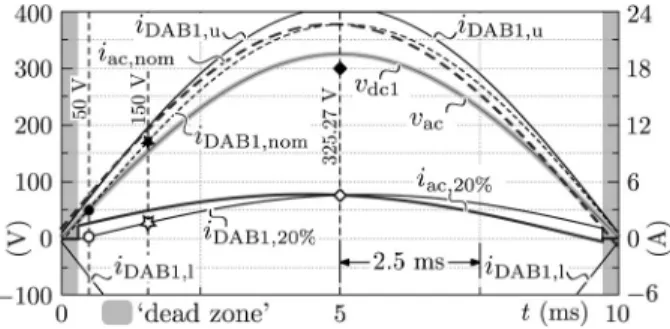
Fig. 13. DAB input currents iD A B 1, required to achieve Ia c,P=
Ia c,P,n o m = 16Arm s; PF= 0.999,respectively,Ia c,P= 0.2·Ia c,P,n o m=
3.2Arm s; PF= 0.983. Here,Va c = 230Vrm s (nominal ac input voltage).
Vertical dashed lines:vd c 1={50 V;150 V; 325.27V}.
L= 13μH (cf. Section IV-A). Remind that the optimizer out-putsxopt. Other quantities (graphs below) are calculated using
xopt in the analytical models of Section II.
1) Scenario 1, no Use of Commutation Inductances (Infinite
Lc1; InfiniteLc2): This is the way the DAB converter is
tradi-tionally implemented: iLc1(t) =iLc2(t) = 0; iH F1(t) =iL(t)
according to (8);iH F2(t) =iL(t)·n1/n2 according to (9); no
injection of additional reactive currents in the active bridges of the DAB.
1st run: Illustratively the optimization is performed a first
time applying the theoretical CB ZVS constraints (see Table III). In Fig. 14, the results forτ2,opt[see Fig. 14(a)] andfs,opt[see
Fig. 14(b)] at an output voltage ofVdc2 = 400V are given as
an example. Although the CB ZVS conditions are met within the whole operating range, the CDCB ZVS conditions (see Section III) are mostly violated as indicated by the ZVS ar-eas in Fig. 14(c). The same goes for the EB ZVS constraints given in [10] (listed in Table III, EB ZVS). In Fig. 16(a) and (b), the trajectories (solid lines) of, respectively, the modula-tion angles and the switching frequency are depicted which are run through during a half-cycle of the nominal ac in-put voltage (Vac= 230 Vrm s) at the nominal input current of
Iac,P =Iac,P,nom = 16Arm sand a power factor of PF= 0.999
(according to Fig. 13). Fig. 16(c) and (d) (solid lines) show
s±·iH F1(α) and s±·iH F1(γ), respectively s±·iH F2(β) and
s±·iH F2(δ)which clearly satisfy the CB ZVS constraints (i.e.
they need to be bigger than zero). However, they are below the limit for EB ZVS (according to [10]) during the major part of the half cycle. The same goes for the commutation charges27 which do not reach the CDCB ZVS limit [according to equa-tions (19), (20)], as shown in Fig. 16(e) and (f) (solid lines). The solution for xopt is similar to the one presented in [12],
val-idating the optimization algorithm. As expected, only mode 1 (low power mode) and mode 2 (high power mode) are used [see Fig. 16(a)]. Moreover, the modulation parameter trajectories are continuous.
2ndrun: A second optimization is performed using the same
conditions as in the first run, with the difference that now the optimizer is subjected to the CDCB ZVS constraints proposed in this paper (see Section III). From Fig. 15, it can be seen
27For convenience onlyQ
A ,av andQB,avfor commutation instancesθi=
Fig. 14. Results of the numerical search for optimal modulation schemes according to scenario 1 (1s trun): no use of commutation inductances (Lc1 =Lc2 =∞). The optimizer is subjected to the CB ZVS conditions, using all possible modes. The output voltage for this example isVd c 2 = 400V.
Fig. 15. Results of the numerical search for optimal modulation schemes according to scenario 1 (2n drun): no use of commutation inductances (Lc1 =Lc2 =
∞). The optimizer is subjected to the CDCB ZVS conditions, using mode 1 and mode 2 only. The output voltage for this example isVd c 2= 400V.
Fig. 16. AC trajectories for achievingIa c,P =Ia c,P,n o m= 16Arm s, and PF= 0.999, atVd c 2 = 400V (half cycle of the nominal ac input voltageVa c= 230
Vrm s; according to Fig. 13). Solid lines: conditions cf. scenario 1,1s trun (all modes included). Dot dashed lines: conditions cf. scenario 1,2n d run (all modes
included).
that there are regions in the operating range (especially along the mode boundary and at low vdc1) where the CDCB ZVS
conditions cannot be met. Note that for the results in this figure, only mode 1 and mode 2 are used in the optimizer. In Fig. 16 (dot dashed lines), using all possible modes in the optimizer, these region are now covered by a very inefficient mode 3, resulting in full-operating-range CDCB ZVS [see Figs. 16(e)
and (f)]. However, highly discontinuous modulation parameter trajectories and inefficient operation are obtained. It is a clear indication that it is impossible to achieve “efficient” (i.e., mode 1 and 2 only) full-operating-range CDCB ZVS with the traditional DAB (i.e., withoutLc1andLc2).
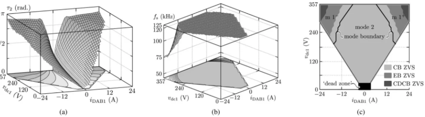
2) Scenario 2, Primary and Secondary Side Commutation Inductances (FniteLc1; FniteLc2): As proposed in this paper,
Fig. 17. Results of the numerical search for optimal modulation schemes according to scenario 2: primary and secondary side commutation inductances (Lc1 =Lc2 = 62.1μH). The optimizer is subjected to the CDCB ZVS conditions, using all possible modes and an output voltage ofVd c 2=Vd c 2,m in= 370V.
Fig. 18. AC trajectories for achievingIa c,P=Ia c,P,n o m = 16Arm s,PF= 0.999(dot dashed lines), andIa c,P = 0.2·Ia c,P,n o m= 3.2Arm s,PF= 0.983
(solid lines), atVd c 2 =Vd c 2,m in= 370V (half-cycle of the nominal ac input voltageVa c = 230Vrm s; according to Fig. 13). Conditions cf. scenario 2 (all
modes included). Vertical dashed lines:vd c 1={50 V;150 V; 325.27V}cf. Fig. 13.
the DAB is now implemented with finite Lc1 and Lc2, and
the optimization (including all possible modes) is performed applying the CDCB ZVS constraints (see Section III). Equal commutation inductances are assumed, which are top-level-iterated until full-operating-range ZVS under the efficient modes 1 and 2 is achieved, yielding (Lc1=Lc2 = 62.1μH). The
re-sults for the worst case output voltageVdc2 =Vdc2,m in = 370V
and the nominal ac input voltageVac= 230 Vrm s are shown
in Figs. 17 (full operating range) and 18 (ac trajectories for
Iac,P =Iac,P,nom = 16 Arm s; PF= 0.999; dot dashed lines,
and forIac,P = 0.2·Iac,P,nom = 3.2Arm s; PF= 0.983; solid
lines). Full-operating-range CDCB ZVS is achieved under efficient modes 1 and 2 only, while the modulation parame-ter trajectories are continuous. Similar results can be obtained using only one commutation inductance (i.e., finite Lc1,
in-finite Lc2 or infinite Lc1, finite Lc2), which however yield
more unbalanced HF ac-link current values. The case with infi-niteLc1, finiteLc2for example would requireLc2 = 29.7μH.
Fig. 19. 3.7 kW, single-phase, single-stage, bidirectional and isolated DAB ac–dc converter prototype (177 mm×130 mm×72 mm).
Measurements of the HF ac-link voltage and current patterns at different points of the ac-trajectories are shown in Fig. 21 and briefly discussed in Section V-B1. There it is also explained how these measurements can be validated by comparing the cur-rent values at the diffecur-rent switching instances in Fig. 21 with the values on the trajectories shown in Fig. 18(c) and (d). To-gether with Fig. 18(a) and (b) this gives a clear view on how the modulation angles, the frequency, the modes,. . ., evolve during sinusoidal operation.
V. EXPERIMENTALRESULTS
The experimental results are obtained from the DAB ac–dc hardware prototype depicted in Fig. 19, which is designed ac-cording to the specifications given in Table I. Providing detailed information about the design of each subcomponent is for the reason of clarity not within the scope of this paper. In fact, the final prototype is designed using a recursive design procedure. The basic technical data of the system are:
1) power PCB’s: 2-layers, 105μm copper per layer; auxiliary and other PCB’s: 4-layers, 35μm copper per layer; 2) HF DAB switches: FCH76N60NF (SupreMOST M); 3) SR switches: STY112N65M5 (PowerMESHT M);
4) HF caps.C2: 7×1.5μF/630 Vdcin parallel (MKP);
5) HF caps.C1: 6×2.2μF/305 Vac/X2 in parallel (MKP);
6) LF caps.C2,st: 3×390μF/500 Vdc in parallel (ELCO);
7) transformer: turns ratio n1/n2 = 1, N97 core material,
2×2 planar ELP58 cores, magnetizing inductance (i.e., commutation inductanceLc2)Lc2=LM = 62.1μH
(us-ing an airgap), Litz wire;
8) main inductor:L= 13μH, N97 core material, 3×2 pla-nar ELP38 cores, Litz wire;
9) commutation inductanceLc1= 62.1μH, N97 core
mate-rial, 1×2 planar ELP58 cores, Litz wire; 10) DM EMC filter: see Table IV and Fig. 2; 11) CM EMC filter: out of the scope of this paper.
It should be noted that the primary side commutation induc-tanceLc1was originally not included in the hardware design,
but added in a later phase in order to achieve full-operating-range CDCB ZVS according to the analysis given in this paper. Although not shown in Fig. 19, during testing it was connected to the hardware with the screws that are located on the top power
TABLE V
PROTOTYPEPOWERDENSITYVALUES(AT3.7KW NOMINALPOWER)
PCB (i.e., using the connection points of the transformer and inductorL). Also, the volume of this inductor is included in the results for the system’s power density, which are listed in Table V. As a consequence, a further design iteration with opti-mized ac-link would certainly yield even higher efficiencies and power densities than presented below.
A. Practical Implementation of the Controller
1) Controller Hardware: The control hardware con-sists of an on-board FPGA, in particular the ALTERA EP3C25E144C8N CYCLONE III, which is operated with a clock frequency of 62.5 MHz and programmed in the VHDL hardware description language. The FPGA is responsible for generating the PWM gate drive signals, for reading in the cur-rent and voltage measurement peripherals (A/D converters), and for “fast” overcurrent and overvoltage protection. More-over, it communicates over Ethernet with an off-board PC-based real-time target (RTT) from Triphase [29].28 The RTT can be programmed and operated through MATLAB/Simulink, where the controllers, the “slow” protection, the start-stop pro-cedures, the control parameter generation, and the delay and dead-time compensation are implemented (see Section V-A2). The Real-TimeWorkshop automatic code generator translates the MATLAB/Simulink model into C-code which is compiled and executed by the RTT.
2) Controller Software: The cascaded control structure used to control the DAB input currentiDA B1in accordance to (2) is
shown in Fig. 20. The dashed lines indicate which part of the controller hardware (see Section V-A1) performs each particular task. The measured quantities (index m) that are available in the PFGA as digital signals are also indicated in Fig. 20. A PI current control loop controlsiDA B1based on a reference valueiDA B1,ref
which is generated using a phase locked loop and calculation of (2). The set valuesIˆac∗,P, dir∗, and PF∗origin from an external source such as the battery management system or the vehicle power management system. For testing of the prototype system, a fixed voltage was used at the output of the DAB and the set values were manually applied. Optionally, an outer PI voltage controller can be used to control the output voltageVdc2.
The control parameters needed for the DAB to generate the set currentiDA B1,setare determined using lookup tables which
are calculated for the whole converter’s operating range, as ex-plained in Section IV. Based on[iDA B1,set;vdc1,m;Vdc2,m], the
modulation parametersxset, the delay vectortsw,del,set, and
the dead time vectortdead,set are determined using linear
ta-ble interpolation.tsw,del,set and tdead,set consist of
respec-tively the switching delaystsw,del(21) and dead timestdead,m in 28The use of the Triphase RTT allows flexible implementation of different
control algorithms. In a next phase the functions of the RTT can be implemented on the 3C25 FPGA by means of an embedded CPU [29].
Fig. 20. Control structure employed to control the input current iD A B 1 in accordance to (2) as well as the modulator function, the SR switch, and the
enabling/disabling units (i.e. the start/stop/runtime, overcurrrent and overvoltage protection, and boundary check). The dashed lines indicate which part of the controller hardware (RRT, FPGA, or power stage/measurements) performs each particular task.
Fig. 21. Measured HF ac-link currents/voltages at six different points of the ac trajectories in Fig. 13 (Vd c 2=Vd c 2,m in= 370V: i.e. the, for ZVS, worst case
output voltage). The top inset of each subfigure contains the DAB primary side currents, and the bottom inset the DAB secondary side currents. (22) at the different commutation instances θi={α, β, γ,
and δ}. Finally, the modulator function calculates the fre-quency counter fctr, and the timing and duty-cycle counters
for each bridge leg: Tctr = [Tctr,11;Tctr,12;Tctr,21;Tctr,22]; Dctr = [Dctr,11;Dctr,12;Dctr,21;Dctr,22]. These, as well as the
enable signalsENand the SR statestSR, are inputted to the
FPGA PWM-generation modules.
B. Measurements
Below, the results of a dc–dc and ac–dc characterization of the prototype system at room temperature (TA = 22◦C) are
presented. Although the power supply did not allow to sink power, and therefore only positive power flow could be applied, the results for negative power flow would be similar as the DAB is completely symmetric. The conversion efficiency is evaluated
Fig. 22. Measured waveforms in ac–dc operation at different input currents and output voltages, and at the nominal ac input voltageVa c= 230Vrm s.
using the Yokogawa WT3000 precision power analyzer, having a power accuracy reading of±0.02%.
1) DC–DC Operation: A first prototype characterization is performed applying dc voltages at both the input (ac-side) and at the output (dc-side) terminals of the ac–dc converter. Fig. 21 shows the HF ac-link currents and voltages at six different points of the ac trajectories depicted in Figs. 13 and 18 (i.e., cf. scenario 2, Section IV-B2). A subfigure in Fig. 21 and its corresponding point in Fig. 13 are equally marked. For each voltagevdc1 = {50V; 150V; 325.27V}(vertical dashed lines in Figs. 13 and 18) two different points (one on the lineIac,P =Iac,P,nom = 16
Arm s, and one on the lineIac,P = 0.2·Iac,P,nom = 3.2Arm s)
are captured. Forvdc1 = 325.27V, the point on the lineIac,P =
Iac,P,nom = 16Arm sis not measured as here the power transfer
would be as high as 7.4 kW. In continuous dc–dc operation this would cause an overtemperature, and thereforeiDA B1is limited
to 18 A [Figs. 13 and 21(f)]. The values of the HF-link currents (iH F1andiH F2) at the different switching instantsθi={α, β, γ, andδ}in Fig. 21 show very good agreement with the calculated values in Fig. 18(c) and (d). The same goes for the modulation angles and the switching frequency, validating the CDCB ZVS analysis method and practical implementation of the strategy. Additionally CDCB ZVS operation was successfully verified by visual inspection of the waveforms, according to Section III.
Fig. 23. Measured efficiency, THD, and (true) PF in ac–dc operation. Mea-surements are taken at the nominal ac input voltageVa c= 230Vrm s, in the
whole power range and at different output voltages.
Also remind that here the, for ZVS, worst case output voltage
Vdc2 =Vdc2,m in = 370V is applied.
2) AC–DC Operation: For the ac–dc characterization the nominal ac input voltageVac= 230Vrm sis provided to the input
(ac-side) of the converter by an ac power source, while the output (dc-side) is connected to a 5.9 mF dc-bus and a load. Fig. 22 depicts the measured waveforms at different input currents and output voltages. Note that the maximum output voltage that could be applied with the measurement setup isVdc2 = 450V.
The system was successfully tested in the full power range (up until an output power of 3.7 kW), showing waveforms with little distortion [see Fig. 22 and Fig. 23 (bottom inset, THD)], a (true) PF close to unity [see Fig. 23 (bottom inset, PF)], and a high conversion efficiency in the whole power and output voltage range [see Fig. 23 (top inset)]. The latter is measured including and excluding auxiliary (i.e., gate drivers, fans, and control board) losses. An improved THD would be achieved by replacement of the on-board sample-based measurements circuits by Delta-Sigma measurements. Moreover, optimization of the ac-link components would yield even higher efficiencies.
3) Further Remarks on the Practical Realization: The closed-loop control of DAB converters is typically performed using lookup tables in which precalculated values for the mod-ulation parameters (i.e., the duty-cycles, the phase-shift angle, the dead-times, and the delay compensation) are stored. How-ever, table entries are dedicated results for one particular DAB converter. In practice, the system may be sensitive to changes of inductance values, and care should be taken when using high-performance MOSFET’s. Loss of ZVS can easily cause device destruction. The DAB inductances, however, could be consid-ered as another dimension of the lookup table.
Due to the presence of an SR, the investigated ac–dc con-verter might be identified as a “quasi” single-stage concon-verter rather than a “single-stage” converter. However, alternatively the SR can be integrated in the primary side active bridge of the