Modeling CNT Interfaces Using NEGF Approach
Amardeep, Nisha,Vijay kr. LambaAbstract: In this work we used SWCNT and GNRs, for the purpose of studying their applications as a nanoscale sensors. We assumed in this work that, under the simulated conditions, inelastic scattering processes were negligible and we were dealing with an effectively ballistic transport regime. The observations discussed above revealed the potential applications of carbon nano tube for measuring stress and temperature as well as in SWCNT can be used for wide range applications in design of a versatile nanoscale sensor.
————————————————————
1.
INTRODUCTION
Material scientists are using various allotropic form of Carbon to propose and design organic devices to make devices flexible in nature and as an alternative of silicon based technology. Since conventional technology involves lengthy fabrication steps using top-down approach, further scaling of devices will soon reach their limit [1-3]; therefore, it is need of time to explore new processes and materials. The carbon-based systems because of its bounding properties (catenation), it shows an unlimited number of different structures with different physical as well as electronics properties. Further creating and calibrating transport through molecular junction has become a vital task to carry out research in this field [1-6]. The transport characteristics across a molecular junction are controlled by intrinsic properties of the molecule, the contacts, and the electrode. Hence understanding, modeling and stimulating the charge transport properties for molecular devices is the crucial need of the hour [7-11]. This is because molecules have both ultra-small dimensions and a overwhelming degree of diversity and functionality. This makes it important to explore alternatives to conceptualize new device structures and for this new approach is needed to understand mechanism of charge transport in molecular devices. These materials such as carbon nanotubes (CNT) and graphene have offered a vast potential for presenting next-generation material for diverse applications such as field emission, electronics, sensors and energy [16-21], because they posses excellent carrier mobility (e.g. ballistic conduction) with much lower thermal and electrical noises [22-23]. In this paper, we tried to find out the effect of change in CNT configuration on electronic properties of nano junctions. We further studied the effect of metal molecule interaction on device configuration using homogeneous and heterogeneous electrode configuration.
METHOD
We used the real-space nonequilibrium Green‘s function (NEGF) method in combination of DFT and EHT to realize the simulation of electronic or spin-polarized quantum transport [24-25] . We further used tight binding Extended Huckle Theory (EHT) [26-29] in device mode, being a semi-empirical approach, the results obtained shows similar trends with experimental techniques. We consider that the effect of inelastic scattering is negligible, and assumes that
whole simulation works in effectively ballistic transport regime. Further for simplification we used single-particle approach, further we considered cerda- Huckle parameters [30-34] to introduce real time scattering effects. Initially we computed have used (4, 0), (5, 0) & (7, 0) SWCNT configured to form device shown in figure 1. We studied the electron transport under the different bias conditions.
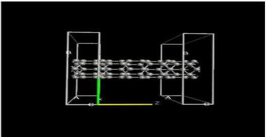
Figure 1: (5, 0) CNT device model coupled to electrodes in ATK builder
For our modelled of CNT device structure as shown in figure 1 using two probe system, and geometry optimization is performed using guassian. 25% of the length of the electrodes (0.71043 Å) was considered as the extended central molecule along with the carbon nano tube in order to compensate for the scattering losses at the interfaces of the central molecule and the left-right electrodes. The grid cut-off was considered to be 100 Hartrees, while k-point sampling was taken (5,5,100) for the calculation to be optimal combination of accuracy and speed. The electron temperature was set at 273 K, before the geometry optimization was done. We varied the applied bias across the two electrodes in the range of -2 Volt to 2 Volt in the steps of 0.25 V and measured the effective variation in the value of stress. Next we transmuted the bond length of the carbon-carbon bond to predict the change in the value of stress. Finally the rotation of the Molecule was considered in various axes to monitor the effective changes in stress due to this these geometric variations. We modeled the transport characteristics like I-V curves, Conductance curve through the SWCNT under contrasting temperature conditions to establish our objectives of SWCNT as a versatile sensor.
RESULTS AND DISCUSSION
The modelled (4,0), (5,0) and (6,0) SWCNT under varying applied bias and measured the resultant change in the values of the stress. By scrutinizing these values and
————————————————
Amardeep is currently pursuing PhD in Electronics Engineering, in IKGPTU Jalandhar, India, E-mail: [email protected] Nisha is currently pursuing PhD in Electronics Engineering, in
IKGPTU Jalandhar, India, E-mail: [email protected] Vijay Kumar Lamba is faculty at GCET Kahnpur Khui, India,
plotting, we observed that the nature of stress was compressive as shown in figure 2. This compressive stress varied linearly as the bias changed from -1 V to -0.25 V and remained constant for the bias voltages between -0.25 V to 0.75 V before rising linearly to settle for 1 V external bias. As Young modulus is directly proportional to stress, the observed results depicted the variation of Young‘s modulus for (4,0), (5,0) and (6,0) CNT with changes in applied external voltage.
Figure 2: Applied Bias Vs. Stress
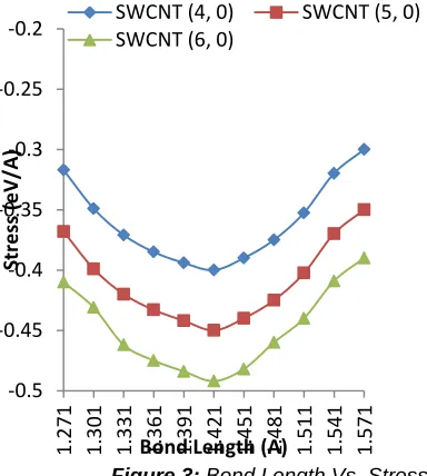
Next we transmuted the bond length of the C-C bond to measure the impact of this change on the overall transport behaviour and the stress. We observed from the figure 3 that as the bond length of the C-C bond was increased from the default value of 1.42086 Å to the maximum value of 1.69 Å (after that C-C bond breaks and structure geometry disrupted), it means that there was less stress on the CNT as we increased the bond length in discrete steps.
Figure 3: Bond Length Vs. Stress
At the end we observed that there was the increased conductance as we raised the electron temperature from 250K onwards upto 300K and the reported values of conductance are shown in figure. The conductivity increased exponentially as we moved away from the room temperature regime as shown in figure 4. The substantial change in the overall conductivity of the CNT with temperature made us think about developing CNT based temperature sensor.
Figure 4: Conductance Vs. Electron Temperature plot
Further we used SIESTA to analyze HOMO- LUMO gap of molecular system we designed (figure 5). Rotation of sandwiched layer
Fig. 5: Device configuration used for simulation -0.396
-0.395 -0.394 -0.393 -0.392 -0.391 -0.39
-1 -0.75 -0.5 -0.25 0 0.25 0.5 0.75 1
Str
e
ss (e
V/
A
n
g)
Applied Bias (Volts)
SWCNT (4,0) SWCNT (5,0)
-0.5 -0.45 -0.4 -0.35 -0.3 -0.25 -0.2
1.2
71
1.3
01
1.3
31
1.3
61
1.3
91
1.4
21
1.4
51
1.4
81
1.5
11
1.5
41
1.5
71
Str
e
ss (e
V/
A
)
Bond Length (A)
SWCNT (4, 0) SWCNT (5, 0)
SWCNT (6, 0)
0 0.05 0.1 0.15 0.2 0.25
250 255 260 265 270 275 280 285 290 295 300
Co
n
d
u
ctan
ce
(n
S)
Electron Temperature (K)
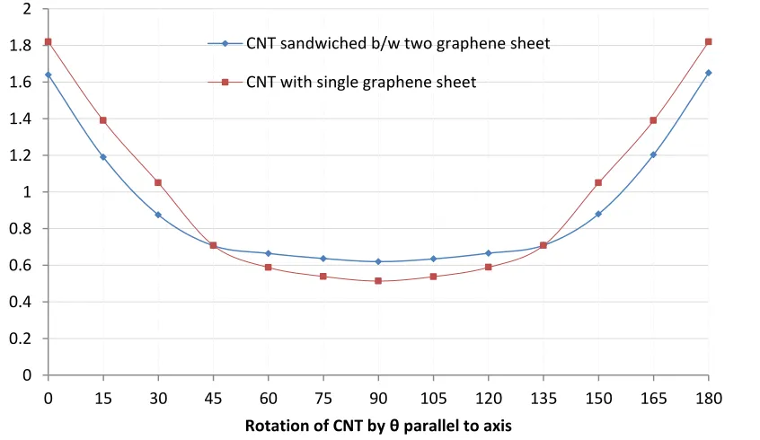
Fig. 6: With the change of rotation angle θ between CNT and graphene sheet,the value of HOMO-LUMO gap initially reduces exponentially.
of CNT (4,0) plays an significant responsibility in electronic transport for the reason that molecular levels shifts and expands spectacularly and results reflected as change in the HOMO-LUMO gap due to its dissimilar electronic conifigration. Due to the rotation processes the disconnected molecular levels expends up resulting in a spectrum continous in nature for density of states. The disparity in HOMO-LUMO gaps with the molecular rotation
will decide the angle dependence of conductance. As a result of rotation of the molecule along z axis, the gap between HOMO-LUMO level dwindles up and produces complex overlapping of the tails of HOMO and LUMO take place making it hefty, resulting in the increase of transmission coefficient around Fermi level EF resulting
increase in conductance value.
Figure 7: Change in conductance when CNT is rotated parallel to axis. 0
0.5 1 1.5 2 2.5 3
0 15 30 45 60 75 90 105 120 135 150 165 180
H
OM
O
-LU
M
O
gap
(e
V)
Rotation of CNTby θ parallel to axis
CNT sandwiched b/w two graphene sheet
CNT with single grapheen sheet
0 0.2 0.4 0.6 0.8 1 1.2 1.4 1.6 1.8 2
0 15 30 45 60 75 90 105 120 135 150 165 180
Co
n
d
u
ctan
ce
(In
Go
)
Rotation of CNT by θ parallel to axis
CNT sandwiched b/w two graphene sheet
When the molecule-electrode distance and electronic structure of the molecule does not transform appreciably than the processes of wrapping up is only applicable while its point of reference is being changed. In present case benzene molecule is rotated about the bottom ‗‗atom‘‘ and therefor it modify the angle θ between the main axis of the modeled system and the surface normal to it since it is sandwiched between electrodes along the z axis resulting
the change in angle θ, there for the p orbitals linger around the molecular ‗‗backbone‘‘ slanting perpendicular to it. Since the surfaces of the two electrodes always hang about parallel, to each other and molecule-electrode bond lengths do not modify with θ, there for the distance between LUMO and HOMO is given by the relation ELUMO – EHOMO = 2tπ
(were tπ gives hopping distance between the π orbitals).
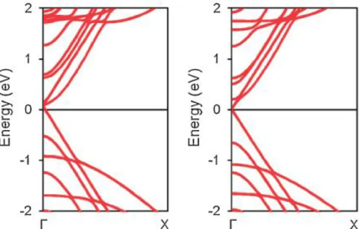
Fig. 8. Energy band structures for the periodic structures of the contact area in the models at 0o. (a) is for Models 1 and (b) is for Models 2
The central point of the gap is associated with the chemical potential of the electoder at zero bias voltage (V = 0). Thus from the fig. 6 & 7 & 8 we conclude the as we rotate CNT conductance increases initially and then decreases and pattern is repeated. So we can use such a system to design sensors for measuring mechanical properties of polymers and molecular wires/rods.
CONCLUSIONS
Through this work with SWCNT and Crossed junctions of GNRs, deviced for the purpose of studying their applications as a nanoscale sensors. We assumed in this work that, under the simulated conditions, inelastic scattering processes were negligible and we were dealing with an effectively ballistic transport regime. The observations discussed above revealed the potential applications of carbon nano tube for measuring stress and temperature as well as in SWCNT can be used for wide range applications in design of a versatile nanoscale sensor.
REFERENCES:
[1] The International Technology Roadmap for Semiconductors (ITRS), Chapter 1 & 11, (2008) http://www.itrs.net/Links/2008ITRS/Home2008.htm) [2] M. Lundstrom ―Moore‘s law forever? Science, Vol.
299(210 -211)
[3] Venugopal,R., Ren, Z. ; Datta, S. ; Lundstrom, M.S. ; Jovanovic, D., ―Simulating quantum transport in nanoscale transistors: Real versus mode-space
approaches‖ Journal of Applied Physics, volume 92( 3730),2002.
[4] Lundstrom Mark, Zhibin Ren, ―Essential physics of carrier transport in nanoscale MOSFETs‖ IEEE Transactions on Electron Devices, Vol. 49(133-141),2002.
[5] Chen, Z., Appenzeller, J., Knoch, J., Lin, Y. M. and Avouris, P., ―The role of metal–nanotube contact in the performance of carbon nanotube field-effect transistors‖, Nano Lett., Vol. 5(1497–1502) 2005. [6] P.R. Wallace , ―The Band Theory of Graphite‖,
Physical Review ,Vol.71( 622),1947.
[7] Pauling, L., ―The Nature of the Chemical Bond‖ (Cornell University Press, Ithaca, NY),1972.
[8] K.S.Novoselov ,et al., ―Electric Field Effect in Atomically Thin Carbon Films‖ Vol.306 (666-669) ,ed: American Association for the Advancement of Science,2004.
[9] Novoselov KS ,et al., ―Two-dimensional gas of massles Dirac fermions in grapheme‖, Nature ,Vol.438(197-200),2005.
[10]Y.-W.son,M.L.Cohen,S.G. Louie,Energy gaps in Graphene nanoribbons‖ Phys. Rev. Lett. Vol.97 ,216803(2006).
[11]K.Nakada,M. Fujita,G.Dresselhaus,M.S. Dresselhaus , ― Edge states in graphene ribbons : nanometer size effect and edge shaped dependence ,‖ Physical Review B ,vol.54,no.24,pp.17954-17961,1996.
nanoribbons‖ Nanotechnology Vol. 20, 015201(2009).
[13]Iijima S, ―Helical Microtubules of Graphitic Carbon‖, Nature, Vol. 354 (56-58),1991.
[14]Presentation by Richard E. Smalley, ―From Balls to Tubes to Ropes: New Materials form Carbon‖, American Institute of Chemical Engineers, South Texas Section, January Meeting in Houston - January 4, 1996
[15]Williams, Hugh A. ―The Most Beautiful Molecule (The Discovery of the Buckyball)‖ John Wiley & Sons, Inc., New York. 1995
[16]Dresselhaus, M. S., Dresselhaus, G. and Avouris, P., ―CarbonNanotubes: Synthesis, Structure, Properties and Applications‖, Springer, Berlin, Vol. 80,2001.
[17]Tans, S. J., Verschueren, A. R. M. and Dekker, C., ―Room temperature transistor based on a single carbon nanotube‖ , Nature, Vol. 393( 49–52) 1998. [18]Martel, R., Schmidt, T., Shea, H. R., Hertel, T. and
Avouris, P., ―Single- and multi-wall carbon nanotube field-effect transistors‖, Appl. Phys. Lett., Vol. 73 (2447–2449) ,1998.
[19]Kong, J., Franklin, N. R., Zhou, C., Chapline, M. G., Peng, S., Cho, K. and Dai, H., ―Nanotube molecular wires as chemical sensors‖, Science Vol. 287 (622– 625) 2007.
[20]Collins, P. G., Bradley, K., Ishigami, M. and Zettl, A., ―Extreme oxygen sensitivity of electronic properties of carbon nanotubes‖, Science, Vol. 287( 1801– 1804),2000.
[21]Balasubramanian, K. and Burghard, M., ―Chemically functionalized carbon nanotubes‖, Small, Vol. 1(180–192),2005.
[22]Geim, A. K. and Novoselov, K. S., ―The rise of graphene‖, Nature Mater., Vol. 6 (183–191),2007. [23]Dutta, P. and Horn, P. M., ―Low-frequency
fluctuations in solids –1/f noise‖ Rev. Mod. Phys., Vol. 53 (497–516), 1981.
[24]Star, A., Gabriel, J. C. P., Bradley, K. and Gruner, G., ―Electronic detection of specific protein binding using nanotube FET devices‖ ,Nano Lett., Vol. 3 (459–463),2003.
[25]Abha Misra , ―Carbon nanotube and graphene-based sensors‖,Current Science,Vol.107 (419-427),2014.
[26]M. Brandbyge, José-Luis Mozos, Pablo Ordejón, J. Taylor, K. Stokbro, ―Density-Functional method for non-equilibrium electron transport‖, Phys. Rev. B ,Vol.65(165401),2002.
[27]Supriyo Datta; ―Nanoscale device modeling: the Green‘s function method, Superlattices and Microstructures‖, Vol. 28,2000.
[28]Luis Rincón, Anwar Hasmy, Carlos A. Gonzalez, and Rafael Almeida; ―Extended Hückel tight-binding approach to electronic excitations‖, J. Chem. Phys. Vol.129 (044107), 2008.
[29]D. Kienle, K. H. Bevan, G.-C. Liang, L. Siddiqui, J. I. Cerda, and A. W. Ghosh, ― Extended Hückel theory for band structure, chemistry, and transport‖, J. Appl. Phys.Vol. 100 (043715),2006
[30]J. Cerda´and F. Soria, ―Accurate and transferable extended Huckel-type tight-binding parameters‖, Physical Rev. B, Vol. 61,2000.
[31]H. M. Pastawski, ―Classical and quantum transport from generalized Landauer-Büttiker equations‖, Phys. Rev. B Vol. 44(6329–6339),1991.
[32]H. M. Pastawski, ―Classical and quantum transport from generalized Landauer-Büttiker equations. II. Time-dependent resonant tunnelling‖ Phys. Rev. B Vol.46(4053), 1992.
[33]Supriyo Datta, Contributor: Haroon Ahmad, Alec Broers, Michael Pepper , ―Electronic Transport in Mesoscopic Systems‖. New York: Cambridge University Press. (57–111),1997
[34]Atomistix Tool Kit version 12.2.0, Atomistix A/S (www.quantumwise.com).
[35]R. Landauer, ―Spatial Variation of Currents and Fields Due to Localized Scatterers in Metallic Conduction‖, IBM J.Res.Dev. Vol.1(233), 1957 [36]Buttiker M, Imry Y, Landauer R, and Pinhas S,