ABSTRACT
LAKKARSU, SWATHI. Correlation of electrical and optical derivatives in semiconductor lasers using a novel current modulation technique. (Under the guidance of Prof. Kolbas)
The motivation behind this work is to better characterize the Vertical Cavity Surface
Emitting Lasers (VCSELs) provided by Honeywell Inc. with derivative measurements based
on current modulation. Electrical and optical derivatives (I-V, L-I, dV/dI, d2V/dI2, dL/dI) have been used to investigate these VCSELs. The new current modulation technique is compared
with a prior voltage modulation technique using a standard edge emitting laser diode.
The information supplied by I-V, L-I, dV/dI, d2V/dI2, dL/dI have been used to detect laser threshold, quasi Fermi level locking, quantum efficiency, series resistance, current
ideality, light ideality and also subtle nonlinearities in the device behavior. Near field images
of the optical output have been correlated with the electrical and optical measurements and
shown to be consistent with our observation and analysis. Different methods of calculating
the laser threshold, series resistance, ideality and quantum efficiency, by plotting appropriate
curves, have been identified and were shown to be consistent for the edge emitting laser
diode and the two types of VCSELs. This approach has been shown to be good for observing
simple devices like the edge emitting laser diode that have a clean structure and also complex
devices like the VCSELs, of which the oxide VCSEL was relatively featureless in contrast to
the proton VCSEL which exhibited fine structure which we were able to detect and explain.
Thus we have been able to show that the derivative measurements provide an accurate and
reliable method for determining various parameters in photonic devices by a purely electrical
measurement. Combined with optical measurements a powerful tool for understanding the
CORRELATION OF ELECTRICAL AND OPTICAL
DERIVATIVES IN SEMICONDUCTOR LASERS USING A
NOVEL CURRENT MODULATION TECHNIQUE
By
SWATHI LAKKARSU
A thesis submitted to the Graduate Faculty of North Carolina State University
in partial fulfillment of the requirements for the Degree of
Master of Science
ELECTRICAL ENGINEERING
Raleigh, NC
2005
APPROVED BY:
Dedication
Biography
Swathi Lakkarsu was born in the year 1982 in Andhra Pradesh, India. She graduated from
Jawaharlal Nehru Technological University, Hyderabad, India in 2003, with a Bachelor of
Technology degree in Electronics and Communication Engineering. In the fall of 2003, she
began her Master of Science in the department of Electrical and Computer Engineering with
Nanoelectronics and Photonics as her major at North Caroline State University, Raleigh, NC.
She did her research under the guidance of Dr. Robert M. Kolbas. Her research focuses on
correlating the electrical and optical derivative measurements to help in better understanding
Acknowledgements
I am very grateful to my advisor Dr. Robert M. Kolbas who has relentlessly encouraged and
helped me refine my engineering research skills. His profound knowledge combined with his
very amiable nature has been inspiring and immensely helpful.
To my committee members, I thank Dr. John Muth and Dr. Doug Barlage for their
cooperation and extend my sincere gratitude for being on my committee.
To my colleagues and friends, Xiangming Li and A.J., I am thankful for their kind
TABLE OF CONTENTS
LIST OF FIGURES……….….vii
LIST OF TABLES………....xii
1. CHAPTER 1- INTRODUCTION ... 1
1.1. Objectives ...1
1.2. Motivation...1
1.3. Electrical Derivatives: Prior Art...3
1.3.1. Derivative measurement techniques ...3
1.4. Quasi Fermi level locking ...8
1.5. Background on VCSELs... 11
1.5.1. Structure of VCSEL... 11
1.5.2. Current and optical confinement structures ... 12
1.5.3. Advantages of VCSELs ... 15
1.5.4. Proton bombarded and oxide confined VCSELs... 17
1.5.5. VCSELs and derivative measurements... 20
2. CHAPTER 2 - EXPERIMENTAL SETUP ... 21
2.1. Introduction... 21
2.2. Derivative Machine ... 23
2.3. Keithley Multimeter ... 27
2.4. EG&G lockin amplifier ... 27
2.5. Test fixtures... 27
2.5.1. Voltage-Photodiode test fixture setup... 29
2.5.2. Voltage – Camera test fixture setup... 31
2.6. Programming issues... 34
3. CHAPTER 3-COMPARISON OF CURRENT MODULATION AND VOLTAGE MODULATION MEASUREMENTS ... 37
3.1. Derivative system ... 37
3.1.2. Using the derivative system for measurements... 41
3.2. Comparison of current modulation and voltage modulation with an edge emitting laser diode ... 42
3.3. Light ideality using current modulation ... 54
3.4. Light ideality using voltage modulation ... 58
3.5. Summary ... 59
4. CHAPTER 4 - ANALYSIS OF VCSELs... 62
4.1. Analysis of oxide defined VCSELs... 63
4.2. Summary of oxide confined VCSEL analysis ... 77
4.3. Analysis of Proton confined VCSELs ... 77
5. CHAPTER 5: SUMMARY, CONCLUSIONS AND FUTURE WORK ... 99
5.1. Summary ... 99
5.1.1. Comparison of Photonic devices studied ... 99
5.2. Conclusions ... 103
5.2.1. Comparison of current and voltage modulation ... 103
5.2.2. Advantages of Derivative measurements... 103
5.2.3. Oxide VCSEL analysis: Conclusions ... 105
5.2.4. Proton VCSEL analysis: Conclusions ... 105
5.3. Future Work ... 106
LIST OF FIGURES
Figure 1.1 Model of VCSEL………12
Figure 1.2 Structures for current confinement………...13
Figure 1.3 Structures for optical confinement………...14
Figure 1.4 Like any laser, a VCSEL must contain an optical waveguide to guide the light wave in the laser resonator and ensure lateral current confinement. There are many ways to satisfy these two requirements, this Figure shows three most common ones – a) a mesa-etched laser, b) a proton-implanted laser, and c) a mesa-mesa-etched laser with an oxidized alas layer. Structures b) and c) are examined in this work……….….14
Figure 1.5 On the left is the proton VCSEL, where the smaller green dot surrounded by the blue ring is the output aperture. On the right the oxide VCSEL is shown, the output aperture is also the light green area inside the slotted orange circle………...….18
Figure 1.6 a) Oxide confinement left, region 1 represents the multi-energy isolation implant for insulating purposes, region 2 in the Figure contains the pn junction (quantum well region), region 4 is the annular ring of aluminum oxide represented by the dark gray stripe, region 5 represents the removal of acceptor concentration in that area; b) proton implantation right, region 1 represents the multi-energy isolation implant for insulating purposes, region 3 shown by the dark gray area is the gain-guided proton implant, region 2 in the Figure contains the pn junction (quantum well region). Figure from Honeywell international document (7)………...………….18
Figure 2.1 Block diagram of experimental setup………...22
Figure 2.2 Experimental setup consisting of the derivative machine, a voltage test fixture lying on top of the derivative machine. To the right of the derivative machine is the camera test setup and to the left is the Keithley multimeter on top of the eg&g lockin amplifier. On the other side of the Keithley multimeter lies the computer and an oscilloscope can be seen on the extreme left of the picture………...22
Figure 2.3 Block diagram of derivative machine………...24
Figure 2.4 Derivative machine wired for the experiment showing the different interface cards……….24
Figure 2.7 Voltage modulation test fixture……….……….…………29
Figure 2.8 Current modulation test fixture……….……….29
Figure 2.9 Full view of the voltage photodiode test fixture without the inner cover and external light shield removed………..….30
Figure 2.20 Voltage camera test setup showing the test fixture and the camera fitted with a microscope objective lens of 100X magnification………….……….……….32
Figure 2.11 Top view of the voltage camera test setup showing the voltage camera test fixture, the webcam fitted with a 100X microscope lens and mounted on a xyz translation device. The entire setup is fixed to a small optical board………..………..33
Figure 2.12 Side view of the voltage camera test setup showing the voltage camera test fixture, the webcam fitted with a 100X microscope lens and mounted on a xyz translation device. The voltage camera test fixture stands on a larger platform and that platform is fixed to the optical board as shown………..………….34
Figure 3.1 First derivative dV/dI versus current for different resistor values….……….39 Figure 3.2 First derivative dI/dV versus voltage for different resistor values……….39
Figure 3.3 Voltage and light output versus current using current modulation measurement..43
Figure 3.4 Voltage and light output versus current using voltage modulation measurement………....43
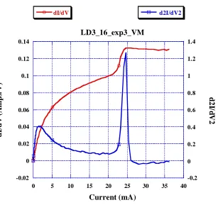
Figure 3.5 First derivative dV/dI versus current using current modulation. Laser threshold occurs at approximately 23 mA where dV/dI decreases abruptly. The kink at 0.01 amps corresponds to a range change. Above threshold, dV/dI is constant with a value~6.8 Ω (plateau)………...46
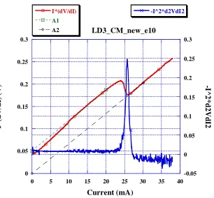
Figure 3.6 First derivative dI/dV versus current using voltage modulation indicating the laser threshold at approximately 23 mA. Above threshold dI/dV saturates at 0.133 siemens or (0.133)-1=7.52 Ω, which is the series resistance of the device……….………46
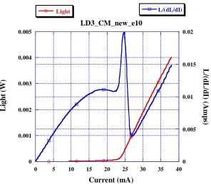
Figure 3.7 Light output versus current and dL/dI versus current in current modulation………...47
Figure 3.9 dV/dI and d2V/dI2 versus current. Threshold occurs when the second derivative first begins to decrease………...…49
Figure 3.10 dI/dV versus current and d2I/dV2 versus current in voltage modulation mode………...………..50
Figure 3.11 IdL/dV versus current in current modulation mode with two markers indicating the y-intercept of 0.05 below threshold and 0.002 above threshold. The slope Rs=6.8 Ω…..52
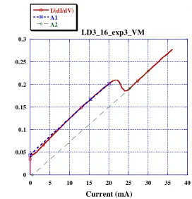
Figure 3.12 I/(dI/dV) versus current in voltage modulation mode, with a y-intercept of 0.044 below threshold and -0.0118 above threshold. The slope Rs = 8.02 Ω ………...53
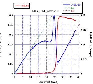
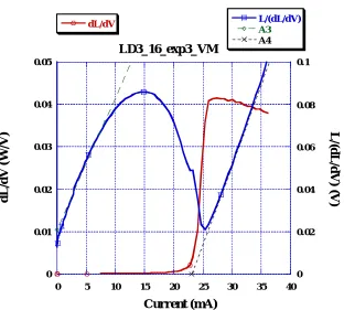
Figure 3.13 IdL/dV and -I2d2V/Ii2 plotted versus current in current modulation mode. Note that the baseline of -I2d2V/dI2 is nearly constant below and above threshold.……….54 Figure 3.14 dL/dI and L/(dL/dI) versus current. Slope of the asymptote before threshold is 0.844 and after threshold is1.008. X-intercept after threshold is 23.5 mA …………...…....56
Figure 3.15 Light output and L/(dL/dI) versus current……….………...57 Figure 3.16 dL/dI and L/(dL/dI) versus light output. The slope of the asymptote drawn is 3.67 and the laser diode has a wavelength of 650 nm or 1.907 eV, resulting in a quantum efficiency of 0.143. The asymptote cuts the y-axis on the right at 0.014…………...…...…..57
Figure 3.17 dL/dV and L/(dL/dV) versus current. Slope before threshold is 6.31 and after threshold is 7.54. The x-intercept of the asymptote drawn after threshold is 23 mA and the y-intercept of the asymptote before threshold is 0.116………..……….59
Figure 4.1 (a) Voltage versus current and light output versus current in current modulation mode. Threshold can be seen to occur at 2 mA. The differential quantum efficiency above threshold is approximately 0.26……….………..63
Figure 4.1 (b) Near field images of the oxide VCSEL showing threshold at 2 mA. The
intensity seems to increase gradually above threshold………64
Figure 4.2 First derivative (dV/dI) versus current in current modulation mode. The first derivative shows a sharp decrease at laser threshold of 2 mA ………..………...65
Figure 4.4 Light output versus current and dL/dI versus current in current modulation mode. The dL/dI has a sharp rise at threshold~2 mA. The nearly flat response of dL/dI beyond threshold indicates that the differential quantum efficiency is nearly constant………...67
Figure 4.5 IdL/dV versus current in current modulation mode. Y-intercept =0.072, η=2.77 and slope=24.25 before threshold and after threshold the y-intercept = 0.044, η=1.69 and slope=26.09………..69
Figure 4.6 IdL/dV and –I2d2V/dI2 versus current in current modulation mode. The sharp peak in –i2d2v/di2 indicates threshold. Two range changes appear as downward spikes at 0.8 mA and 4.2 mA ………...………...……70
Figure 4.7 First derivative of light (dL/dI) and L/(dL/dI) versus current in current modulation mode. The slope below threshold is 0.725 and that after threshold is 1.02. The x-intercept after threshold= 0.00195 which is the laser threshold………...…...71
Figure 4.8 First derivative of light (dL/dI) and L/(dL/dI) versus light output in current modulation mode. The emission wavelength of this laser is 850 nm or 1.459 eV. Note that at higher light levels the efficiency decreases slightly (deviates from the straight line) probably due to heating. The slope of the asymptote is 2.2………..….…….72
Figure 4.9 Near Field images of the oxide VCSEL………74
Figure 4.10 Voltage versus current and light output versus current in current modulation mode. Threshold can be seen to occur at 4 mA. The estimated upper limit of series resistance from the slope of the I-V curve is 27.8 Ω ………….…..………...………..…78
Figure 4.11 (a) First derivative (dV/dI) versus current in current modulation mode. The first derivative shows a sharp decrease at laser threshold. with respect to series resistance the most that can said is that it is less than 27 Ω ………...…………...……….80
Figure 4.11 (b) Near field images showing the appearance of the second smaller filament above the main filament pointed by the arrows at 4.8 mA, which grows in intensity upto 5 mA………81
Figure 4.11(c) Near field images showing the merging of the second filament with the main filament at 5.7 mA………...81
Figure 4.11 (d) Near field images showing the re-emergence of the second filament and the appearance of the third filament at 6.5 mA and the appearance of the fourth filament at 6.7 mA………82
Figure 4.13 dV/dI and d2VdI2 versus current in current modulation mode. Threshold is
indicated by a sharp decrease in the first derivative and a peak in the negative direction in the second derivative plot………..85
Figure 4.14 Light output versus current and dL/dI versus current in current modulation mode. The dL/dI has a sharp rise at threshold~2 mA ………..…..86
Figure 4.15 (a) First derivative dV/dI and dL/dI versus current. Note the high correlation of features between these two measurements………..87
Figure 4.15 (b) Near field images showing the brighter smaller filament “challenging the main filament at 4.2 mA, and the gradual rise in intensity of the smaller filament from 4.4 mA -4.6 mA……….88
Figure 4.16 IdL/dV versus current in current modulation mode………..90 Figure 4.17 IdL/dV and I2/d2V/dI2 versus current in current modulation mode..…………....91 Figure 4.18 Simple finite element model of the active region. A more complete model would have many volume elements in all three dimensions……….………...………...92
Figure 4.19 First derivative of light (dL/dI) and L/(dL/dI) versus current in current modulation mode……….…………95
Figure 4.20 First derivative of light (dL/dI) and L/(dL/dI) versus light output in current modulation mode. The slopes of the asymptotes are 3.59, 1.615 and 2.98………...…97
Figure 4.21 First derivative of light (dL/dI) and L/(dL/dI) versus light output in current modulation mode on an expanded scale. The slope of the asymptote below threshold is 7.219……….97
Figure 5.1 Plot of Junction voltage (V- IRs), versus I/Ith for the laser diode, oxide VCSEL and
LIST OF TABLES
Table 3.1 %Error in the calibrated first derivative measurements from the actual resistance values measured for different 1% resistors in current modulation and voltage modulation mode...40
1. CHAPTER 1- INTRODUCTION
1.1. Objectives
The main objectives of this work are to
Ø Construct, test and characterize a current modulation based derivative system for the
characterization of photonic devices.
Ø Compare the performance of the new current modulation system with an existing
system based on voltage modulation.
Ø Evaluate two types of Vertical Cavity Surface Emitting Lasers (VCSELs) with
varying degrees of optical confinement.
Ø Determine whether current modulation based derivative measurement can resolve
spatially dependent quasi Fermi level locking in multi-mode VCSELs above
threshold.
1.2. Motivation
Derivative measurements have been used to detect fine structure in the
current-voltage characteristics of semiconductor devices in general and these measurements were
done at NCSU using voltage modulation to help in better characterization of VCSELs. In the
region above threshold, i.e. at higher currents, a small voltage modulation results in a large
current sweep due to the exponential dependence of current which is expected to obscure
one’s ability to resolve fine structure. Hence, to be able to resolve fine structure at higher
In this chapter we discuss the history and development of the electrical and optical
derivative techniques and the successful application of these techniques in studying different
phenomenon in complex devices. A comparison is then made between the equipment used by
previous researchers to what we have developed along with a brief description of the
phenomenon of Quasi Fermi level locking. A brief history of VCSELs is presented that
describes the basic structure of a VCSEL and then the specifics of two different types of
VCSELs, the proton and the oxide VCSELs. Finally the chapter is concluded with the
advantages and applications of VCSELs.
The second chapter describes the experimental setup used for these measurements,
with emphasis on the various changes that were made to the existing voltage modulation
system, in order to be able to incorporate both current and voltage modulation measurements
to be taken with the same system. It also explains the experimental procedure employed to
test the devices. The third chapter includes a comparison of the voltage and current
modulation measurements illustrated using measurements taken on a stripe geometry laser
diode while explaining pros and cons of both the methods. Chapter four contains the current
modulation measurements taken on both the proton and the oxide VCSELs, their correlation
to the optical modes and lasing filaments, observations and their analysis. The last chapter
1.3. Electrical Derivatives: Prior Art
The technique of detecting fine structure in the current voltage characteristics of
tunnel junctions by measuring the derivatives dI/dV and d2I/dV2 has been widely used, and a number of systems were developed for making such measurements. This technique
commonly involves sinusoidally modulating an independent variable, such as current or
voltage, and detecting the ac response of the dependent variable, thus extracting the
derivative information using harmonic detection.1 The ac component of the device response
at the frequency of modulation provides a measure of the first derivative and that at the
second harmonic is proportional to the second derivative.1 These measurement techniques
were later used on transistors and double heterostructure semiconductor lasers.2
1.3.1. Derivative measurement techniques
The technique used to measure the first derivative dV/dI is similar to the well known
analog derivative techniques. The procedure relies upon superimposing an ac modulation,
ΔI=icos (wt) onto the dc bias current I applied to the laser. If the current modulation
amplitude i is kept small (relative to I) and constant, then the voltage V developed across the
device terminals may be written as a Taylor power series expansion in the modulation signal,
(
) ( )
( )
... 2 1 2 2 2 + ∆ + ∆ + = ∆ + = DC DC I I DC DC dI V d I dI dV I I V I I V V (1.1).... 2 ) ( cos ) cos( ) ( )). cos( ( 2 2 2 2 + + + = + = dI V d wt i dI dV wt i I V V wt i I V V DC DC (1.2) ... ... 1536 48 4 ) 2 cos( ... 192 8 ) cos( ... 4 ) ( 6 6 6 4 4 4 2 2 2 5 5 5 3 3 3 2 2 2 + + + + + + + + + + + = dI V d i dI V d i dI V d i wt dI V d i dI V d i dI dV i wt dI V d i I V DC (1.3)
Applying the above analysis to a simple diode current- voltage relationship given by
− −
= 0 exp 1
kT IR qV I
I s
η (1.4)
under the assumption I >>I0 near threshold, we get,
( )
(
)
... 1 2 1 1 2 ) 2 cos( 1 1 2 ) cos( 2 2 2 2 + − − − − + − − + = m m m q kT wt m m q kT iR wt I VV DC s
η
η
(1.5)
where, m = i/I is the modulation index, V is the externally applied voltage, Rs is the series
resistance of the device, η is the ideality factor, k is the Boltzmann’s constant, T is the absolute temperature and q is the electron charge.
By maintaining the modulation i much less than the bias current I (m<<1), only the
leading terms of each frequency component need to be retained and thus,
( )
cos(2 ) ...4 ) cos( 2 2 2 + + + = wt dI V d i wt dI dV i I V V DC
( )
cos(2 ) ...4 ) cos( 1 2 2 + − + + = wt I i q kT wt i I q kT R I
V DC s
η η
Thus, voltage detection at the fundamental frequency yields a direct indication of
dV/dI and thereby the values of Rs and ηkT/q can be extracted. Similarly, the signal at 2w can
be used to measure the second derivative d2V/dI2. Since Rs is a linear element and therefore appears only in the amplitude of the fundamental signal, the second derivative yields ηkT/q
directly.3 The second derivative in principle is proportional to the sinusoidal response at
twice the modulation frequency, but this method requires very high frequency selectivity in
order to reject the fundamental signal without appreciable loss of the second harmonic signal.
Also, the presence of even a small degree of harmonic distortion in the modulation signal
produces a second harmonic signal proportional to the first derivative as shown below:
We now consider the possibility that the ac modulation contains a second harmonic signal at
some undetermined phase θ, given by
( )
sin(2 )sin + 2 +θ
=
∆I Iw wt I w wt . (1.7)
With this modulation, the components of diode voltage at w and 2w are:
(
,)
sin( ) 2 cos( )2
2 +θ
+ = wt dI V d I I wt dI dV I w I V DC DC I w w I w
DC (1.8)
(
)
cos(2 )4 ) 2 sin( 2 , 2 2 2 2 wt dI V d I wt dI dV I w I V DC DC I w I w
DC = +θ − (1.9)
The second term in equation 1.8 is always negligible, and so we do not have any problem
detecting the first derivative. However, the first term in equation 1.9, is an unwanted signal,
minimize this interference. Our approach has been to use the difference frequency technique
as described below.
A dual frequency technique for electronically measuring high-order derivatives by
frequency mixing was developed by Paoli.1 In this method, an ac modulation at two distinct
but synchronous frequencies w1 and w2 is used to produce a derivative signal at a difference frequency w=w2-w1, which is unique to the order of the derivative being measured.1 With a small modulation i (t) superimposed on the bias current I, the series expansion for the voltage
V is
( )
n nn n
dI V d n
t i I
V t
V
∑
∞
=
+ =
1 !
) ( )
( (1.10)
In response to a current modulation applied at two frequencies w1 and w2, the linear term in
the expansion gives rise to sinusoidal components at w1 and w2, each of which is proportional to the first derivative dV/dI. Analogously, the quadratic term in the series produces signals at 2w1, 2w2 and w1-w2, all of which are proportional to the second derivative d2V/dI2. This
technique can also be applied to measurements of derivatives with orders higher than two.2
In our measurement circuitry, we used this dual frequency technique to measure the
first and second derivatives with respect to both current and voltage and also the first
derivative of light output with w1=15 KHz, w2=16 KHz and detecting the second derivative at the difference frequency, w = w1-w2=1 KHz. The advantages of using this technique are:
§ The frequency selectivity of conventional filters and lock in amplifiers can be used
§ The harmonic distortion of the modulation which produces a spurious signal
proportional to the first derivative does not contribute to the second derivative
measured at w1-w2.
Along with these electrical measurements a digital camera system captures the near field
images which will enable us to determine if there is any correlation of the electrical
derivative measurements with the near field mode structure. Optical derivative techniques
have also been described as powerful tools for investigating the electrical characteristics of
light emitting p-n junctions in complex devices, these measurements being independent of a
direct determination of the current-voltage relation, can be especially useful when analyzing
non ideal junctions.4
Nonlinearities in the emission characteristics of stripe geometry (AlGa)As double
heterojunction lasers have been studied to some extent with the help of derivative
measurements. The existence of nonlinearities in the current dependence of the output
intensity from (AlGa)As double heterojunction lasers has been noted by several authors6. It is
important to understand this behavior and its controlling factors and to determine the extent
to which these nonlinearities are a fundamental feature of junction laser behavior.6
Measurement of the first derivative dV/dI and the product IdV/dI is shown to be an
especially useful technique for electrical characterization, thereby allowing accurate
determination of lasing threshold, observation of voltage saturation and quasi Fermi level
pinning.3 Observation of the second derivative signal is useful because it provides a more
1.4. Quasi Fermi level locking
Diode lasers are non equilibrium semiconductor devices, and this is formally
described by the splitting of the Fermi level into quasi Fermi levels which describe the
distribution of electrons and holes individually. Under forward bias, the quasi Fermi levels
will split by the value of the applied voltage. Increasing the injection current in a diode laser
causes an increase in the number of injected electrons and holes into the active area. Below
threshold, this increase in current causes an increase of the carrier density within the active
region resulting in additional splitting of the Quasi-Fermi levels. At threshold, the gain is
equal to the loss. The losses in a simple laser diode are related to the mirror losses and a
small distributed loss co-efficient as shown below:
(
)
(
2)
1exp 2
1R Lγth −α =
R (1.11)
where, R1 and R2 are the mirror reflectivity’s, L is the cavity length, α is the distributed loss
co-efficient and
γth
is the gain at threshold. Solving forγth
we find + =
2 1
1 ln 2
1
R R L
th α
γ . (1.12)
At and above threshold, the gain is pinned at
γth
. Another way of saying this is that the roundtrip gain above threshold is equal to 1. The parameters R1, R2 and L are independent of the
optical intensity, and the loss co-efficient is very weakly dependent on the optical intensity.
Hence
γth
is essentially pinned at threshold. Since the gain is proportional to the excesscarrier concentration, the excess carrier concentration is pinned at threshold (the minority
tied to the excess carrier concentration the quasi Fermi level is pinned above threshold. In
general, the gain coefficient is given by
( )
ρ( ) ( )
ν ν πτ λ ν γ g r f 8 20 = (1.13)
where, ρ (ν) is the density of states, fg (ν) = Efc-Efv, is the quasi Fermi level separation.
The gain coefficient of a semiconductor laser amplifier has a peak value γp that is
approximately proportional to the injected carrier concentration, which in turn is proportional
to the injected current density J.
− ≈ 1 T p J J α γ (1.14) n qd J r i
T =ητ ∆ (1.15)
where, τr = radiative recombination lifetime, ηi ~ τ/τr = internal quantum efficiency,
τ = excess carrier lifetime, d = thickness of the active region, thermal equilibrium absorption coefficient, Δn = injected carrier concentration, JT = Current density required to just make the
semiconductor transparent.
The laser oscillation condition is that the gain exceed the loss, hence the threshold
injected current density Jth and current Ith, are given by
T r th J J α α α + = (1.16)
where, αr
(
αs +αm)
Γ = 1
αs , αm = loss coefficients due to mirror loss and other sources of loss, αr = resonator loss
coefficient, Γ = confinement factor, A= cross sectional area of the active region
From equation 1.15 it can be seen that, by increasing the injected current density J, the concentration of excess electrons and holes Δn is increased, and so is the separation between
the quasi Fermi levels. For sufficiently small J there is no gain. When J is such that Efc-Efv
just exceeds photon emission energy which is approximately the band gap energy, the
medium provides gain. The peak gain coefficient increases sharply and saturates at a peak
value. A further increase of J increases the gain spectral width but not its peak value (inhomogenous broadening).
Finally the junction voltage remains nearly constant above threshold since the quasi
Fermi level separation does not increase and remains locked at the value of the junction
voltage. An increase of the injection current only causes an increase in the optical power
without an increase in the junction voltage. We will see later that the locking of the quasi
Fermi levels essentially removes the diode characteristics from the circuit model and we can
extract the series resistance of the device. In summary, this is due to the requirement that the
gain=loss at threshold and results in the locking of the quasi Fermi level above threshold.
Using our derivative system, quasi Fermi level locking can be observed from the first
derivative measurements. Quasi Fermi levels are said to be locked when there is no or almost
1.5. Background on VCSELs
The VCSEL was first proposed and fabricated by K. Iga and his colleagues at the
Tokyo Institute of Technology, Japan in 1977. They successfully demonstrated the first
electrically pumped InGaAsP/InP VCSEL under pulse operation at 77 K in 1979.13 Later an
electrically pumped GaAs/AlGaAs VCSEL pulsing at room temperature was reported.14 In
1986, a GaAs VCSEL with threshold current of 6mA under continuous wave operation at
20.5 C was developed.15 Two years later, the first room temperature CW GaAs VCSEL
operating at 850nm was demonstrated. In 1989, Jewell demonstrated a GaInAs VCSEL
exhibiting a 1-2 mA threshold.
1.5.1. Structure of VCSEL
VCSELs are made by sandwiching a light emitting layer (i.e. a thin semiconductor of
high optical gain region such as quantum wells) between two highly reflective mirrors as
shown in Figure 1.1. The mirrors can be dielectric multilayers or epitaxially grown mirrors of
Figure 1.1 Model of VCSEL
1.5.2. Current and optical confinement structures
Along with the optical cavity formation, the scheme for injecting electrons and holes
effectively into a small volume of active region is necessary for the current injection device.
The threshold current depends on how small the active volume is and how well the optical
field can be confined within the cavity to maximize the overlap of the gain and the optical
field within the active region. Various confinement structures have been developed.
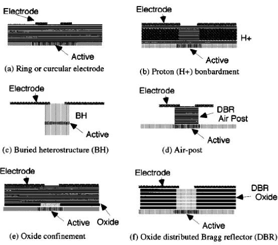
The current confinement can be achieved by
a. Ring or circular electrode type
b. Proton bombardment
c. Buried heterostructure type
d. Air post type
e. Selective AlAs oxidation type
These various current confinement structures are shown in Figure 1.2.
Figure 1.2 Structures for current confinement
Optical confinement schemes that have been developed so far include:
a. Fabry Perot type
b. Gain-guide type
c. Buried heterostructure type
d. Selective AlAs oxidation type
e. Antiguiding type
The purpose of these various optical confinement structures is to increase the overlap
of optical field with the gain region. Various implementations of optical confinement are
Figure 1.3 Structures for optical confinement
Devices formed from a λ/2 cavity, which consists of an InGaAs quantum well layer,
GaAs spacers, and an oxide aperture, sandwiched between the two mirrors have
demonstrated a threshold current of 91µA with an aperture diameter of 3µm.
The oxide aperture structure is obtained by oxidizing an AlxGa1-xAs layer so that a
layer of native oxide is formed. The native oxide layer has a relatively low refractive index
but high electrical resistivity.16 Hence, high performance can be achieved due to the precise
confinement of optical modes and injection current inside the active region. It has also been
shown that VCSELs with front and rear AlGaAs/GaAs DBRs can also form oxide apertures
inside the AlGaAs spacer layers to improve conversion efficiency.17
The rapid progress in the development of GaAs based VCSELs is due to the
promising properties of optical materials and the possibility of all monolithic structures,
including the epitaxial growth of DBRs. DBRs have been demonstrated successfully in
GaAs/AlGaAs Fabry perot micro cavities. The advantages of GaAs based DBR’s are that
they exhibit a wide variation in refractive index between adjacent layers so that fewer layers
are required to achieve high reflectivities18 and also low electrical resistance can be easily
obtained by using appropriate doping profiles.19 On the other hand, the use of optically
transparent contacts, such as indium-tin-oxide has improved the confinement of injection
carrier concentration inside the laser cavity.20
1.5.3. Advantages of VCSELs
The VCSEL provides a number of advantages compared to the traditional stripe
§ Ultra low threshold operation is obtained from its small cavity volume, reaching
microampere levels.
§ Emission wavelength is relatively insensitive to temperature variations.
§ Dynamic single mode operation is possible.
§ A large relaxation frequency provides high speed modulation capability. Research on
short-wavelength VCSELs has demonstrated modulation bandwidths as high as 16
GHz.21
§ Long device lifetime due to a completely embedded active region and passivated
surfaces.
§ High power conversion efficiency.
§ Vertical emission from substrate. The surface normal geometry enables the
construction of two-dimensional arrays of these devices.22
§ Easy coupling to optical fibers due to good mode matching from single mode through
thick multimode fibers.
§ A number of laser devices can be fabricated by fully monolithic processes yielding
very low cost chip production.21, 23
§ The initial probe test can be performed before separating devices into discrete chips
§ Easy bonding and mounting.
§ Cheap modules and package cost. The package configuration can be basically the
same as that of a detector and the low-divergence circular beam allows effective fiber
§ Vertical stack integration of multi thin film functional optical devices can be made
intact to the VCSEL resonator, taking the advantage of micromachining technology
and providing polarization independent characteristics.
§ Optical interconnections based on vertical-cavity surface-emitting lasers (VCSELs)
are expected to eliminate bottlenecks in electronic connections. They are also
expected to be used in constructing large-bandwidth switching networks and in
implementing, for example, massively parallel processors.23
They also find application in optical storage, print heads, optical sensors, barcode
scanners, displays, spatial light modulators, backplanes and smart pixels, and
microscopes.21, 22, 23
1.5.4. Proton bombarded and oxide confined VCSELs
The structures of the devices investigated in this work are shown in Figure 1.5. Both
the oxide confined and proton bombarded VCSELs have two sets of Bragg mirrors and a
cavity that will only support one Fabry-Perot mode. The main difference between the two
VCSELs studied is the confinement of the current and optical modes. The top side of the plan
view of the chip structure is shown in Figure 1.5. The optical output aperture is the small
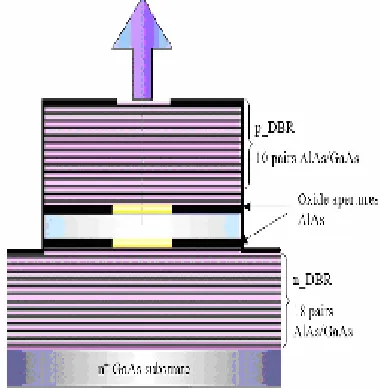
Figure 1.5 On the left is the proton VCSEL, where the smaller green dot surrounded by the blue ring is the output aperture. On the right the oxide VCSEL is shown, the output aperture is also the light green area inside the slotted orange circle.
Figure 1.6 a) Oxide confinement left, region 1 represents the multi-energy isolation implant for insulating purposes, region 2 in the figure contains the PN junction (quantum well region), region 4 is the annular ring of aluminum oxide represented by the dark gray stripe, region 5 represents the removal of acceptor concentration in that area; b) Proton implantation right, region 1 represents the multi-energy isolation implant for insulating purposes, region 3 shown by the dark gray area is the gain-guided proton implant, region 2 in the figure contains the PN junction (quantum well region). Figure from Honeywell.
Current confinement is necessary to obtain low Jth at room temperature along with
other benefits. Restricting the current using the proton implantation scheme creates a region
of high resistance that restricts the flow of current to an opening in the implanted region. The
(region 3) in 1.6(b). The high lateral sheet resistance below the gain guide gives excellent
debiasing of the P-N junction at the isolation implant perimeter. A problem encountered with
ion implantation is the damage that occurs when the implantation is done. If the active
region is damaged, defects such as recombination centers may be found creating a significant
ηkT current under the gain guided implant area.
Since the pioneering work on wet oxidation of aluminum containing III-V materials
by Holonyak and co workers, the application of selective oxidation has greatly enhanced the
performance of VCSELs by providing improved electrical and optical confinement. Oxide
confined current works more like a dam for water constricting the current flow to a small
region through an opening in the dielectric (region 4). The wet thermal oxidation process
forms an annular ring of aluminum oxide represented by the dark gray layer (region 4) in
Figure 1.6(a). The oxidation process also removes acceptor concentration from the
equivalent of six mirror periods plus the oxide thickness as illustrated by the dotted region
(region 5) around the oxide layer in Figure 1.6(a). In this case, the sheet resistance of the
P-type layer under the oxide is a function of the thickness and placement of the oxide layer
relative to the quantum wells. While both methods confine the current, the oxide method
also helps to confine the optical mode to the active region due the abrupt dielectric interface.
Selective oxidation is an efficient and convenient current confinement scheme which,
because of superior electrical confinement within the active area, leads to record low
thresholds and high wall plug efficiency compared to other VCSELs. The optical modes too
are more tightly confined in the active area than for an implanted VCSEL, resulting in low
1.5.5. VCSELs and derivative measurements
Proton implantation has been widely used in fabricating VCSELs since it provides
good lateral electrical confinement resulting in relatively low-threshold devices. It is also an
attractive method for isolating individual VCSELs on a wafer yielding planar structures with
small geometries.24 Electrical derivative measurements were used to obtain an improved
understanding of the various current paths and also measure the variation of bulk series
resistance in proton implanted VCSELs.24
Electrical derivative analysis has been employed to obtain prominent features in these
devices by correlating the electrical derivative IdV/dI curve with the polarization resolved
optical output power (L-I curves) and the optical spectra.25 This derivative characterization provides an efficient and precise method to determine the onset current of the higher-order
mode lasing. The electrical derivative analysis is a useful tool to determine the major
operating currents of selectively oxidized VCSELs. The electrical and optical characteristics
2. CHAPTER 2 - EXPERIMENTAL SETUP
2.1. Introduction
This chapter lists the measurement devices used and the manner in which they were
setup in order to obtain electrical and optical derivative measurements on the various
photonic devices. Most of the equipment used in this setup was custom built. The equipment
used consists of a derivative machine, a photodiode test fixture, a camera test fixture,
Keithley multimeter, EG&G lockin amplifier, an oscilloscope and a computer. The manner in
which the equipment listed above has been setup to achieve the desired task is shown as a
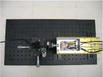
block diagram in Figure 2.1. A photograph of the entire experiment setup is shown in Figure
2.2. The primary piece of equipment is the derivative machine. It is a multi functional tool
capable of performing various measurement tasks. The computer runs a custom written
HTBasic program and interacts with the derivative machine for automated data acquisition.
The test fixture holds the device under test in an isolated environment to capture the
electrical and optical response from the device. The Keithley multimeter acts as an analog to
digital converter and the EG&G lockin was used instead of the custom built lock in amplifier
present in the derivative machine for comparison purpose. The oscilloscope served to
observe the waveforms at intermediate stages of the experiment run in order to affirm if the
setup is working as expected and if not it helps to isolate any problems. The derivative
machine, the Keithley multimeter and the EG&G lockin amplifier were connected to each
Figure 2.1 Block diagram of Experimental Setup
Figure 2.2 Experimental setup consisting of the derivative machine, a voltage test fixture lying on top of the derivative machine. To the right of the derivative machine is the camera test setup and to the left is the Keithley multimeter on top of the EG&G lockin amplifier. On the other side of the Keithley multimeter lies the computer and an oscilloscope can be seen on the extreme left of the picture.
Derivative Machine Keithley
EG&G Lockin
Computer
Test Fixture
GPIB
GPIB GPIB
DUT High
DUT Low Vdc Vac
gnd
2.2. Derivative Machine
The derivative machine consists of a power supply and twelve slots for custom built
rack mountable cards to interface with a computer via an IEEE 488 GPIB. This machine was
built and the circuitry completed by Dr. Robert Kolbas. This apparatus uses analog
modulation and phase sensitive signal recovery of the signals associated with the first and
second derivatives. It is capable of performing both Voltage modulation and Current
Modulation. The computer controls the mode in which the derivative machine is to operate
switches the equipment setup accordingly. There are two LED’s indicating whether the
current setup is for the current modulation or the voltage modulation. It also has LED’s
which light up in the event of current overload. A block diagram of the derivative apparatus
is shown in Figure 2.3 along with a photograph in Figure 2.4.
The interface cards currently present are:
§ Waveform generator
§ Digital to Analog converter
§ Two current to voltage converters
o One for electrical feedback from the device under test
o One for the optical feedback from the photodiode
§ Switch box for routing signals
§ Lock-in amplifier
Figure 2.3 Block diagram of derivative machine.
Figure 2.4 Derivative machine wired for the experiment showing the different interface cards.
Waveform Generator
I/V Converter Electrical
I/V Converter Optical
D/A Converter
Switch
Lock – in Amplifier
A/D Converter
From Computer
Vac DUT low
Photo diode
DC out
DUT High
To HP out
BP out
DC out
AC out
Ref
Test 1
Test 2
To Keithley
The functions of these plug-in boards and their interaction with the each other and the
computer are as follows:
Waveform generator
The computer downloads the appropriate waveform , i.e. 1 KHz wave for the first
derivative and (15KHz + 16KHz) for the second derivative, into this module which supplies
ac modulation and also a 1 KHz TTL wave which serves as a reference waveform for the
Lock-in amplifier and also the oscilloscope in order to trigger the oscilloscope with the
external reference signal.
Digital to Analog Converter
This module generates a dc signal proportional to the digital data received from the
computer. The dc signal is subsequently combined with the small ac signal from the
waveform generator and the combined signal is output as either a voltage or a current.
I to V converters
These are two low impedance current to voltage converters employ transimpedance
amplifiers to convert a current to a voltage with (Vout = -RfIin) where Rf ranges from 107 or
106 to 10 ohms in decade steps for the light and current signals respectively. These modules
also perform filtering functions to separate the ac and dc signals. The block diagram of the
I-V converter is shown in Figure 2.5, the two inputs DUT low and I-Vac fed from the test fixture
are routed appropriately to allow for both voltage modulation and current modulation
measurements. When in current modulation mode, the two switches connect to the nodes
labeled ‘NO’ and in voltage modulation mode they connect to the nodes labeled ‘NC’. Then,
(high pass output) and ac voltage for the second derivative (band pass output) respectively.
The dc signal is sent to an ADC and the ac signals are fed to the lock in amplifier via the
computer controlled switch module. The difference between the two I-V converters is that,
the I-V converter used for the electrical feedback has two inputs coming from the test fixture,
one of which (DUT low) carries the signal required for voltage modulation and the other is
for the current modulation. Depending on the measurement being made one of the inputs is
fed to the transimpedance amplifier within the module.
Figure 2.5 Block diagram of I/V Converter. DUT=Device under test. Switch down (NC) is voltage modulation mode. Switch up (NO) is for current modulation mode.
Lock-in amplifier
This module receives the inputs from the I-V converter and recovers the ac signals for
the first and the second derivatives using phase sensitive detection relative to a 1 KHz
reference signal. The output of the recovered first derivative signal is fed to an ADC and the
output of the second derivative signal is sent to the Keithley multimeter. This module also _
+
HP
BP LP
DC out
HP out
BP out DUT low
Vac
Rf
NC
NC NO
NO Chassis
Ground
Special Ground
has two test ports on it which allow the user to view the first and the second derivative
waveforms on an oscilloscope to check if the phase sensitive detection is being done well.
Analog to Digital converter
This module consists of a four channel (15bits + sign) analog to digital converter.
Each channel has dual ranges ± 15V and ±0.3V.
2.3. Keithley Multimeter
This 5
2
1 digit multimeter acts as an analog to digital converter and is used in this
setup for the digitization of the second derivative output in order to get a better precision over
the custom built ADC present in the derivative machine. The option to integrate the signal
over several power line cycles (PLC’s) is used to reduce the noise in the second derivative
signal.
2.4. EG&G lockin amplifier
This lock in amplifier was used in place of the existing built in lockin amplifier with
the hope to obtain better phase sensitive recovery and have higher noise immunity compared
to the custom built lock in amplifier.
2.5. Test fixtures
To hold the device under test and capture both the electrical and optical output from
it, two test fixtures were built, one of which is the voltage- photodiode test fixture and the
other is the voltage-camera test fixture. Both test fixtures use coax cables to connect to the
Inside the two test fixtures is a proto board, to provide electrical and mechanical support to
the device under test. Some simple circuitry was built to allow for both voltage and current
modulation measurements to be taken with the same holder. The Block diagram in Figure 2.6
shows the circuitry and the connections for this board.
Figure 2.6 Circuit diagram of the instrumentation amplifier built into the test fixture. Laser diode (not shown) is connected between DUT high and DUT low.
The DUT high input coming from the DAC of the derivative machine is given to the device
under test which is connected to an instrumentation amplifier, the output of which is
available on the Vhigh pin. This output is passed through a high pass filter to obtain the ac
signal, which serves as an input to the I-V converter in case of current modulation. The other +
_
2
3
4 5 7
6 DUT
High
DUT Low
VHigh
dc out GND +15 -15
VLow
end of the device under test is connected to DUT low for voltage modulation measurement
that serves as the input to the I-V converter and is connected to ground for current
modulation measurements. The simplified circuit that would result for voltage and current
modulation measurements can be seen in Figure 2.7 and Figure 2.8 respectively.
Figure 2.7 Voltage modulation-Test fixture.
Figure 2.8 Current modulation- Test fixture.
2.5.1. Voltage-Photodiode test fixture setup
The voltage test fixture setup includes two die cast aluminum boxes of differing sizes
that contain the laser diode and mounting apparatus that hold the laser diode. The smaller +
_
Instrumentation Amplifier
DUT
DUT High
DUT Low Vdc
+
_
Instrumentation Amplifier
DUT
DUT High
Vdc
and 5.5cm deep. The larger box has four leg posts with rubber soles for insulating purposes.
The smaller box also has four leg posts that are used to elevate the small box. Inside the
smaller box a hole was cut into the shorter wall for a connector for a photodiode to be
screwed in place. Different photo diodes can be placed inside the box for testing of different
wavelengths or low light output. The smaller box is covered with the larger box for extra
light containment and to keep ambient light away from the photodiode. The wiring for the
photodiode runs through holes in the larger box.
Figure 2.9 Full view of the Voltage Photodiode test fixture without the inner cover and external light shield removed.
Inside the smaller box is a proto board described earlier with connection pins sticking
upwards. This holder for the laser diode slides onto the connector pins and holds the laser
diode as seen in Figure 2.9. The photodiode receives light output from the laser diode and
the current output from the photodiode is passed via coaxial cables to a second I-V converter
to separate the Vac and Vdc can not be used for the second derivative and optical
measurements because this particular I-V converter does not have a band pass filter to isolate
the low level difference frequencies.
2.5.2. Voltage – Camera test fixture setup
To determine if electrical and optical measurements can be correlated and used to
characterize the laser, a camera setup was constructed allowing for the near field optical
mode patterns to be photographed. With the capability of photographing the optical mode
patterns, the correlation between modes and voltage/current measurements may be observed.
Another advantage of having the mode patterns visually is that any shifting in the modes
could be paired with the nonlinearities found in the data being retrieved.
The camera box setup consists of a die cast aluminum box holding the device under test
similar to the voltage box setup as shown in Figure 2.10, except that it does not have the
photo diode attached to it. Instead a 1 inch diameter hole was cut into the side wall facing the
device under test to allow for the light output from the device under test to be captured by a
microscope objective attached to the camera for the near field images. This smaller box has
four leg posts and is affixed to an aluminum platform 10 inches long and 3.8 inches wide.
The aluminum platform has four leg posts and is attached to the optical bench. The top view
of the camera test setup can be seen in Figure 2.11. We did not use two aluminum boxes for
the camera setup as we did for the photodiode setup because so much of light containment
wasn’t necessary in this setup. Inside the smaller box is the proto board to which the device
to the one used in the voltage- photodiode test fixture except that there is no photo diode
output cable.
Figure 2.10Voltage camera test setup showing the test fixture and the camera fitted with a microscope objective lens of 100X magnification.
Three stages, which serve as a XYZ translation device, hold the camera and
microscope objective. The X and Y directions can be seen in Figure 2.11 and the Z direction
is coming out of the page. The side view of the experiment setup seen in Figure 2.12 shows
the Z direction and the manner in which the test fixture is mounted on the optical board.
Mounted on the front of the Z direction stage is the camera and objective lens holder. Epoxy
was applied to a plastic mount for the camera and placed directly on a piece of metal with a
threaded hole for the objective lens. The camera screws into the plastic piece on one side and
the objective lens is screwed into the other. The camera is hooked to a computer via USB
The purpose of this setup is to obtain electrical derivative measurements while
observing the optical mode patterns and any irregularities that may be present. Using the
microscope objective to image the optical pattern on the chip allows for a closer look at the
near field. High power microscope objectives require a close working distance. Devices that
are packaged with a protective cover (can) limit the magnification to about 20 X due to the
space between the device and the protective window. We have operated the system with
objectives up to 100X on devices with the chip exposed by removing the can. Below is the
image of a proton VCSEL at 20X and 40X. The 100X objectives have proved to be
troublesome when trying to take images. The small working distance of the 100X objective is
only a few micrometers.
2.6. Programming issues
The computer programming language used on the PC is called the Trans Era HT
Basic. This program was modified to allow for current modulation measurements to be taken
along with the voltage modulation measurements, and also to choose to use either the built in
lockin amplifier or the EG&G lockin amplifier.
Once the program is running, a user is prompted to answer a number of questions.
The first few questions are used to setup the derivative machine and set all interface cards
used for input and output to zero. The next set of questions deals with the test devices and
what type of measurement is to be taken, the choices being, voltage modulation with either
the old test fixture or new test fixture, or Current modulation with the new test fixture.
Limiting input values are also set at this point so the device is not over driven. Once all the
recording the responses from the diodes. First the program takes an I-V and light output
measurement, which sets boundaries for gain values for voltage inputs. Next the program
runs through the first and then the second derivative measurements. The last measurement
taken is the light derivative measurement. When taking the second derivative, the
measurement can be integrated over one or ten power line cycles (PLCs). Electrical power
lines have a 60Hz frequency that the program uses to calculate the integration time of the
derivative measurements. Graphs and data are displayed on the computer screen to keep
track of the current input value. Once the program has run its course, a few options become
available to the user. Initial plots of the data just taken can be printed for evaluation of any
visible undesirable data. Another option is for the data to be stored in a given file folder.
The other options pertain to repeating the measurement or starting a different measurement.
After the data is acquired and stored in text files in a folder the graphing program
kaleidagraph is used to plot the data. A short automated program was written with
kaleidagraph to plot the data in a given format. The data can be plotted in pairs for
comparison, for example the first and second derivative can be plotted on top of one another
in different colors. Overlaying the plots help identify many of the irregularities found in the
derivatives. Plotting the data in pairs is also helpful with respect to correlating the optical
and electrical derivatives.
Labview is used to control the camera when taking the images of the optical modes
while running the program. In order to take a picture of the optical mode at every voltage or
current step both the HT Basic and Labview programs had to be interfaced in some manner.
accesses and writes a one or zero corresponding to different commands for the camera. HT
Basic also writes information to another file corresponding to what measurement is being
taken at that given point. This information is used for the name of the file to keep track of
3. CHAPTER 3-COMPARISON OF CURRENT MODULATION AND
VOLTAGE MODULATION MEASUREMENTS
This chapter describes how the derivative machine is prepared to take the
measurements and how the voltage modulation and current modulation measurements are
taken. We then, compare the voltage modulation and current modulation quantitatively and
the measurements obtained from the derivative machine with the appropriate plots. The
voltage and current modulation comparison was done using a standard stripe geometry edge
emitting laser diode.
3.1. Derivative system
The derivative system, along with the two measurement test fixtures described in
Chapter 2, allow for the electrical and optical derivative measurements to be taken on any
device, be it a simple diode or a complex device like a VCSEL. The computer controls the
derivative machine and stores the observational and numerical data, and the plotting program
Kaleidagraph is used to plot different graphs for the purpose of analyzing and interpreting the
data. The voltage test fixture provides the I-V measurements, electrical derivative measurements and the optical derivative measurements whereas the camera test fixture
provides only the I-V measurements and the electrical derivative measurements and captures the near field images. The derivative system has been calibrated to account for the phase
changes, and also to be able to record calibrated data for the light measurements, first and
second derivatives.
3.1.1. System Calibration and test