ISSN 2348 – 7968
713
Purpose of Low-Power Linear Feedback Shift Register (LFSR) by
using Bipartite and Random Injection Method for Low Power BIST
1
D.Haribabu, 2J.RaviKumar, 3C.Ramesh Reddy
1&2Asst. Prof. Siddartha Institute of Science and Tech, Dept.of ECE, Puttur, Chittoor (Dt), A.P.
3Asst. Prof. Sri Venkatesa Perumal College of Engineering & Technology, Dept. of ECE, Puttur, Chittoor (Dt), A.P.
Abstract
In a bit of electronic systems that was practiced in safety critical application circuit testing has to be done periodically. For these systems, power dissipation due to BIST [built in self-test] represents a substantial portion of overall power dissipation. The power dissipation during the test mode is 200% more than in a normal manner. This report recommends a low power Linear Feedback Shift Register (LFSR) for Test Pattern Generation (TPG) technique of sinking power debauchery during testing. The correlations between the sequential patterns are higher during normal mode than during testing. The proposed approach utilizes the concept of bringing down the transitions in the test pattern generated by conventional LFSR [3] thereby reducing the force.
Keywords: LFSR, Optimization, Low Power, Test Pattern Generation, BIST
1 Introduction
Nowadays, many courses include on-chip structures that facilitate self-testing known BIST. The power debauchery during the test mode 200% more than in normal manner. Hence, it is a significant aspect to optimize the power during testing. In that respect are main two sources of power dissipation in digital circuits; these are static and dynamic power dissipation. Static power dissipation is mainly due to leaking current, and its donation to the total power dissipation is minuscule. Dynamic power dissipation is due to switching [1], i.e. the power used up due to short circuit current flow and charging of load capacitances is given by the equation:
P0.5
V
dd2E SW C f( ) L CLk (1)ISSN 2348 – 7968
Nevertheless, power reduction using the switching action does not degrade the operation of the tour. Since the power dissipation in CMOS circuits is directly proportional to the switching activity, hence, the excessive switching activity may be responsible for the monetary value, dependability, operation verification and technology related problems. For testing complex circuits, a hierarchical approach is applied. The vantage of the hierarchal approach is that, every block was tested on an individual basis. That is the test input given for each cube, and yield of each blockage is noted and verified. DFT (design for testability) [2] is a technique practiced in the chip design process to enhance the power to generate the test vectors, to achieve the measured quality level and to bring down the price of testing. We practice the conventional DFT approaches such as scan and BIST. In this paper, a modified LFSR [3] is proposed which reduces the number of passages in the test forms.
2 Prior Work
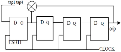
Linear Feedback Shift Register is a route consisting of flip-flops associated in series with each other. The output of one flip-flop is connected to the input of the next flip-flop and so on. The feedback polynomial that was likewise known as the characteristic polynomial is used to find the feedback taps which in turn defines the duration of the random pattern generation. An example below in Fig 2 is used to demonstrate a correlation between the LFSR, its characteristic polynomial and matrix theory. In the circumference, the feedback taps are shown to be from the output of the 4th and first register.
Fig 2 Conventional LFSR
ISSN 2348 – 7968
715
[2] that during normal operation of well designed CMOS circuits the switching activity power accounts for over 90% of total power dissipation.
Therefore, power optimization techniques at different layers of abstraction target minimal switching operation control. In Eq (1), the power dissipation can be shortened if we cut down the supply voltage or clock frequency. Only this will degrade the operation of the organization. C is the function of process technology and therefore not under the command of the architect. Thus, the power dissipation is directly proportional to the switching action. The grounds for increased power in test mode are:
1) To test the large circles, they are partitioned to make unnecessary the test time, but the parallel testing results in excessive energy and power waste.
2) Due to lack of at speed equipment availability, the time lag is introduced in the circuit during testing. This postponement will cause the power dissipation[4].
3) Due to lack of correlation between the successive patterns, there survives a massive represented as BT, BT2, BT3, where B is the seed vector. The determinant of the T matrix is called the characteristic polynomial, and the generator polynomial is the opposite of the characteristic polynomial. The increased power consumption of the device in the developed test environment. Therefore, can in most cases surpass the maximum power utilization specification of the IC resulting in un-repairable device failures begin with a pattern engender using a conventional LFSR causing important loss of return.
Earlier Techniques for scaling down the power dissipation during testing are:
RSIC (random single input change) test generation, which is applied to get a low power test pattern. In this method, energy consumption is reduced, merely at the additional price is between 19% and 13%. Another technique is proposed in [3] that is Low transition LFSR for BIST applications. This technique
cuts down the average and peak power of circuit during testing.
In [4], a Fault model& ATPG algorithm is taken first, and then test patterns are generated to achieve the desired fault coverage.
F.corno et al. Offered a Low power test pattern generation for the sequential circuit in [5]. In this paper,
redundancy is brought out during testing. This technique will cut the power consumption without affecting the fault coverage.
ISSN 2348 – 7968
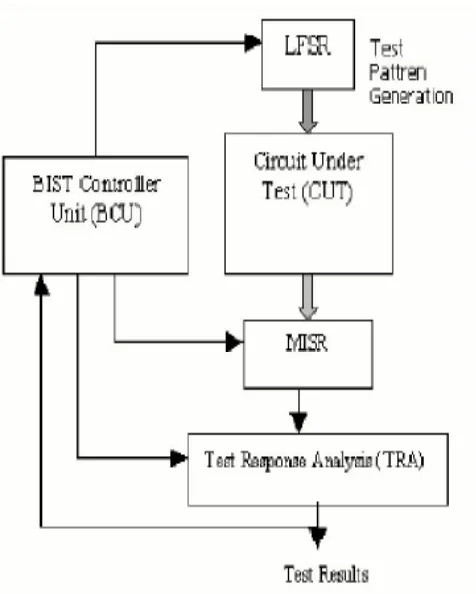
It is imperative to take the proper LFSR [3] architecture consumes different power even for the same polynomial. Another Problem associated with choosing LFSR is the LFSR design issue, which includes LFSR partitioning, in this the LFSR are differentiated on the basis of hardware cost and testing time cost. A typical BIST architecture consists of a test pattern generator (TPG). Usually carried out as a linear feedback shift register (LFSR), a test response analyzer (TRA), implemented as a multiple input shift register (MISR), and a BIST control unit (BCU).
Fig 3 BIST Architecture
The components of BIST architecture was given below.
1. Test pattern generator (TPG): it generates test patterns for CUT. It is an LFSR or ATPG.
2. The circuit under test (CUT): it is the circuit to be quizzed. It can be either combinational, sequential or memory.
3. Multiple input signature register (MISR): it was considered for signature analysis, which is a technique for data compression.
4. Test response analysis (TRA): it evaluates the value of primary output with the expected output.
ISSN 2348 – 7968
717
In this report, a low power LFSR is proposed for BIST applications
The purpose of Advanced LFSR:
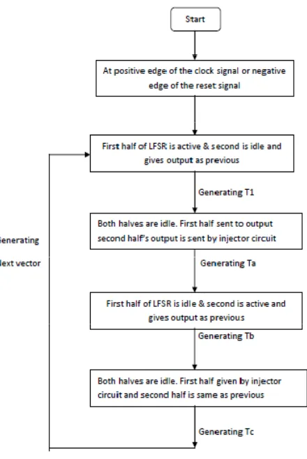
We suggest a random shape generator that mix two methods of test pattern generation called R-Injection (RI) and Bipartite LFSR. Briefly, the RI method introduce a new intermediate pattern between two consecutive test patterns. By placing a random bit (R) in the corresponding bit of the intermediate pattern when there is a transition between equivalent bits of pattern pairs. The Bipartite LFSR produces an intermediate pattern using one-half of each of the two consecutive random patterns.
The primary advantage of our proposed technique is that it can exist for both combinational and sequential circuits, and the randomness quality of the models does not degenerate. Thither are many suggested methods of random pattern generators that only reduce the transitions either within the shapes or between the patterns by an n-bit LFSR. The maximum number of changes will be n when Ti and Ti+1 are the complements of each other. One strategy used to shorten the number of changes to a maximum of n/2 is to insert a pattern the half of which is identical to Ti and Ti+1. The Bipartite strategy guarantees the development change to incomplete ton/2 between two consecutive practices. To preserve the randomness of patterns, instead of the Bipartite strategy, we randomly inject a value in bit positions where the ≠ tji+1, We insert a random bit R if the corresponding bits in Ti and Ti+1 are different. Notice that since such men are uniformly administered and also we replace them with another random value the overall randomness remains unchanged, i.e. H =n. Unluckily, the maximum bit transition can be no longer undertaken, although the anticipated number of transitions (mean value in the normal distribution) will be n/ 2.
Algorithm for Low Power LFSR:
ISSN 2348 – 7968
between these five vectors is equal to the number of signal transitions between T1 and T2. Fig 3.1 shows proposed an algorithm for Low Power LFSR.
Hence, the power consumption is cut. Additional circuitry is involved to generate three intermediate vectors. The EDA tool was utilized in which conventional, and low power LFSR was coded in Verilog hardware description language Xilinx 10.1. The outputs of 36-bit LFSR were used as inputs to C432 ICSAS-85, a benchmark interrupt controller. In this c432 is used as CUT.
Fig 3.1 Proposed Algorithms for LPLFSR
4 Conclusions
It was noted that the total power consumed in modified LFSR was 46% less than the regular LFSR. Moreover, dynamic power is lessened by 44.6% [7]. It was closed that low power LFSR is very a lot useful for power optimization of BIST. The solutions obtained from Xilinx 10.1 will be implemented on xc3s200-4pq208. VCD file was generated after post-simulation. X power is employed to estimate the energy use. Take the seed value to the 36-bit LFSR is (01001010010110101101001O100101101011).
ISSN 2348 – 7968
719
Table 4.1Comparison of X or LFSR – LP LFSR
Future Work:
Power dissipation in BIST can also be tested pattern reordering with the aim of cutting down the quantity of energy dissipated during circuit testing. By reordering test patterns, one can get the test. Sequences for which power dissipation minimized.
References
[1] F. Najm, “Transition Density, A New Measure of Activity in Digital Circuits”, in IEEE Transaction on Computer-Aided Design no.2, vol.12, pp.310-323, February 1993.
[2] A. Chandrasekaran, T. Sheng and R.Brodersen, “Low-Power CMOS Digital Design”, in IEEE Journal of Solid-State Circuits,
[3]. Mohammad Tehranipoor, Mehrdad Nourani, Nisar Ahmed, “Low Transition LFSR for BIST Based Applications [4]. Fulvio Corno, Paolo Pinetum, Matteo Sonza Ford “Testability Analysis and ATPG on Behavioral RT- Level VHDL”,
[5]. F.Corno, M.Rebaudengo, M.Sonza Reorda, “A Test Pattern Generation Methodology for Low Power Consumption”, pp.1-5, 2008.
[6]. Dr. K. Gunavathi, Mr. K. Paramasiva, Ms.P. Subashini Lavanya, M.Umamageswaram, “A Novel BIST TPG for Testing of VLSI Circuits”,
[7]. Balwinder Singh, Arun Khosla, Sukhleen Bindra, “ Power optimization of LFSR for Low Power BIST”, IEEE
International Conference 2009, pp. 311-314.
AUTHORS PROFILES;
ISSN 2348 – 7968
2]. Asst. Prof J. Ravikumar did his B. Tech insiders Institute of Engineering & Technology and M. Tech from Siddarth Institute of Engineering & Technology, Puttur, my Interest Areas are Embedded System Design.I publish a 1 Inter National Level Publications (Journals).I attended 2 International Workshops. I have 2years experience of Teaching in various colleges. Presently working in the Siddartha Institute of Science and Technology, Puttur. As an Asst. Professor in the Dept. Of ECE.,