Simulation of a Fast Timing Micro-Pattern Gaseous
Detec-tor for TOF-PET and future acceleraDetec-tors
RaffaellaRadogna1,2,∗,PietVerwilligen1,2, andMarcelloMaggi1,2
1INFN, Bari, Italy
2University of Bari, Bari, Italy
Abstract. Simulation is a powerful tool for designing new detectors and guide the construction of new prototypes. Advances in photolithography and micro-electronics led to the development of a new family of devices named Micro-Pattern Gas Detectors (MPGDs) [1], with main features: flexible
geom-etry; high rate capability (>MHz/cm2); excellent spatial resolution (<100µm);
good time resolution (5-10 ns); and reduced radiation length. A new detector layout, named Fast Timing MPGD (FTM), has been recently proposed [2] that would combine both the high spatial resolution and high rate capability of the MPGDs, while improving the time resolution with nearly two orders of
magni-tude to∼100 ps. However charged particle timing with gaseous detector time
resolution below 100 ps has been established with another detection scheme [3], this approach might not be able to sustain high particle rates. This contribution investigates the use of the FTM technology for an innovative TOF-PET imaging detector and emphases the importance of full detector simulation to guide the design of the detector geometry and performance.
1 Fast timing micro-pattern gas detector
Recently, a multi-layered detector with alternating drift and gain regions and resistive elec-trodes has been proposed [2]. In the drift region primary electron-ion pairs are created along the path of a charged particle passing through the detector, and they drift (due to a moderate electric field) to the gain region, where these primary electrons are multiplied and a detectable electric signal is created. The signals from each multiplication stage are read by the external readout electrodes through capacitive coupling. The time resolution of those Fast Timing MPGD (FTM) is governed by fluctuations in the distance between the closest electron-ion pair and the gain region and is improved reducing the drift distance of the closest primary electron by having several drift regions competing with each other, where the fastest drift time determines the time resolution.
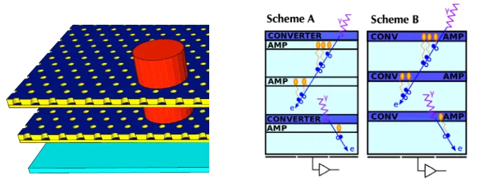
Figure 1 (left) illustrates a 2-layer structure of the FTM. Not shown is the top cathode
plane made of a polyimide foil covered with ∼100 nm of Diamond Like Carbon (DLC).
The coverlay spacers (red) of 250µm height separate anode and cathode and define the drift
gap. The amplification structure then consists of a polyimide foil of 50µm height, covered
also with DLC. Thjis foil is mounted on top of a polyimide layer with both top and bottom covered with DLC. The top DLC electrode is connected to ground and serves to induce a high
Figure 1. Illustration of a 2-layer FTM (with missing top electrode, left) and two possible detector schemes for the detection of 511 keV photons (right).
electric field inside the hole, while the bottom DLC coating serves as the cathode electrode for the next FTM layer. With top holes of 50µm and bottom holes of 70µm diameter spaced 140µm apart, which are the standard diameters and hole-spacing for GEM technology, a gain of∼5000 should be reachable in Ar:CO2(70:30) putting the anode at 500 V (100 kV/cm
amplification field) and cathode at 575 V (3 kV/cm drift field).
2 Fast timing micro-pattern gas detectors for TOF-PET
Positron Emission Tomography (PET) is an imaging technique used to visualize organ and tis-sue functions. A positron-emitting radio nuclide (tracer) inside a biologically active molecule concentrates in tissues with high metabolic activity. The tracer undergoesβ+decay, produc-ing a positron that will annihilate (whithin∼1mmfrom the emission point) with an electron. Thise+e−annihilation produces two back-to-back photons with energy of 511 keV. The detec-tion of two coincident 511 keV photons allows to reconstruct a straight line (line of response, LOR), along which the annihilation took place. The measurement of several hundreds of thousands of LORs allows to reconstruct the concentration of the tracer.
In Positron Emission Tomography (PET) the quality of the reconstructed images can be improved when time-of-flight (TOF) information is used by reducing the zone of the positron emission to a fraction of the length of the Line of Response, leading to a higher contrast image and more accurate diagnoses [4]. The fine time resolution also allows to constrain the coincidence window for the two photons to be detected, leading to lower background.
Modified FTM detector layers specialized for TOF-PET are under study to optimize their ability to detect of 511 keV photons from positron annihilation. Two preliminary detector schemes are presented in Figure 1 (right): Scheme A where the photon converts in a dedicated layer and there is competition in two or more active area layers in order to optimize the time resolution; Scheme B where the amplification layer is made of material with high photon conversion efficiency in order to optimize the detection efficiency. Both schemes rely on the Compton scattering process to liberate an electron in a converter material with enough kinetic energy to reach the sensitive gaseous volume of the detector. For this reason, no energy measurement can be made. Using ADC counts or cluster counting low enenergy background electrons can be discriminated from hard Compton electrons with 50 < E < 350 keV of kinetic energy.
Material thickness [mm] 2
−
10 10−1 1
Rate
4
− 10
3
− 10
2
− 10
1
− 10
1 production in LEAD GLASS
-e
production in GLASS
-e
production in FR4
-e
production in KAPTON
-e
exit from LEAD GLASS
-e
exit from GLASS
-e exit from FR4
-e
exit from KAPTON
-e interaction in a material layer
γ
511 keV
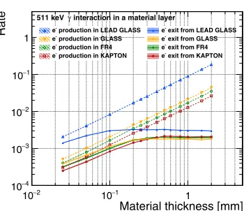
Figure 2. Interaction of a 511 keV photon in different materials, showing the normalised electron
production rate (dashed lines) and escape rate as function of the material thickness.
3 GEANT4 simulations for photon detection
Electrons produced by the conversion of photons in the thin amplification layers are simu-lated using GEANT 4 version 10.03 [6–8]. The physics list considered is FTFP_BERT_LIV. Figure 2 (dashed lines) shows the photon conversion rate for different materials (kapton, FR4, glass, and lead glass) as function of the thickness (25µmto 2mm). We use GEANT 4 ma-terials G4_KAPTON, G4_GLASS_PLATE and G4_GLASS_LEAD to define kapton, glass, and lead glass. FR4 (common PCB material) definition is implemented as 47.2% Epoxy and 53.8% SiO2. Electrons produced by photo-conversion can loose energy traversing the
con-verter material and can be stopped instead of reaching the gas. The rate of electron escaping the material thickness is shown in figure 2 (solid lines). One can observe that for each material the exiting rate saturates, where the higher probability for photon conversion is mitigated by a lower exit probability for early conversions. We consider the thinnest material to reach this plateau as the optimum thickness: e.g. 100µm for lead glass, resulting in a∼3%efficiency. For glass, FR4 and kapton the maximum efficiency is∼2%for materials of 300÷500µm thickness. Assuming Scheme B, a single stack (1mm) could consist of 300µm FR4 and 700µm gas. Hundred of such stacks would lead to a detector with thickness of only 10 cm and detection efficiency of 20%. An upper limit to the efficiency of the conversion layer in this scheme would be 40% (photon interaction rate of∼5%divided by the electron exit rate of∼2%).
The energy spectrum of the electrons in the drift region is shown in Figure 3 (left column) and can be used as input for the simulation of the primary ionization in the drift region and the avalanche in the gain region. The production energy at the moment of the photon conversion is shown in Figure 3 (right column) for the optimum thickness as defined earlier (all electrons: solid grey line, electrons reaching the gas: dashed grey line), together with the energy at the moment the electron escapes the material (colored solid line). Only the electrons with highest production energy can reach the gas while illustrating also the energy loss in the material.
4 Simulation of primary ionization and time resolution estimation
amplifica-Energy [MeV] 0 0.05 0.1 0.15 0.2 0.25 0.3 0.35 0.4
Electrons [a.u]
0 0.01 0.02 0.03 0.04 0.05 0.06
Material thickness 100 um 400 um 600 um 2 mm
interaction in KAPTON
γ
511 keV
Electron Energy [MeV] 0 0.05 0.1 0.15 0.2 0.25 0.3 0.35 0.4
Electrons
0 500 1000 1500 2000 2500 3000
all e
kin. prod
E
reaching gas
e
kin. prod
E
in gas
e
kin. entry
E
interaction in 400 um of KAPTON
γ
511 keV
Energy [MeV] 0 0.05 0.1 0.15 0.2 0.25 0.3 0.35 0.4
Electrons [a.u]
0 0.01 0.02 0.03 0.04
0.05 Material thickness100 um 300 um 600 um 2 mm
interaction in FR4
γ
511 keV
Electron Energy [MeV] 0 0.05 0.1 0.15 0.2 0.25 0.3 0.35 0.4
Electrons
0 500 1000 1500 2000
2500 all e -kin. prod
E
reaching gas
e
kin. prod
E
in gas
e
kin. entry
E
interaction in 300 um of FR4
γ
511 keV
Energy [MeV] 0 0.05 0.1 0.15 0.2 0.25 0.3 0.35 0.4 0.45 0.5
Electrons [a.u]
4
− 10
3
− 10
2
− 10
1
− 10
Material thickness 25 um 100 um 600 um 2 mm
interaction in LEAD GLASS
γ
511 keV
Electron Energy [MeV]
0 0.1 0.2 0.3 0.4 0.5
Electrons
1 10
2
10
3
10
4
10
5
10 all e -kin. prod
E
reaching gas
e
kin. prod
E
in gas
e
kin. entry
E
interaction in 100 um of LEAD GLASS
γ
511 keV
Figure 3. Electron energy distributions for (from top to bottom) kapton, FR4 and lead glass. The
left figure shows the energy distribution of the electrons exiting different material thicknesses, while
the right figure shows for a fixed thickness the kinetic energy at the production vertex for all electrons produced (solid grey line) and the subset of electrons escaping the material (dashed grey line), while the colored solid line shows the kinetic energy of the electron when entering the gas layer.
tion structure where they will be multiplied in an intense electric field, leading to a signal being picked up by external readout elements. The ionization pattern in the gas will
deter-mine the efficiency and time resolution of the signal. We have studied the primary ionization
with two different codes: HEED [9] and Garfield++ Microscopic Tracking [10]. HEED
implements the Photo-absorption ionization (PAI) model, splitting the atomic photoabsorp-tion cross-secphotoabsorp-tion into partial cross secphotoabsorp-tions for each subshell alowing in this way for atomic
relaxation effects. As such the program alows for a detailed simulation of the primary
Energy [MeV] 0 0.05 0.1 0.15 0.2 0.25 0.3 0.35 0.4
Electrons [a.u] 0 0.01 0.02 0.03 0.04 0.05 0.06 Material thickness 100 um 400 um 600 um 2 mm
interaction in KAPTON
γ
511 keV
Electron Energy [MeV] 0 0.05 0.1 0.15 0.2 0.25 0.3 0.35 0.4
Electrons 0 500 1000 1500 2000 2500 3000 all e kin. prod E reaching gas e kin. prod E in gas e kin. entry E
interaction in 400 um of KAPTON
γ
511 keV
Energy [MeV] 0 0.05 0.1 0.15 0.2 0.25 0.3 0.35 0.4
Electrons [a.u] 0 0.01 0.02 0.03 0.04
0.05 Material thickness100 um 300 um 600 um 2 mm
interaction in FR4
γ
511 keV
Electron Energy [MeV] 0 0.05 0.1 0.15 0.2 0.25 0.3 0.35 0.4
Electrons 0 500 1000 1500 2000
2500 all e -kin. prod E reaching gas e kin. prod E in gas e kin. entry E
interaction in 300 um of FR4
γ
511 keV
Energy [MeV] 0 0.05 0.1 0.15 0.2 0.25 0.3 0.35 0.4 0.45 0.5
Electrons [a.u] 4 − 10 3 − 10 2 − 10 1 − 10 Material thickness 25 um 100 um 600 um 2 mm
interaction in LEAD GLASS
γ
511 keV
Electron Energy [MeV]
0 0.1 0.2 0.3 0.4 0.5
Electrons 1 10 2 10 3 10 4 10 5
10 all e -kin. prod E reaching gas e kin. prod E in gas e kin. entry E
interaction in 100 um of LEAD GLASS
γ
511 keV
Figure 3. Electron energy distributions for (from top to bottom) kapton, FR4 and lead glass. The
left figure shows the energy distribution of the electrons exiting different material thicknesses, while
the right figure shows for a fixed thickness the kinetic energy at the production vertex for all electrons produced (solid grey line) and the subset of electrons escaping the material (dashed grey line), while the colored solid line shows the kinetic energy of the electron when entering the gas layer.
tion structure where they will be multiplied in an intense electric field, leading to a signal being picked up by external readout elements. The ionization pattern in the gas will
deter-mine the efficiency and time resolution of the signal. We have studied the primary ionization
with two different codes: HEED [9] and Garfield++ Microscopic Tracking [10]. HEED
implements the Photo-absorption ionization (PAI) model, splitting the atomic photoabsorp-tion cross-secphotoabsorp-tion into partial cross secphotoabsorp-tions for each subshell alowing in this way for atomic
relaxation effects. As such the program alows for a detailed simulation of the primary
ioniza-tion clusters along the trajectory of the original particle. Microscopic Tracking implements a rigorous tracking of the particle and all its daugther particles in the gas, sampling collisions with the gas molecules using the MAGBOLTZ [11] cross sections for elastic and inelastic collisions and excitation, ionization and attachment encounters. This method was originally
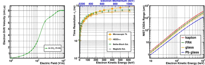
0 100 200 300 400 500 600 Electron Kinetic Energy (keV) 0 1 2 3 4 5 6 7 8 9 10 ) -1 g 2
Mass Stopping Power (MeV cm
Microscopic Tk
HEED++
NIST ESTAR
Bethe-Bloch
0200 400 600 800 1000 Electron Momentum (keV)
0 100 200 300 400 500 600 Electron Kinetic Energy (keV) 0 2 4 6 8 10 12 14 16 18 20
Cluster density (cls/mm)
Microscopic Tk HEED++ NIST Projected Bethe-Bloch Est. Magboltz Est. 0200 400 600 800 1000
Electron Momentum (keV)
Figure 4.Mass stopping power in a gas mixture of Ar:CO270:30 (left) and Cluster density (right)
sim-ulated by HEED (open circles) and Microscopic Tracking (full circles) confronted with NIST ESTAR data (grey full circles and dashed line) and Bethe-Bloch calculations (green open circles and dashed line).
implemented for the simulation of avalanches where the mean electron energy rarely exceeds a few hundred eV and has shown to provide reliable results in this energy range [12].
The simulations were validated against NIST ESTAR data for the energy loss in Ar:CO2 70:30 gas mixture. Figure 4 (left) shows the good agreement between Bethe-Bloch calcula-tions, NIST ESTAR data and HEED over the energy range 50-500 keV. Microscopic Tracking
has good agreement up to∼100 keV above which it under estimates the energy lost in the gas,
unable to reproduce the energy loss for a minimum ionising particle. Figure 4 (right) shows the number of clusters created by the ionizing particle along its trajectory. Here again, the ionization predicted by the Microscopic Tracking technique is slightly below the HEED pre-diction. As a cross check, we estimated the cluster density from theoretical Energy Loss
calculations (Bethe-Bloch) by dividing with the average energy to create aprimary
ioniza-tion (Wprim) in Ar:CO
2(70:30). Wprimwas estimated by confronting the energy loss in pure
Ar and CO2at minimum ionising energy (βγ =3.5) with precise measurements of the
spe-cific primary ionisation 2.3 cls/mm for Ar and 3.4 cls/mm for CO2 [13] and applyingBragg’s
rule, resulting inWprim =103.7 eV and 2.66 cls/mm for Ar:CO2 (70:30). Another estimate
of the cluster density was performed by inverting the mean free path for primary ionization:
NCls/mm = λ−I1 = (NσI)−1, using the weighted sum of the gross ionization cross section
of electrons on Argon and electrons on Carbondioxide, extracted from MAGBOLTZ. From both plots we can conclude that HEED has the best performance for the simulation of en-ergy loss and the simulation of primary ionization. Moreover, one can observe also that the curves of mass stopping power and cluster density have a similar logarithmic behaviour.
Plot-ting HEED dE/dxvs NCls/mm and applying this correction to the NIST dE/dx, a NCls/mm
estimate based upon NIST data was obtained and shown in Figure 4 (right).
The time resolution for a MPGD detector is determined by the drift velocity (vd) of the
electrons in the gas and the fluctuations of the distance of the closest electron to the amplifi-cation structure. The latter is given by the cluster density calculated earlier (Figure 4), while the former can be extracted from simple MAGBOLTZ simulations and is shown in Figure 5
(left). The occurence of ionisation clusters is a Poisson process and therefore the distanced
of the first ionisation cluster to the amplification structure follows an exponential distribution.
The arrival time is given by:t=d/vdand the time resolution is given by:σt=σd/vd=η/vd,
withηthe cluster density (η=NCls/mm=λ−I1), shown in Figure 5 (middle). Due to the high
2
10 103 104
Electric Field (V/m) 1
2 3 4 5 6 7 8
s)
µ
Electron Drift Velocity (cm/
(70:30)
2
Ar:CO
0 100 200 300 400 500 600 Electron Kinetic Energy (keV)
2
− 10
1
− 10
1 10
(ns)t
σ
Time Resolution Microscopic Tk
HEED++ Bethe-Bloch Est. Magboltz Est. 0200 400 600 800 1000
Electron Momentum (keV)
10 102 103
Electron Kinetic Energy (keV) 1
10
2
10
3
10
4
10
NIST CSDA Range (um)
kapton FR4 glass Pb glass
Figure 5.Left: Drift velocity as function of applied electric field in Ar:CO270:30 gas mixture. Middle:
estimated time resolution as function of electron kinetic energy for a single gas layer in Ar:CO270:30
gas mixture and 3 kV/cm drift field. Right: CSDA range of electrons in various materials.
of nearly 1 ns, while 100 keV and 350 keV electrons will have at best a time resolution of 2 and 4 ns respectively when detected in a single layer. Better time resolutions can be obtained by the FTM principle dividing the drift region (cfr. Figure 1). If the Compton electron is ener-getic enough to penetrate through several amplification structures, the fastest signal will than determine the detector time resolution. Using CSDA ranges from NIST, shown in Figure 5
(right), one can estimate that a 350 keV electron can penetrate at least 8 layers of 100µm
kapton, giving signal in 9 layers and leading to a time resolution of 4 ns/9=0.45 ns, while a
100 keV electron could about just penetrate 100µm kapton, leading to signals in two layers
and a time resolution of 2 ns/2=1 ns. The time resolutions might however be better, since if
a very soft (<50 keV), the time resolution will be defined by the ionization in this layer. The
time resolution might be further improved investigating gases and conditions (e.g. pressure) to increase the specific primary ionization and optimizing the material thicknesses.
5 Avalanche development
For the amplification structure of this detector we study the inverted cone geometry (50µm
top hole diameter and 70µm bottom hole diameter) of the Fast Timing MPGD, determined by
the etching procedure for the DLC coated polyimide. Figure 6 (left) shows the electric field
simulated with COMSOL in a single layer, with the anode at 500 V (100 kV/cm amplification
field) and cathode at 575 V (3 kV/cm drift field).
The electric field was simulated both with COMSOL and ANSYS. Figure 6 (right) demonstrates good agreement was found between the two Finite Element packages. A quick
estimation of the gain was obtained by integrating the extracted effective Townsend coeffi
-cient from Magboltz (with a correcting for the Penning effect [14, 15]) along a line in the
center of the hole:
G=exp h
0 αPen[E(z)] dz, αPen:
=α
1+rPenf
exc
fion
with fionthe direct ionization rate, fexcthe production rate of the excited argon states that
can ionise CO2andrPenthe Penning transfer rate, i.e. the probability that an excited Ar atom
ionizes a CO2molecule. This method was cross-checked by estimating the gain observed in
a similar wet-etched polyimide based detector [16] and good agreement was observed. A full
Microscopic Tracking simulation was performed in Garfield++simulating the avalanche
2
10 103 104
Electric Field (V/m) 1 2 3 4 5 6 7 8 s) µ
Electron Drift Velocity (cm/
(70:30)
2
Ar:CO
0 100 200 300 400 500 600 Electron Kinetic Energy (keV) 2 − 10 1 − 10 1 10 (ns)t σ
Time Resolution Microscopic Tk
HEED++
Bethe-Bloch Est.
Magboltz Est.
0200 400 600 800 1000 Electron Momentum (keV)
10 102 103
Electron Kinetic Energy (keV) 1 10 2 10 3 10 4 10
NIST CSDA Range (um)
kapton FR4 glass Pb glass
Figure 5.Left: Drift velocity as function of applied electric field in Ar:CO270:30 gas mixture. Middle:
estimated time resolution as function of electron kinetic energy for a single gas layer in Ar:CO270:30
gas mixture and 3 kV/cm drift field. Right: CSDA range of electrons in various materials.
of nearly 1 ns, while 100 keV and 350 keV electrons will have at best a time resolution of 2 and 4 ns respectively when detected in a single layer. Better time resolutions can be obtained by the FTM principle dividing the drift region (cfr. Figure 1). If the Compton electron is ener-getic enough to penetrate through several amplification structures, the fastest signal will than determine the detector time resolution. Using CSDA ranges from NIST, shown in Figure 5 (right), one can estimate that a 350 keV electron can penetrate at least 8 layers of 100µm kapton, giving signal in 9 layers and leading to a time resolution of 4 ns/9=0.45 ns, while a 100 keV electron could about just penetrate 100µm kapton, leading to signals in two layers and a time resolution of 2 ns/2=1 ns. The time resolutions might however be better, since if a very soft (<50 keV), the time resolution will be defined by the ionization in this layer. The time resolution might be further improved investigating gases and conditions (e.g. pressure) to increase the specific primary ionization and optimizing the material thicknesses.
5 Avalanche development
For the amplification structure of this detector we study the inverted cone geometry (50µm top hole diameter and 70µm bottom hole diameter) of the Fast Timing MPGD, determined by the etching procedure for the DLC coated polyimide. Figure 6 (left) shows the electric field simulated with COMSOL in a single layer, with the anode at 500 V (100 kV/cm amplification field) and cathode at 575 V (3 kV/cm drift field).
The electric field was simulated both with COMSOL and ANSYS. Figure 6 (right) demonstrates good agreement was found between the two Finite Element packages. A quick estimation of the gain was obtained by integrating the extracted effective Townsend coeffi-cient from Magboltz (with a correcting for the Penning effect [14, 15]) along a line in the center of the hole:
G=exp
h
0 αPen[E(z)] dz, αPen:
=α
1+rPenf
exc
fion
withfionthe direct ionization rate, fexcthe production rate of the excited argon states that
can ionise CO2andrPenthe Penning transfer rate, i.e. the probability that an excited Ar atom
ionizes a CO2molecule. This method was cross-checked by estimating the gain observed in
a similar wet-etched polyimide based detector [16] and good agreement was observed. A full Microscopic Tracking simulation was performed in Garfield++simulating the avalanche in-duced by a single electron in the drift gap. The charge distribution obtained with Garfield++
0 0.005 0.01 0.015 0.02 0.025 0.03
r (cm) 0 10 20 30 40 50 60 70 80 90 100
Electric Field (kV/cm)
Amplification Field FTM (140/70/50)
COMSOL ANSYS
20 kV/cm 30 kV/cm 40 kV/cm
50 kV/cm 60 kV/cm 70 kV/cm
80 kV/cm 90 kV/cm 100 kV/cm
0 50 100 150 200 250 300 350 400 450 500
Anode Potential (V)
Figure 6. Simulation of the electric field (V/m) in a single layer consisting of 250µm drift gap and
50µm high amplification structure with 50µm top hole diameter and 70µm bottom hole diameter and
140µm pitch (140/50/70) (left). Confrontation of the electric field (kV/cm) simulated with COMSOL
(solid line) and ANSYS (dashed line) for a the same structure, but now with top hole diameter 70µm
and bottom hole diameter 50µm (140/70/50) (right).
Entries 5000 Mean 3982 ± 47.82 Std Dev 3381 ± 33.81 Overflow 0
/ ndf 2
χ 80.8 / 75 Prob 0.3029
θ
Polya 0.9026 ± 0.0459 Gain 4545 ± 51.1 Const 236 ± 4.5
0 5000 10000 15000 20000 25000
Gain 1 10 2 10 3 10 Events
Entries 5000 Mean 3982 ± 47.82 Std Dev 3381 ± 33.81 Overflow 0
/ ndf 2
χ 80.8 / 75 Prob 0.3029
θ
Polya 0.9026 ± 0.0459 Gain 4545 ± 51.1 Const 236 ± 4.5 :: 32.98 %
2000e
≤
Gain
Entries 5000 Mean 3982 ± 47.82 Std Dev 3381 ± 33.81 Overflow 0
/ ndf 2
χ 80.8 / 75 Prob 0.3029
θ
Polya 0.9026 ± 0.0459 Gain 4545 ± 51.1 Const 236 ± 4.5
70:30 - Drift 3 kV/cm - Amp 100 kV/cm
2
FTM V4 - Ar:CO
100 200 300 400 500 600
Anode Potential (V) 1 − 10 1 10 2 10 3 10 4 10 5 10 Gain
70:30 - Drift 3 kV/cm - Amp 20-120 kV/cm
2
FTM V4 - Ar:CO
GARFIELD Sim w/ Penning
COMSOL Sim w/ Penning
GARFIELD Sim w/o Penning
COMSOL Sim w/o Penning
Figure 7.Charge distributions simulated with Garfield++for 100 kV/cm (left) and comparison between
Gain simulated with Garfield++and estimated with COMSOL (right).
with amplification field at 100 kV/cm and drift field at 3 kV/cm is shown in Figure 7 (left). The observed spectrum is fitted with a Polya distribution, Figure 7 (right) shows the agree-ment between the gain estimated with COMSOL and simulated with Garfield++. Perfect agreement is obtained when the Penning effect is not taken into account, a small difference however occurs when corrections for the Penning effect are taken into account.
6 Conclusion
of multiple detection layers could lead to a time resolution of 0.5 ns, to improve further on the time resolution, more detailed simulations are required, optimizing primary ionization and material thicknesses.
7 Acknowledgements
We are thankful to Dr. R. Veenhof for valuable suggestions and to INFN for supporting the research on the FTM through the grant for young researchers “MPGD_FaTimA”.
References
[1] M. Titov and L. Ropelewski, Micro-pattern gaseous detector technologies and
RD51 Collaboration, Mod.Phys.Lett. A28 (2013), 1340022. dx.doi.org/10.1142/
S0217732313400221.
[2] R. De Oliveira, M. Maggi, A. Sharma,A novel fast timing micropattern gaseous
detec-tor: FTM., arXiv:1503.05330[physics.ins-det] (2015). https://arxiv.org/abs/1503.05330.
[3] T. Papaevangelou, et al.,Fast Timing for High-Rate Environments with Micromegas, PJ
Web Conf. 174 (2018) 02002. 10.1051/epjconf/201817402002.
[4] M. Conti, State of the art and challenges of time-of-flight PET, Physica Medica 25
(2009) 1-11. dx.doi.org/10.1016/j.ejmp.2008.10.001.
[5] T.K. Lewellen,Recent developments in PET detector technology, Phys. Med. Biol. 53
(2008) R287. dx.doi.org/10.1088/0031-9155/53/17/R01.
[6] S. Agostinelli, et al.,GEANT4: A Simulation toolkit, Nucl. Instrum. Meth. A506 (2003)
250-303. dx.doi.org/10.1016/S0168-9002(03)01368-8.
[7] J. Allison et al., Geant4 Developments and Applications, IEEE Trans. Nucl. Sci. 53
(2006) 270-278. dx.doi.org/10.1109/TNS.2006.869826.
[8] J. Allison et al., Recent developments in GEANT4, Nucl. Instrum. Meth. A835 (2016)
186-225. dx.doi.org/10.1016/j.nima.2016.06.125.
[9] I.B. Smirnov,Modeling of ionization produced by fast charged particles in gases. Nucl.
Instrum. Meth. A554 (2005) 474-493. dx.doi.org/10.1016/j.nima.2005.08.064.
[10] H. Schindler,Microscopic Simulation of Particle Detectors. CERN-THESIS-2012-208.
cds.cern.ch/record/1500583.
[11] S.F. Biagi, Monte Carlo simulation of electron drift and diffusion in counting gases
under the influence of electric and magnetic fields. Nucl.Instrum.Meth. A421 (1999)
234-240. dx.doi.org/10.1016/S0168-9002(98)01233-9.
[12] H. Schindler et al., ] Calculation of gas gain fluctuations in uniform fields.
Nucl.Instrum.Meth. A624 (2010), 78-84. dx.doi.org/10.1016/j.nima.2010.09.072.
[13] F.F. Rieke and W. Prepejchal, Ionization Cross Sections of Gaseous Atoms and
Molecules for High-Energy Electrons and Positrons. Phys. Rev. A 6, 1507. dx.doi.org/
10.1103/PhysRevA.6.1507.
[14] O. Sahin et al.,Penning transfer in argon-based gas mixtures. Journal of Instrumentation
5 (2010) P05002 1-30. dx.doi.org/10.1088/1748-0221/5/05/P05002.
[15] O. Sahin et al.,High-precision gas gain and energy transfer measurements in Ar-CO2
mixtures.Nucl.Instrum.Meth. A768 (2014) 104-111. dx.doi.org/10.1016/j.nima.2014.
09.061
[16] G. Bencivenni et al.,The micro-Resistive WELL detector: a compact spark-protected
single amplification-stage MPGD. JINST 10 (2015) P02008. dx.doi.org/10.1088/