ABSTRACT
KUMAR, SEEMA. Memory Design for Sensor IC. (Under the direction of Dr. P. D. Franzon.)
Sensors are finding application in areas like agriculture and food science and low power
operation is often a key requirement. Since memory is a substantial component of these sensor
systems, a low power memory design can be a significant contribution towards meeting the
power budget.
This work presents a memory design for a sensor IC with emphasis on low power. The
memory was designed in Chartered 0.13µm Low Power process. The designed memory provides
300 bytes of storage with an average read current of 701.5µA and average write current of 190.21
µA. The memory has a total area of 390.46µm x 396.28 µm, read access time is 251.7 ns and
write time is 12.776 ns.
In addition to the design of the actual storage part of the memory, this work also presents
Memory Design for Sensor IC
by Seema Kumar
A thesis submitted to the Graduate Faculty of North Carolina State University
in partial fulfillment of the requirements for the Degree of
Master of Science
Computer Engineering
Raleigh, North Carolina
2010
APPROVED BY:
Dr. W. R. Davis Dr. J. M. Wilson
DEDICATION
BIOGRAPHY
Seema Kumar received her B.E. degree (with honors) in Electronics and Communication
En-gineering (ECE) from Birla Institute of Technology, Mesra, Ranchi, India in June 2001. Her
undergraduate project work was focused on analog filter design for Digital Subscriber Line
(DSL) systems.
From June 2001 to January 2003, she worked as a Software Engineer at HCL Technologies
Ltd. in Gurgaon, India where she was involved with benchmarking of synthesis related EDA
tools. From January 2003 to September 2003, she worked as a Design Engineer at NeoMagic
Semiconductor (I) Pvt. Ltd. Noida, India where she was involved with design of modules related
to video capture and rendering, test and virtual prototyping. From October 2004 to March 2007
she worked as a Senior Design Engineer at SiRF Technologies (I) Pvt. Ltd, Noida, India. At
SiRF she was involved with the design of ARM based SoC for GPS/Bluetooth applications.
Since August 2008, she has been working towards her Master’s degree in the field of
Com-puter Engineering at NC State University. Her main research interests include comCom-puter systems
design, ASIC and VLSI design, CAD methodology and automation, SoC design and low power
design techniques.
Ms. Kumar is a student member of IEEE, IEEE Solid State Circuits Society, IEEE
Com-puter Society, and a member of the local NCSU chapter of IEEE Women in Engineering. She
ACKNOWLEDGEMENTS
First and foremost I would like to thank my advisor Dr. Paul Franzon for giving me the
opportunity to work in his group. I am grateful for his guidance and his unique manner of
advising that nurtures the spirit of exploration. I would also like to express my gratitude to
my committee members, Dr. Rhett Davis and Dr. John Wilson for helping me with guidance
and advise from time to time.
I had the privilege of working and interacting with various researchers in Dr. Franzon’s
research group and it has been a great educational experience. First of all I would like to thank
Dr. Steve Lipa for his generous explanations and answers to all my questions, no matter how
silly they were. Thanks to Akalu for being a mentor and believing in me enough so as to let me
be a part of his design. Thanks to Thor for always answering my questions any time. Thanks
to Bruce Su, Chanyoun Won, Samson Melamed, Chris Mineo and Hoon Seok for answering my
questions from time to time. Thanks to Evan for helping me with IT resources.
Thanks to the wonderul faculty of the ECE department that make each class an enriching
experience.
Thanks to the wonderful ladies at the ECE graduate office - Ms. Hardin and Ms. Wilson
for being ever helpful and kind. Thanks to Ms. Patsy at MRC for her generous help.
Thanks to all the members of my family for being ever supportive and encouraging. Last
but not the least, I would like to express my gratitude to my husband, Jayesh, without whose
financial help and emotional encouragement, I would never ever have been able to attend
TABLE OF CONTENTS
List of Tables . . . vii
List of Figures . . . .viii
Chapter 1 Introduction . . . 1
1.1 Sensors . . . 1
1.2 Process Technology . . . 2
1.3 Thesis Organization . . . 3
Chapter 2 Requirements . . . 4
2.1 System Description . . . 4
2.1.1 Write Mode Operation . . . 5
2.1.2 Read Mode Operation . . . 5
2.2 Memory System Description . . . 7
2.2.1 Memory System Interface Signals . . . 8
2.3 Summary . . . 10
Chapter 3 Memory System Design . . . 11
3.1 Memory Interface . . . 11
3.1.1 Address Generation . . . 12
3.1.2 Mode Determination . . . 13
3.1.3 Write Data Gating . . . 13
3.2 Memory Interface Implementation . . . 14
3.2.1 Design . . . 14
3.2.2 Verification . . . 14
3.2.3 Synthesis and Physical Design . . . 15
Chapter 4 Memory Array Design . . . 17
4.1 Low Power and Low Energy Design Schemes . . . 17
4.1.1 Lower Operating Voltage . . . 17
4.1.2 Use of Static Circuits . . . 18
4.1.3 Use of Sense Amplifiers . . . 18
4.1.4 Use of Divided Word Lines . . . 19
4.1.5 Layout Considerations . . . 20
4.2 Memory Array . . . 21
4.2.1 Bitcell . . . 21
4.2.2 Decoder and Column Mux . . . 24
4.2.3 Write Path . . . 25
4.2.4 Read Path . . . 25
4.2.5 AND Gate for Divided Word Line . . . 31
4.2.7 Total Memory Array . . . 32
4.3 Simulation Results . . . 32
4.3.1 Static Noise Margin (SNM) . . . 32
4.3.2 Write Noise Margin (WNM) . . . 38
4.3.3 Leakage Current . . . 40
4.3.4 Write Operation . . . 42
4.3.5 Read Operation . . . 42
4.4 Power Analysis . . . 44
Chapter 5 Future Work . . . 45
Chapter 6 Conclusion . . . 47
References. . . 48
Appendices . . . 50
Appendix A Memory Interface Design Files . . . 51
A.1 Verilog - Memory Inteface Top . . . 51
A.2 Verilog - Memory Interface . . . 59
A.3 Verilog - Integrated Decoders . . . 65
A.4 Verilog - Decoder . . . 69
Appendix B Memory Interface Tool Script Files . . . 72
B.1 Design Compiler Scripts . . . 72
B.2 SoC Encounter Script - Configuration File . . . 75
B.3 SoC Encounter Script - Placement File . . . 77
B.4 SoC Encounter - CTS Files . . . 78
B.5 SoC Encounter - Pin Placement File . . . 79
Appendix C Memory Interface Verification Files . . . 82
C.1 Verilog Test Bench . . . 82
LIST OF TABLES
Table 2.1 Memory Interface Signals Description . . . 9
LIST OF FIGURES
Figure 1.1 Tezzaron Tier Stack-up . . . 2
Figure 2.1 System Block Diagram . . . 4
Figure 2.2 Main System State Machine . . . 6
Figure 2.3 Memory System Interface Signals . . . 10
Figure 3.1 Top Level View of Address Generation Logic . . . 12
Figure 3.2 Timing Diagram for Read Done and Write Done Signals . . . 13
Figure 4.1 Divided Word Line Scheme [10] . . . 20
Figure 4.2 Bitcell Schematic . . . 22
Figure 4.3 Bitcell Layout . . . 23
Figure 4.4 Layout of Memory Interface, Decoder and Column Mux . . . 26
Figure 4.5 Write Path Schematic . . . 27
Figure 4.6 Write Path Layout . . . 28
Figure 4.7 Read Path Schematic . . . 29
Figure 4.8 Read Path Layout . . . 30
Figure 4.9 AND Gate Schematic . . . 31
Figure 4.10 AND Gate Layout . . . 32
Figure 4.11 Pre-Charge Schematic . . . 33
Figure 4.12 Pre-Charge Layout . . . 34
Figure 4.13 Memory System Arrangement . . . 35
Figure 4.14 Array Layout . . . 36
Figure 4.15 Integrated Memory System Layout . . . 37
Figure 4.16 Measuring Static Noise Margin [12] . . . 38
Figure 4.17 Static Noise Margin, 25◦C . . . 39
Figure 4.18 Static Noise Margin, 100◦C . . . 39
Figure 4.19 Measuring Write Noise Margin [12] . . . 40
Figure 4.20 Write Noise Margin, 25◦C . . . 41
Figure 4.21 Write Noise Margin, 100◦C . . . 41
Figure 4.22 Write - Operation and Access Time, 25◦C . . . 43
Chapter 1
Introduction
1.1
Sensors
Sensors are a ubiquitous part of our lives today. They can be as simple as the control system for
maintaining the oven temperature in the kitchen to as complex as providing real time missile
navigation. Whether they are used in a control system or as a simple data logger, a sensor can
be partitioned into canonical functional units as described next.
The frontend of the sensor consists of the sensing device. This is the part responsible for
sensing the parameter of interest like temperature, pressure or orientation and converting it into
an electrical quantity like a voltage or current. This generated voltage or current can then be
processed further to be represented in a form that is more amenable to digital signal processing
or storage. In a control system, the processed signal can then be used to generate actuator
signals to control some part of the design. In a data logging system, the converted data may
scaled or compressed and written into memory to be accessed and analyzed later. Even control
systems may do data logging for later analysis or debugging.
In addition to the aforementioned basic units, no system can work without a power supply.
For some applications, a convenient source of power may be available for use, but for sensors that
there also needs to be an interface in the system to facilitate data retrieval from the data
memory or implement a command interface. This could be in the form of a standard wired
communication interface like the USB or a wireless interface like RFID.
Advancement in semiconductor fabrication and processing technology has made adoption
of sensors in unconventional areas commonplace. Sensors are now finding use in the fields of
agriculture and food science. Development of 3DIC technology also opens up exiting potential
for developing a system that can be contained in a single package, with different tiers being
used for logic, memory, storage capacitors etcetera. The work documented in this thesis is a
part of sensor design targeted to such a process. The following section describes the target
process technology.
1.2
Process Technology
The target technology for this work is Chartered 0.13 µm Low Power process. The stack-up
provided by Tezzaron [17] is shown in Figure 1.11
Figure 1.1: Tezzaron Tier Stack-up
There are two logic layers that can then optionally be connected to a DRAM layer. This
design does not require the DRAM layer, hence no TSVs are required for connection of logic
to memory. However, a certain TSV density is required for manufacturing processes.
For this design, the entire logic, including the memory, is contained in a single layer, hence
no TSVs are required for either logic to logic or logic to memory connections. The unused logic
layer has been used to implement large storage capacitors. The area of the entire design is 2.5
mm x 5 mm.
1.3
Thesis Organization
Chapter 2 starts with a description of the system operation at the top level. From that
descrip-tion, the requirements for the memory block are determined. Chapter 3 discusses the memory
interface design. in that, the various functions of the memory system, the design and physical
ipmlementation of the memory system interface are discussed. Chapter 4 presents the design
of the storage part of the memory. Various schemes for low power design are discussed. The
design, both schematic and layout of various elements of the memory are described followed by
the description of the fully array design. Simulation results are also presented in this chapter.
Chapter 2
Requirements
This chapter gives a brief description of the operation of the entire system. From that top level
functional description, the requirements for the memory block are determined.
2.1
System Description
The sensor IC is targeted to be used in food processing as a temperature logger. The sensor is
to be put along with food particles to determine the temperature that the particles are exposed
to in a particular process. The measured temperature is to be stored in a memory array and
later read out for analysis. The top level operation of the sensor can be understood with the
help of Figure 2.1. A temperature sensor senses the temperature at the front end, the ADC
converts the voltage equivalent of the measured temperature to an 8-bit value which is then
written into the memory. Once data collection is complete, data is read out of the memory using
an RFID interface controlled by an external RFID reader. The power system is responsible for
generating the supply voltage for various blocks and also consists of a charging circuit and
storage capacitor. The clock and reset block is responsible for generating the required clock
frequencies and their associated resets.
This system, therefore, has two distinct modes of operation, which are
-1. Data collection mode where the memory is written into.
2. Data retrieval mode where memory contents are read.
The following section look at these two modes and operation in these modes.
2.1.1 Write Mode Operation
In this mode, temperature is sensed, converted to an 8-bit value which is written into the
memory. The sensing frequency is 1 Hz, that is one sample is collected every second. The data
is written in sequential locations in the memory and there is no reading of memory. Since no
other blocks are active in this mode, it is the responsibility of the memory system to generate
any and all required signals for writing.
2.1.2 Read Mode Operation
In this mode, the data written in the memory is retrieved using an RFID interface, with an
RFID reader acting as the master. In order to comply with the RFID interface implementation,
the read address is provided to the memory by the RFID interface. Even though actual memory
access during reading is expected to be sequential, the address is provided by the RFID interface.
location is accessed at a fixed interval of time determined by the 1 Hz clock, reading needs takes
into account the time required for acknowledgement and re-transmission before moving on to the
next location. Memory is read at a frequency of 2 MHz. This refers to the read clock frequency,
however a new location may not be read at the rate of 2 MHz, but at a rate determined by
acknowledgement and re-transmission status between the sensor and the RFID reader.
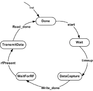
The entire system is controlled by a top level state machine that is shown in Figure 2.2.
Five states are identified
-Figure 2.2: Main System State Machine
• Done: This state indicates that the sensor has completed one write and read cycle and
• Wait: Once the sensor needs to start writing data again, there is a wait period from the
time that it is known that write needs to begin and for the actual write to begin. This
state indicates that the sensor system is in that wait cycle. Currently it is set at 3 minutes
by a hardware counter. Once the hardware timer indicates that the set time has elapsed,
the system progresses to theDataCapture state.
• DataCapture: This is the actual write state. In this state the memory system is writing
data at the rate of one 8-bit data element every second. When the entire memory array
has been written once, the memory system generates a signal indicating that write has
been done. The system then progresses to the stateWaitForRF
• WaitForRF: This is the state between writing data and the reading to begin. The sensor
system waits for an RF incidence to start the read phase. Till the time that there is no
RF presence, the system remains in this state. When RF energy is detected, the system
progresses to the state TransmitData.
• TransmitData: This is the actual read state. Addresses generated by the RFID interface
are read. These addresses are expected to be sequential, but read from a new location is
not expected to happen every clock cycle. Once all the locations are read, the memory
system generated a signal indicating this and the main state machine progresses to the
stateDone, where it remains till the next cycle starts.
The memory system is to read the state machine state and accordingly generate signals for read
and write. Additionally, the memory system is also required to generate signals to be used by
this main state machine to indicate when the entire memory array has been written to or read
from.
2.2
Memory System Description
follows-Once the system is in the write mode, the memory system needs to generate sequential
addresses every 1 second and store the data on its input data lines. The memory does not read
any location in this mode. Once all the memory locations are written into, it needs to generate
a signal indicating this status. It does not overwrite data once the entire array has been written
once.
In the read mode, a read address is provided by the RFID interface. The address indicated
by the read address is read by the memory. The read address is changed depending on whether
the same location needs to be re-read or not. The memory system does not need to generate
addresses internally in this mode. The memory system, however, does need to generate a signal
indicating all the locations have been read for use by the main state machine.
Required Memory Capacity: The system requires that at least 5 minutes of temperature
data needs to be stored in the memory. This sets the total number of storage bits to be at least
equal
to-(5 x 60) seconds x 8-bits = 2400 bits
These bits are organized in bytes and each addressable location is byte wide. Thus there
need to be at least 300 addressable locations.
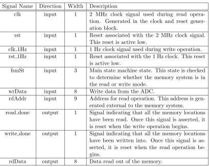
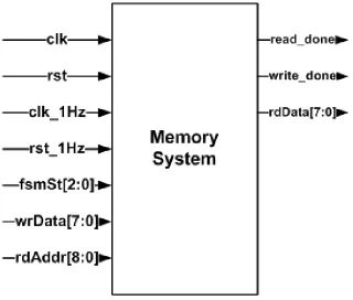
2.2.1 Memory System Interface Signals
Figure 2.3 shows all the interface signals of the memory system. Although the memory system
has two clocks, only one is active at a time. During reads, only the 2 MHz clock is running
and during writes only the 1 Hz clock is running. This gating is implemented external to the
Table 2.1: Memory Interface Signals Description
Signal Name Direction Width Description
clk input 1 2 MHz clock signal used during read
opera-tion. Generated in the clock and reset gener-ation block.
rst input 1 Reset associated with the 2 MHz clock signal.
This reset is active low.
clk 1Hz input 1 1 Hz clock signal used during write operation. rst 1Hz input 1 Reset associated with the 1 Hz clock. This reset
is active low.
fsmSt input 3 Main state machine state. This state is checked
to determine whether the memory system is in the read or write mode.
wrData input 8 Write data from the ADC.
rdAddr input 9 Address for read operation. This address is gen-erated external to the memory system.
read done output 1 Signal indicating that all the memory locations have been read. Once this signal is asserted, it is reset when the write operation begins. write done output 1 Signal indicating that all the memory locations
have been written into. Once this signal is as-serted, it is reset when the read operation be-gins.
Figure 2.3: Memory System Interface Signals
2.3
Summary
The memory needs to have at least 2400 bits and should be byte addressable. The memory
does fully array write followed by a full array read. The write and read modes of the memory
are controlled by the main state machine states. During write operation, memory system needs
to generate addresses internally. Read address is provided as input. Once the entire array has
either been read or written to, a signal indicating this needs to be generated by the memory
system. The memory system needs to be able to store at least 5 minutes of sensed data. Write
operation needs to run off of a 0.3 mAh battery requiring the memory to be low energy. Of the
total available area of 5 mm x 2.5 mm, the entire memory system needs to fit into a maximum
Chapter 3
Memory System Design
As mentioned in Chapter 2, the memory system needs to generate its own addresses when it
is in the write mode and use the addresses provided by the RFID interface in the read mode.
This enables the division of the memory system into two distinct modules
-• Memory Interface: This module interfaces the actual storage part of the memory with
the rest of the logic and performs address generation during write mode. The function
and design of this module is covered in Section 3.1.
• Memory Array: This is the actual storage memory with bitcells for storing data. It does
not directly interface with the rest of the system design, but rather through the Memory
Interface. The design of the memory is covered in Chapter 4
3.1
Memory Interface
This module interfaces the actual memory with the rest of the logic. It carries out the following
2. Mode Determination
3. Write Data Gating
The following sections discuss these functions in detail.
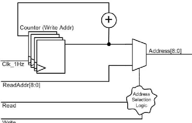
3.1.1 Address Generation
The internal address generation requirement for writes is handled by this module. It also takes
in the provided address for reads and multiplexes it with the write address so that only one
address is presented to the actual memory.
Write address generation is done using a counter that is active only in the write mode as
determined by the logic described in section 3.1.2.
Figure 3.1: Top Level View of Address Generation Logic
Figure 3.1 shows the top level logic implementation of this function of the memory interface.
3.1.2 Mode Determination
Additionally, this module also has the logic to determine whether the memory system is
cur-rently in the read or write mode based on the main state machine state. This module also
generates the read and write done signals that are consumed by the main state machine.
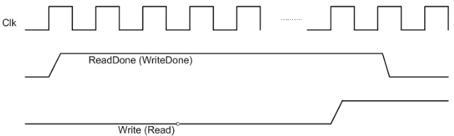
Write Done Signal
Write done signal is generated off the 1 Hz clock and has the timing as sown in Figure 3.2. This
signal is asserted when the last address is being written to and is de-asserted when the read
signal is asserted.
Read Done Signal
Read done signal is generated off the 2 MHz clock. It indicates that the last memory location
has been read at least once. Assertion of the read done signal does not indicate that the
mem-ory cannot be read any more. Read operation on the memmem-ory can still happen. Re-reading of
the last memory location may be required even after read done signal is asserted is a negative
acknowledgement is received from the RFID reader. The read done signal has the same timing
as shown in Figure 3.2.
Figure 3.2: Timing Diagram for Read Done and Write Done Signals
3.1.3 Write Data Gating
This module is also responsible for gating and registering the write data before it is presented
is directly generated by the output of the analog to digital converter (ADC). The used ADC
is a successive approximation type ADC, so the actual write data is known only after all the
cycles of approximation, which is eight cycles per sample for the case of a 8-bit ADC. The data
value may change during approximation cycles. If not gated, every time the data changes, the
changed data will be written to the memory resulting in numerous charging and discharging
cycles of the bitlines. Since data is repeatedly over-written and the correct and relevant data is
only the final data, which is available every 1 second, only that data is registered and presented
to the memory write data lines. This reduces useless data writes and saves on power. Since
the clock used by the memory system for write itself is 1 Hz, registering the data output of the
SAR using this clock performs both gating and registering of data.
3.2
Memory Interface Implementation
3.2.1 Design
The memory interface was implemented in Verilog HDL. Appendix A.1 has the HDL for this
module.
The 1 Hz and 2 MHz clock are not active simultaneously. The 1 Hz clock is active only
during writes and the 2 MHz clock is active only during reads. Also the logic running off of
the two clocks does not communicate, hence there is no need for any synchronization or hand
shaking in the logic.
3.2.2 Verification
The verification was done using a simple unit level verilog based testbench. Modelsim was used
3.2.3 Synthesis and Physical Design
The design was synthesized to the available Chartered 0.13 µm library with normal Vt. The
design compiler script for synthesis is presented in Appendix B.1. The design was synthesized
to 2 MHz for both the clocks to ensure that the setup time is met for both the read and
write modes. The synthesized netlist was then taken through the place and route flow with
Cadence’s SoC Encounter. The script used for SoC Encounter is presented in Appendix B.2
and Appendix B.3.
Clock tree synthesis was done for both the clocks using SoC Encounter. The script
con-trolling the CTS engine of SoC Encounter is presented in Appendix B.4. The physical verilog
netlist was written out of SoC encounter to run through Mentor Graphic’s v2lvs tool for LVS
check. Following is the command that was used for v2lvs
-v2lvs -lsp /afs/eos.ncsu.edu/lockers/research/ece/dk_tezzaron/\
CharteredLibsLP032309/FB/aci/sc-x/lvs_netlist/csm13lp.cdl -o \
mem_if.sp -s /afs/eos.ncsu.edu/lockers/research/ece/dk_tezzaron/\
CharteredLibsLP032309/FB/aci/sc-x/lvs_netlist/csm13lp.cdl \
-s0 VSS -s1 VDD -v mem_if_phys.v
Before running v2lvs, it was ensured that there were no nets in the verilog netlist with only
case difference. Since verilog is case insensitive and hspice is case sensitive, net names that only
have a case difference like ’n1’ and ’N1’ are distinct in verilog but are the same in hspice. Since
this makes LVS impossible, any occurrence of such net names was corrected before running
the netlist through v2lvs. The resulting CDS netlist was used as the schematic against which
the streamed gds was checked in LVS. Although this step may seem redundant given that an
automatic place and route tool was used, errors were seen to occur in routing with power lines
shorted to signal lines. The gds was also run through DRC to check for any any design rule
violations.
In order to make the final integration easier, the pin placement was manually controlled using
Chapter 4
Memory Array Design
This chapter discusses the design of the memory array. Low power schemes investigated for the
design are discussed in the beginning followed by a description of the design details.
4.1
Low Power and Low Energy Design Schemes
The emphasis on the design of this memory is low energy as it needs to operate on a 0.3 mAh
battery for the entire write operation. Since the operating frequency of this design is quite low,
more emphasis is on low energy and static power. But the design also needs to ensure that the
current drawn during switching process is within the bounds of the power budget.
This section discusses the various techniques presented for low power design in literature.
4.1.1 Lower Operating Voltage
Current is drawn by a circuit when it is switching leading to dynamic power consumption and
also when it is not switching leading to static power consumption[13]. The dynamic energy
consumption is approximated by
where, C is the switching capacitance and Vdd is the supply voltage.
Additionally, the static power consumption is approximated
by-PSta =V dd•Ileakage (4.2)
The leakage current itself is a function of the supply voltage.
From the equations of both static and dynamic power/energy, it is obvious that a low Vdd is
beneficial for low energy design. This scheme for reducing energy consumption is also discussed
in [3] . The memory is therefore designed to be operated off of a supply of 0.9 V as opposed to
the 1.5 V nominal supply voltage for the process. 0.9 V is the lowest supply voltage available
in the system. The nominal threshold voltage of the devices is 0.3 V. Therefore, the system can
operate with a supply voltage of 0.9 V. The drawback of using a lower supply voltage is slower
circuit operation [9], but since the design does not need to operate at high frequencies, there is
no need for a higher supply voltage to meet timing requirements.
4.1.2 Use of Static Circuits
Dynamic circuits require a clock for proper operation and switch every clock cycle irrespective
of whether the inputs change. This results in extra power consumption as compared to static
circuits that switch only when the input changes. As discussed in [9, 16], dynamic circuits are
typically used in paths that are timing critical. Dynamic circuits can switch very fast at the cost
of additional power consumption and are typically found in micro-processor data paths that
are timing critical. Since high speed operation is not a requirement for this design, dynamic
circuits are not a suitable option. Thus the decoder and column muxes for the memory have
been designed using static circuits.
4.1.3 Use of Sense Amplifiers
Sense amplifiers are often used in large SRAM circuits for increased read speed and robustness.
Since the read frequency for the memory is not high and the memory array is not large,
sense amplifiers are not strictly required. The fact that sense amplifiers are not strictly required
for SRAM read operation is also discussed in [9, 10]. Thus the memory design does not use
sense amplifier for read. Additionally, if there are no sense amplifiers, both the bitlines do not
need to be pre-charged for read operation, which results in extra power saving during read.
From the perspective of the entire design, not having a sense amplifier obviates the need for
a complicated balanced pre-charging circuit. A very sipmle PMOS based pre-charging circuit
may be used instead.
4.1.4 Use of Divided Word Lines
As seen in the equation for dynamic energy, the amount of energy expended is directly
propor-tional to the capacitance being charged. Thus a lower value of the load capacitance is in the
interest of the low power design. Additionally, since the supply voltage of the design has been
lowered, a lower load capacitance ensures that switching speed is not impacted.
The total capacitance that needs to be charged for a given read or write cycle consists of
the capacitance presented by the word line as well as the bitlines. Since all the columns are not
accessed at the same time, the word line for the bitcells not belonging to the accessed column
need not be driven. This observation is used to create a word line structure called the divided
word line. This structure is shown in Figure 4.11. The basic scheme is shown in [7, 10]. The total capacitance of the word line driven by the decoder is substantially reduced as all the access
transistors are not connected to the main driven wordline. The actual word line of only the
accessed column is driven.
This scheme has been implemented in the memory to reduce dynamic current consumption
of driving the wordline. The reduction in dynamic current comes from reduced word line
capacitance and the fact that bitline current flows only in the selected word [7]. This scheme
has been shown to reduce the bitline current by 7/8th the original value in [7]. In terms of
Figure 4.1: Divided Word Line Scheme [10]
the reduction in capacitance, for a row of 40 bitcells, the load on the wordline consists of the
wire capacitance as well as 80 gate capacitances. The length of the wordline is not reduced by
implementing divided word line as additional AND gates are introduced in a row. The gate
capacitance, however is reduced as for a word of 8 bits, the main wordline now has a load of
20 gates capacitances only in addition to the wire capacitance. The secondary wordline driving
the actual bitcell access transistors has a load of 16 gate capacitances in addition to the wire
capacitance.
4.1.5 Layout Considerations
Good layout can result in substantial reduction in capacitance and hence can help in lowering
the dynamic power consumption of the circuit. Some of the layout guidelines to keep in mind
are [15]
-• Create a compact layout for basic cells.
• Try to keep the aspect ratio of the memory unity to have the smallest bitline and wordline
length.
• Used multiple fingers with shared source/drain for large devices - This helps in
substan-tially reducing drain capacitance.
• Plan layout such that lines such as wordlines and bitlines can connect on abutment - This
reduces additional length on these lines for connection.
• Plan I/O port placement such that they can also connect on abutment to reduce
connec-tion length.
• Do not run metal lines from adjacent layers on top of each other. Use orthogonal routing
direction for adjacent metal layers. This scheme is the most important rule to follow to
reduce coupling capacitance and also helps in reducing system noise due to crosstalk.
4.2
Memory Array
This section describes the design of the elements of the memory array and the final array itself.
4.2.1 Bitcell
Bitcells occupy the largest area of the memory and hence should be as small as possible. In
the interest of small bitcells, designs described in [2] were evaluated. Four transistor bitcells,
as presented in [2], were small in terms of the number of transistors, but were quasi-static in
operation. This meant that the value stored in the bitcell had limited life time and if not
accessed within that lifetime, it would be lost. In order to keep the value in the bitcell for a
longer duration, a scheme similar to a DRAM refresh needed to be implemented. Since in this
design, the value stored in the bitcell had to be stable for times in the order of seconds, this
type of bitcell was not a viable option.
The standard six transistor cell was the best option for this design as it is completely static
and does not require any refresh to retain stored value. It consists of a pair of cross-coupled
inverter pairs that act as a static storage element. Data is written to and read from the bitcell
Figure 4.2: Bitcell Schematic
The schematic of the bitcell is presented in Figure 4.2. For write operation, the wordline
of the addressed bitcell is asserted to switch on the access transistors and the data value to
be written and its inverse are asserted on the bitline and bitline bar respectively. For read
operation, the bitlines are first pre-charged to VDD and then the wordline is asserted to switch
on the access transistors. Depending on the whether the value stored in the bicell is a ’1’ or
a ’0’, the pre-charged bitline either remains at the precharged value of VDD, or discharges to
ground. A single bitline is sufficient to read out a bitcell value.
In order to reduce leakage from the bitcell, larger length devices were used in the
cross-coupled inverter pair and the bitcell was simulated to ensure correct read and write operation.
The requirement of small area of the bitcell was realized through careful layout. Figure 4.3
shows the layout. The dimensions of the layout are 3.86 µm by 4.6650 µm. The bitlines and
wordlines were laid out such that bitcells would connect on abutment. Also the VDD and GND
rails were layed out to ensure they could be shared. Abutment and sharing ensures that the
4.2.2 Decoder and Column Mux
A decoder is required to translate the address to the assertion of the appropriate wordline and
the column mux is required to translate the address to the assertion of the appropriate column
select signal. During write mode, a decoder is not strictly required, as the memory is accessed
in sequence and that too with a definitive timing interval. Hence a full fledged decoder does
not need to be implemented for asserting wordlines. Such a scheme is also discussed in [1].
During read mode, even though the read addresses are provided by the RFID interface, they
are expected to be sequential. But the sequence timing is not fixed and is not deterministic.
That makes the use of shift registers for wordline assertion during read a non-viable option
without any additional logic. Additional logic may be implemented with the shift register that
detects change in address and shifts to the next wordline, but such a logic changes the clock
cycle in which read data is available. Since the read data timing expected by the RFID interface
complies with that of a standard SRAM, a full fledged decoder was implemented for address
decoding instead of using the shift register. As discussed earlier, static implementations of these
circuits were chosen.
Since the logic gates required for the static implementation of these circuits were already
available in the logic library provided by Chartered, 5 x 32 static decoder and 3 x 5 static
column mux was designed in structural verilog and integrated with the memory interface design
described in Chapter 3. A structural verilog design provided the benefit of automatic place and
route in the backend implementation stage. The verilog design is presented in Appendix A.3,
and Appendix A.4 . The design was synthesized in Design Compiler and the layout was done
in SoC Encounter.
One advantage of custom layout is that the position of the wordlines from the decoder can
be aligned with that of the bitcell array. This alignment helps create a compact layout and
reduced connection lengths. In order to create an automatic layout such that the position of
wordlines and column select signals were aligned between the decoder and the bitcell array, the
taken-1. The height of the decoder floorplan was set to be the same as that of the bitcell array.
2. A pin placement file was created for SoC Encounter that controlled the placement of
wordlines and column select signal pins in the layout. This pin placement file not only
controlled the position of the signal pins so that they were aligned with the bitcell array,
it also controlled the metal layer on which the pins were created to match that in the
bitcell array. The pin placement file used for for this design is presented in Appendix B.5.
All scripts used for implementation are presented in Appendix B. Figure 4.4 shows the final
layout of the combined memory interface, decoder and column mux design. The dimensions
are 182.4µm by 392.705 µm.
4.2.3 Write Path
The write path circuit is responsible for driving the bitlines with the data and its inverse for
write operation. Only the bitlines of the selected column are driven. The circuit for the write
path bit line drivers is shown in Figure 4.5. Figure 4.6 shows the layout. The layout dimensions
are 3.86µm by 9.6450µm. The width of this cell was made consistent with that of the bitcell.
The separation between the outputs of this cell was also kept consistent with the separation
between the bitlines of the bitcell so as to enable easier connection and smaller connection
lengths.
4.2.4 Read Path
The read path circuit is responsible for driving the final read data lines with the data read out
from the selected bits. The schematic is shown in Figure 4.7. Transmission gate like structures
are used to ensure that full signal swing is seen at the data out lines. Figure 4.8 shows the
Figure 4.9: AND Gate Schematic
4.2.5 AND Gate for Divided Word Line
The AND gate is used to implement a divided word line. Although the standard cell library
had AND gates, no schematic view was provided for the gate. Hence a custom gate was created
to enable schematic simulation. Creating the custom gate also enabled layout customization
such that the height of the AND layout was matched with that of the bitcell. The position
of the AND gate output was also matched with the position of the wordline on the bitcell to
enable easy connection on integration and reduced length of connection. Figure 4.9 shows the
schematic and Figure 4.10 shows the layout. The layout dimensions are 6.21µm by 4.665µm.
4.2.6 Precharge Circuit
Since sense amplifiers were not used in the read path, no balanced pre-charge circuit was
required and the pre-charge circuit consisted of a single PMOS gate. The schematic is presented
Figure 4.10: AND Gate Layout
4.2.7 Total Memory Array
The abstracted view of the memory system showing its arrangement is presented in Figure 4.13.
Figure 4.14 shows the final layout. Figure 4.15 shows the integrated memory array, memory
interface and main FSM blocks. The dimension of the memory array, without the FSM block,
is 390.460 µm by 396.28 µm, which is well within the allocated area of 1 mm by 1 mm.
4.3
Simulation Results
This section describes the various simulations run on the design and the results observed.
4.3.1 Static Noise Margin (SNM)
The static noise margin of the bitcell is a good measure of how stable the bitcell is when it
is read. It determines if the reading process can potentially flip the bitcell state. Therefore,
Figure 4.16: Measuring Static Noise Margin [12]
functionality.
A good description of the method to simulate and measure SNM can be found in [8, 12]. As
shown in Figure 4.162, in order to measure the SNM, the feedback between the cross coupled inverters is broken and the transfer curve of the two halves of the bitcell is created by sweeping
VR and VL. A butterfly plot is then constructed with the transfer curves and the side of the
largest square that can fit into the curve gives the noise margin of the cell.
As seen from Figure 4.17, the lowest voltage level at the storage node of the bitcell is 0.116
V and the measured SNM is 0.23 V.
SNM was also measured for a temperature of 100◦C and found to be 0.20 V, Figure 4.18.
4.3.2 Write Noise Margin (WNM)
Figure 4.19, referenced from [12], shows the method to measure write noise margin. As with
the case of static noise margin, the feedback is broken between the cross coupled inverted pairs 2
Figure 4.17: Static Noise Margin, 25◦C
Figure 4.19: Measuring Write Noise Margin [12]
and the voltage transfer curve of each half of the bitcell is determined. The transfer curves are
then used to construct a butterfly plot and the write noise margin is measured as the side of
the largest square that can fit in the curve.
Unlike the case of SNM, the transfer curves are not symmetric in this case as the bitline for
both halves of the bicell is not held at the same level. It is held at VDD for one and at GND
for one.
The measured WNM is shown in Figure 4.20. The measured value is 0.6 V. WNM was also
measured at a temperature of 100◦C and found to be 0.59 V, Figure 4.21.
The designed bitcell has sufficient read and write noise margins to function correctly and
stably.
4.3.3 Leakage Current
The frequency of operation for this design is low at 1 Hz. So little dynamic power is drawn. The
Figure 4.20: Write Noise Margin, 25◦C
Table 4.1: Leakage Current
Block Leakage(25◦C) Leakage(100◦C)
Bitcell (2560) 12.23 nA 285.61 nA
Pre-charge (80) 0.167 nA 5.15 nA
AND Gate (320) 1.23 nA 23.5 nA
Read Path (80) 0.08 nA 0.1 nA
Write Path (80) 0.18 nA 2.42 nA
Interface (1) 60.986 nA 212.77 nA
Total 74.973 nA 529.55 nA
Leakage is however, a continuous source of drawn current. Table 4.1 lists the leakage current
for all the blocks in the memory for temperatures of 25◦C and 100◦C. From Table 4.1 it is clear
that the leakage current of this design is low enough to enable operation of write mode for at
least five minutes.
4.3.4 Write Operation
Figure 4.22 shows the results of the simulation of the write operation. The write access time
for the memory, as seen from Figure 4.22 is 12.776 ns. The average current consumption for
write operation was found to be 157.84 µA.
The same simulation was run for a temperature of 100◦C. The average current for write
operation for this temperature was measured to be 190.21 µA.
4.3.5 Read Operation
Figure 4.23 shows the simulation results for read operation. As seen from the figure, the read
access time is 251 ns. The read current was measured to be 693.59 µA. The same simuation
Figure 4.22: Write - Operation and Access Time, 25◦C
4.4
Power Analysis
This section determines the total power consumption of the design during write operation and
checks for compliance with requirments. All the analysis is done using the numbers from the
simulation run at 100◦C to accommodate for worst case scenario.
The worst case leakage current is 529.55 nA = 0.53 µA
Average write current = 190.21µA
The measurement of averag write current also includes leakage as current drawn from the supply
was measured, which included the leakage component as well. Therefore, the average current
drawn during write operation is 190.21µA. This implies, that with a battery rated at 300µAh,
Chapter 5
Future Work
The emphasis of this design has been on low energy. Various electrical and structural schemes
were implemented to attain low energy operation. It is known that if higher abstractions of the
design are energy or power aware, the ultimate design can be that much more power efficient.
For example, a power aware architecture is more effective in making a design low power than
just careful layout. With that in mind, this entire sensor project can be made more energy
efficient by looking at the precise application of the sensor.
If the sensor is used for a specific operation where there is some pattern or monotonicity
to the kind of data pattern that may be expected, then the entire data need not be written.
Storing only the difference of the current and last readings can substantially reduce memory
requirements. This may enable storage of much more time worth of data for the same amount
of memory or reduce the size of the memory.
Also if a larger memory is required that can benefit from the use of shift register for
ad-dressing instead of an actual decoder, read operation from the RFID interface can be altered
to enable the use of a shift register. The shift register itself can be implemented using dual
edge triggered pulsed flip flops as described in [5] to obtain small devices that can generate
the same throughput at half the operating frequency reducing both static and dynamic power
to reduce the overhead of pulse generation.
Written bitcells can be powered by a lower VDD as described in [3]. The reduced VDD
Chapter 6
Conclusion
A memory system was designed and implemented for a sensor IC. The requirement for the
memory system were determined and implemented at various levels of abstraction, using both
transistor level and HDL level designs. Various power saving techniques were studied and
implemented in the design. The design was simulated for compliance with the rquirements. The
designed memory system was shown to meet requirements for both read and write operations
and meet the reqirement of operating off of a 0.3 mAh battery for five minutes by a large margin
(1+ hour). This margin is essential to accomodate for process variations during manufacturing
REFERENCES
[1] Moon J.S., Athas W.C., Beerel P.A., Draper J.T. (2002) Low-Power Sequential Access Memory Design, CICC’02
[2] Juang P., Diodato P. Kaxiras S., Skadron K., Hu Z., Martonosi M., Clark D. W. (2002) Implementing Decay Techniques Using Quasi-Static Memory Cells, Computer Architecture Letters, Volume 1. September 2002
[3] Flautner K., Kim N. S., Martin S., Blaauw D., Mudge T. (2002) Drowsy Caches: Sim-ple Techniques for Reducing Leakage Power, Proceedngs of the 29th Annual International Symposium on Computer Architecture, May 2002
[4] Hansson M., Alvandpour A. (2004) A Low Clock Load Conditional Flip-Flop, Proceedings of IEEE International System-On-Chip Conference, SoCC, pp. 169-170, September 2004
[5] Ghadiri A., Mahmoodi H. (2005) Dual-Edge Triggered Static Pulsed Flip-Flops, Proceed-ings of the 18th International Conference on VLSI Design, January 2005
[6] Yang B., Kim L. (2003) A Low-Power ROM using Charge Recycling and Charge Sharing Techniques, IEEE Journal of Solid-State Circuits, 38(4), April 2003
[7] Yoshimoto M., Anami K., Shinohara H., Yoshihara T., Takagi H., Nagao S., Kayano S., Nakano T. (1983) A Divided Word-line Structure in the static RAM and its Application to a 64K Full CMOS RAM, IEEE Journal of Solid-State Circuits 18(5), October 1983
[8] Kiran G. (2009) Memory Design for FFT Processor in 3DIC Technology, MS Thesis, NCSU, March 2009
[9] Davis W. R. (2008) Class Notes for ECE 546, NCSU, Fall 2008
[10] Masgonty J-M., Cserveny S. Piguet C. Low-Power SRAM and ROM Memories, CSEM, Neuchatel, Switzerland nad LAP-EPFL Lausanne, Switzerland
[11] Banerjee K. (2009) ECE 124A Class Notes, http://www.ece.ucsb.edu/courses/ECE124/124A -F09Banerjee/lecture notes references files/Lecture19.pdf
[12] Guo Z., Nikolic B. (2007) Robust SRAM Design Under Process Variations, http://bwrc.eecs.berkeley.edu/php/pubs/pubs.php/532/ZGuo BWRC07 retreat.pdf
[13] Texas Instrument (1997) CMOS Power Consumption and Cpd Calculation,
http://focus.ti.com/lit/an/scaa035b/scaa035b.pdf, June 1997
[14] Itoh K. VLSI Memory Chip Design, Springer Verlag
[15] Baker R. J. CMOS: Circuit Design, Layout, and Simulation, IEEE Computer Society Press
Appendix A
Memory Interface Design Files
A.1
Verilog - Memory Inteface Top
//---// Memory Interface
//
// Description : This module generates addresses for // sequential read and write and generates // additional control signals for interfacing // with the rest of the design and the main state
// machine.
//
// module : memInterface.v //
//---module mem_interface (/*AUTOARG*/ // Outputs
data_in_reg, write_done, read_done, data_out, read_out, write_out, r0, r1, r2, r3, r4, r5, r6, r7, r8, r9, r10, r11, r12, r13, r14, r15, r16, r17, r18, r19, r20, r21, r22, r23, r24, r25, r26, r27, r28, r29, r30, r31, r32, r33, r34, r35, r36, r37, r38, r39, r40, r41, r42, r43, r44, r45, r46, r47, r48, r49, r50, r51, r52, r53, r54, r55, r56, r57, r58, r59, r60, r61, r62, r63, b0, b1, b2, b3, b4, b5, b6, b7, b8, b9, b0_bar, b1_bar, b2_bar, b3_bar, b4_bar, b5_bar, b6_bar, b7_bar, b8_bar, b9_bar, clk_prec_u, clk_prec_d, read_bar,
// Inputs
clk, reset, clk_1Hz, reset_1Hz, fsm_state, read_address, data_in, mem_data_out
);
// Inputs
// main clock that is module runs off of. // 1Hz for Write
// Reset synchronized with clk, active low input reset;
// this is the 1HZ clock to be used for write
input clk_1Hz; input reset_1Hz;
input [2:0] fsm_state;
// input address for read input [8:0] read_address;
// write data input input [7:0] data_in;
// read data from the memory input [7:0] mem_data_out;
// Outputs
// Control signal indicating all memory locations // have been written to
output [7:0] data_in_reg;
output write_done;
// Control signal indicating all memory locations have // been read from
output read_done;
// Read data output output [7:0] data_out;
output b9_bar;
output clk_prec_u; output clk_prec_d; output read_bar;
// Registers and Wires wire read;
wire write;
reg [7:0] data_in_reg;
wire r43; wire r44; wire r45; wire r46; wire r47; wire r48; wire r49; wire r50; wire r51; wire r52; wire r53; wire r54; wire r55; wire r56; wire r57; wire r58; wire r59; wire r60; wire r61; wire r62; wire r63; wire b0; wire b1; wire b2; wire b3; wire b4; wire b5; wire b6; wire b7; wire b8; wire b9; wire b0_bar; wire b1_bar; wire b2_bar; wire b3_bar; wire b4_bar; wire b5_bar; wire b6_bar; wire b7_bar; wire b8_bar; wire b9_bar; wire clk_prec_u; wire clk_prec_d; wire read_bar; wire read_out; wire write_out; wire En;
reg [8:0] write_address; reg [8:0] next_write_address;
reg [8:0] int_read_address; reg [8:0] next_int_read_address;
reg next_write_done;
reg read_done; reg next_read_done;
‘ifdef DEBUG
parameter max_address = 9’d16; ‘else
parameter max_address = 9’d300; ‘endif
// generation of read and write control signals // on the basis of the state machine states
// write when state machine is in Data capture mode assign write = (fsm_state == 3’d2);
// read when state machine is in transmit data mode assign read = (fsm_state == 3’d4);
// multiplex read and write address to memory
assign address = (read) ? (int_read_address) : ((write) ? write_address : 9’d0);
// logic for generating address for read and // write
always @ (/*AUTOSENSE*/int_read_address or read or read_address or write or write_address or write_done)
begin
next_write_address = write_address; next_int_read_address = int_read_address;
case({write,read}) 2’b10:
begin
if((!write_done) && (write_address < max_address)) begin
next_write_address = write_address + 1’b1; end
else begin
next_write_address = 9’b0; end
end // case: 2’b10 2’b01:
begin
next_int_read_address = read_address; end // case: 2’b10
default: begin
next_write_address = 9’b0; next_int_read_address = 9’b0;
end
endcase // case ({write,read}) end // always @ (...
next_write_done = write_done;
if(read) begin
next_write_done = 1’b0; end
else begin
if(write_done || (write && (address == max_address))) begin
next_write_done = 1’b1; end
end // else: !if(read) end // always @ (...
always @ (/*AUTOSENSE*/address or read_done or write) begin
next_read_done = read_done; if(write)
begin
next_read_done = 1’b0; end
else begin
if(read_done || (address == max_address)) begin
next_read_done = 1’b1; end
end // else: !if(write) end // always @ (...
always @ (posedge clk or negedge reset) begin
if(!reset) begin
read_done <= 1’b0; int_read_address <= 9’b0; end
else begin
read_done <= next_read_done;
int_read_address <= next_int_read_address; end
end // always @ (posedge clk or negedge reset)
always @ (posedge clk_1Hz or negedge reset_1Hz) begin
if(!reset_1Hz) begin
write_done <= 1’b0; write_address <= 9’b0; data_in_reg <= 8’b0;
end else
begin
end
end // always @ (posedge clk or negedge reset)
assign En = ( read & (~read_done)) || (write & (~write_done));
.r49 (r49), .r50 (r50), .r51 (r51), .r52 (r52), .r53 (r53), .r54 (r54), .r55 (r55), .r56 (r56), .r57 (r57), .r58 (r58), .r59 (r59), .r60 (r60), .r61 (r61), .r62 (r62), .r63 (r63), .b0 (b0), .b1 (b1), .b2 (b2), .b3 (b3), .b4 (b4), .b5 (b5), .b6 (b6), .b7 (b7), .b8 (b8), .b9 (b9), .b0_bar (b0_bar), .b1_bar (b1_bar), .b2_bar (b2_bar), .b3_bar (b3_bar), .b4_bar (b4_bar), .b5_bar (b5_bar), .b6_bar (b6_bar), .b7_bar (b7_bar), .b8_bar (b8_bar), .b9_bar (b9_bar), .clk_prec_u (clk_prec_u), .clk_prec_d (clk_prec_d), .read_bar (read_bar), // Inputs .address (address), .read (read), .write (write), .clk (clk), .mem_data_out (mem_data_out), .En (En) );
endmodule // memInterface
A.2
Verilog - Memory Interface
module memory(/*AUTOARG*/ // Outputs
r52, r53, r54, r55, r56, r57, r58, r59, r60, r61, r62, r63, b0, b1, b2, b3, b4, b5, b6, b7, b8, b9, b0_bar, b1_bar, b2_bar, b3_bar, b4_bar, b5_bar, b6_bar, b7_bar, b8_bar, b9_bar, clk_prec_u, clk_prec_d, read_bar,
// Inputs
address, read, write, clk, mem_data_out, En
);
input [8:0] address;
input read;
input write;
// input [7:0] data_in;
input clk;
input [7:0] mem_data_out;
input En;
output r35; output r36; output r37; output r38; output r39; output r40; output r41; output r42; output r43; output r44; output r45; output r46; output r47; output r48; output r49; output r50; output r51; output r52; output r53; output r54; output r55; output r56; output r57; output r58; output r59; output r60; output r61; output r62; output r63; output b0; output b1; output b2; output b3; output b4; output b5; output b6; output b7; output b8; output b9; output b0_bar; output b1_bar; output b2_bar; output b3_bar; output b4_bar; output b5_bar; output b6_bar; output b7_bar; output b8_bar; output b9_bar; output clk_prec_u; output clk_prec_d; output read_bar;
// wire for word lines generated // by the decoders
wire b0; wire b1; wire b2; wire b3; wire b4; wire b5; wire b6; wire b7; wire b8; wire b9; wire b0_bar; wire b1_bar; wire b2_bar; wire b3_bar; wire b4_bar; wire b5_bar; wire b6_bar; wire b7_bar; wire b8_bar; wire b9_bar; wire clk_prec; wire clk_prec_u; wire clk_prec_d; wire read_bar;
reg [7:0] data_out;
assign clk_prec = ~clk; assign read_out = read; assign write_out = write;
assign clk_prec_u = (~read)|((b0 | b1 | b2 | b3 | b4) & clk_prec); assign clk_prec_d = (~read)|((b5 | b6 | b7 | b8 | b9) & clk_prec); assign read_bar = ~read;
assign b0_bar = ~b0; assign b1_bar = ~b1; assign b2_bar = ~b2; assign b3_bar = ~b3; assign b4_bar = ~b4; assign b5_bar = ~b4; assign b6_bar = ~b6; assign b7_bar = ~b7; assign b8_bar = ~b8; assign b9_bar = ~b9;
// instantiate the decoder mem_decoder u_mem_decoder (
.b7 (b7), .b8 (b8), .b9 (b9) );
always @ (posedge clk_prec) begin
if(read) begin
data_out <= mem_data_out; end
else begin
data_out <= 8’b0; end
end
endmodule // memory
A.3
Verilog - Integrated Decoders
module mem_decoder(/*AUTOARG*/ // Outputs
r0, r1, r2, r3, r4, r5, r6, r7, r8, r9, r10, r11, r12, r13, r14, r15, r16, r17, r18, r19, r20, r21, r22, r23, r24, r25, r26, r27, r28, r29, r30, r31, r32, r33, r34, r35, r36, r37, r38, r39, r40, r41, r42, r43, r44, r45, r46, r47, r48, r49, r50, r51, r52, r53, r54, r55, r56, r57, r58, r59, r60, r61, r62, r63, b0, b1, b2, b3, b4, b5, b6, b7, b8, b9, // Inputs
A, En );
input [8:0] A;
wire b4; wire b5; wire b6; wire b7; wire b8; wire b9; wire lower; wire upper;
assign lower = (A[8:5] < 4’b0101) & En; assign upper = (A[8:5] > 4’b0100) & En;
// creation of word lines
row_decoder u_lower ( .A ({lower,A[4:0]}), .r0 (r0), .r1 (r1), .r2 (r2), .r3 (r3), .r4 (r4), .r5 (r5), .r6 (r6), .r7 (r7), .r8 (r8), .r9 (r9), .r10 (r10), .r11 (r11), .r12 (r12), .r13 (r13), .r14 (r14), .r15 (r15), .r16 (r16), .r17 (r17), .r18 (r18), .r19 (r19), .r20 (r20), .r21 (r21), .r22 (r22), .r23 (r23), .r24 (r24), .r25 (r25), .r26 (r26), .r27 (r27), .r28 (r28), .r29 (r29), .r30 (r30), .r31 (r31) );
.r9 (r41), .r10 (r42), .r11 (r43), .r12 (r44), .r13 (r45), .r14 (r46), .r15 (r47), .r16 (r48), .r17 (r49), .r18 (r50), .r19 (r51), .r20 (r52), .r21 (r53), .r22 (r54), .r23 (r55), .r24 (r56), .r25 (r57), .r26 (r58), .r27 (r59), .r28 (r60), .r29 (r61), .r30 (r62), .r31 (r63) );
assign b0 = (~A[8]) & (~A[7]) & (~A[6]) & (~A[5]); assign b1 = (~A[8]) & (~A[7]) & (~A[6]) & (A[5]); assign b2 = (~A[8]) & (~A[7]) & (A[6]) & (~A[5]); assign b3 = (~A[8]) & (~A[7]) & (A[6]) & (A[5]); assign b4 = (~A[8]) & (A[7]) & (~A[6]) & (~A[5]); assign b5 = (~A[8]) & (A[7]) & (~A[6]) & (A[5]); assign b6 = (~A[8]) & (A[7]) & (A[6]) & (~A[5]); assign b7 = (~A[8]) & (A[7]) & (A[6]) & (A[5]); assign b8 = (A[8]) & (~A[7]) & (~A[6]) & (~A[5]); assign b9 = (A[8]) & (~A[7]) & (~A[6]) & (A[5]);
endmodule // mem_decoder
A.4
Verilog - Decoder
module row_decoder(/*AUTOARG*/ // Outputs
r0, r1, r2, r3, r4, r5, r6, r7, r8, r9, r10, r11, r12, r13, r14, r15, r16, r17, r18, r19, r20, r21, r22, r23, r24, r25, r26, r27, r28, r29, r30, r31,
// Inputs A
);
input [5:0] A;
output r5; output r6; output r7; output r8; output r9; output r10; output r11; output r12; output r13; output r14; output r15; output r16; output r17; output r18; output r19; output r20; output r21; output r22; output r23; output r24; output r25; output r26; output r27; output r28; output r29; output r30; output r31; wire r0; wire r1; wire r2; wire r3; wire r4; wire r5; wire r6; wire r7; wire r8; wire r9; wire r10; wire r11; wire r12; wire r13; wire r14; wire r15; wire r16; wire r17; wire r18; wire r19; wire r20; wire r21; wire r22; wire r23; wire r24; wire r25; wire r26; wire r27; wire r28; wire r29; wire r30; wire r31;
assign r1 = (A[5]) & (~A[4]) & (~A[3]) & (~A[2]) & (~A[1]) & (A[0]); assign r2 = (A[5]) & (~A[4]) & (~A[3]) & (~A[2]) & (A[1]) & (~A[0]); assign r3 = (A[5]) & (~A[4]) & (~A[3]) & (~A[2]) & (A[1]) & (A[0]); assign r4 = (A[5]) & (~A[4]) & (~A[3]) & (A[2]) & (~A[1]) & (~A[0]); assign r5 = (A[5]) & (~A[4]) & (~A[3]) & (A[2]) & (~A[1]) & (A[0]); assign r6 = (A[5]) & (~A[4]) & (~A[3]) & (A[2]) & (A[1]) & (~A[0]); assign r7 = (A[5]) & (~A[4]) & (~A[3]) & (A[2]) & (A[1]) & (A[0]); assign r8 = (A[5]) & (~A[4]) & (A[3]) & (~A[2]) & (~A[1]) & (~A[0]); assign r9 = (A[5]) & (~A[4]) & (A[3]) & (~A[2]) & (~A[1]) & (A[0]); assign r10 = (A[5]) & (~A[4]) & (A[3]) & (~A[2]) & (A[1]) & (~A[0]); assign r11 = (A[5]) & (~A[4]) & (A[3]) & (~A[2]) & (A[1]) & (A[0]); assign r12 = (A[5]) & (~A[4]) & (A[3]) & (A[2]) & (~A[1]) & (~A[0]); assign r13 = (A[5]) & (~A[4]) & (A[3]) & (A[2]) & (~A[1]) & (A[0]); assign r14 = (A[5]) & (~A[4]) & (A[3]) & (A[2]) & (A[1]) & (~A[0]); assign r15 = (A[5]) & (~A[4]) & (A[3]) & (A[2]) & (A[1]) & (A[0]); assign r16 = (A[5]) & (A[4]) & (~A[3]) & (~A[2]) & (~A[1]) & (~A[0]); assign r17 = (A[5]) & (A[4]) & (~A[3]) & (~A[2]) & (~A[1]) & (A[0]); assign r18 = (A[5]) & (A[4]) & (~A[3]) & (~A[2]) & (A[1]) & (~A[0]); assign r19 = (A[5]) & (A[4]) & (~A[3]) & (~A[2]) & (A[1]) & (A[0]); assign r20 = (A[5]) & (A[4]) & (~A[3]) & (A[2]) & (~A[1]) & (~A[0]); assign r21 = (A[5]) & (A[4]) & (~A[3]) & (A[2]) & (~A[1]) & (A[0]); assign r22 = (A[5]) & (A[4]) & (~A[3]) & (A[2]) & (A[1]) & (~A[0]); assign r23 = (A[5]) & (A[4]) & (~A[3]) & (A[2]) & (A[1]) & (A[0]); assign r24 = (A[5]) & (A[4]) & (A[3]) & (~A[2]) & (~A[1]) & (~A[0]); assign r25 = (A[5]) & (A[4]) & (A[3]) & (~A[2]) & (~A[1]) & (A[0]); assign r26 = (A[5]) & (A[4]) & (A[3]) & (~A[2]) & (A[1]) & (~A[0]); assign r27 = (A[5]) & (A[4]) & (A[3]) & (~A[2]) & (A[1]) & (A[0]); assign r28 = (A[5]) & (A[4]) & (A[3]) & (A[2]) & (~A[1]) & (~A[0]); assign r29 = (A[5]) & (A[4]) & (A[3]) & (A[2]) & (~A[1]) & (A[0]); assign r30 = (A[5]) & (A[4]) & (A[3]) & (A[2]) & (A[1]) & (~A[0]); assign r31 = (A[5]) & (A[4]) & (A[3]) & (A[2]) & (A[1]) & (A[0]);
Appendix B
Memory Interface Tool Script Files
B.1
Design Compiler Scripts
#---# # Synthesis script for the random digital logic portion of the desi #
# gn. #
#---#
# Set some useful variables
set logic_lib "/afs/eos.ncsu.edu/lockers/research/ece/\
dk_tezzaron/CharteredLibsLP032309/FB/aci/sc-x/synopsys" set pad_lib "/afs/eos.ncsu.edu/lockers/research/ece/dk_tezzaron/\
Chartered130_N_IO/FB/aci/io/synopsys"
set dw_lib "/ncsu/synopsys/libraries.X-2005.09-DWBB_0606.2006-Sep-05-19_58_56/syn"
# Search paths
set search_path "$logic_lib $pad_lib $dw_lib"
# Set Libraries
# Set target library variable to the libarary that you want # to target the design to based on the point at which the # library has been characterized
# Target library has both the logic and pad libraries
set target_library tt_1v20_c25.db
# Synthetic library has all the designware components as # well as built in self test modules, if used for DFT
set synthetic_library [list dft_lbist.sldb\ dft_mbist.sldb\
dw05.sldb\ dw06.sldb\ dw07.sldb\
dw_foundation.sldb ]
# link library has all the target and synthetic libraries as # well as any additional libraries required by the design to # resolve all the components of the design
# To add more libraries to link library create a list
# of those libraries like done for target or synthetic library # and concat it to the link library list
set link_library [concat $target_library $synthetic_library]
#---- ACTUAL SYNTHESIS SCRIPT STARTS ----#
# Design Input
# set path to the design files
# change this to the path of the directory or # directories where the RTL files are located set rtl_path "../RTL"
# set name of the top level design to be # used as current design
# change this to reflect the top level module # name of your design or the module name of # the level of hierarchy that you want all # the subsequent command to be applied to set top_mod "mem_interface"
# read design
# Change this command to read the whole design read_verilog $rtl_path/row_decoder.v
read_verilog $rtl_path/mem_decoder.v read_verilog $rtl_path/memory.v read_verilog $rtl_path/memInterface.v
# Set the current deisgn - usually the top level module name current_design $top_mod
#-End of reading design
---# Set Constraints
# clock period in library time units - ns
# 1000 for 1 MHz set clk_per 500 set clk_skew 10
# set clk_name to the name of the clock ports or define # additional variables for multiple clocks.
set clk_name clk set clk_name1 clk_1Hz
# create a clock of fifty percent duty cycle
# have additional create_clocks for more than one clocks or # derived clocks
![Figure 4.1: Divided Word Line Scheme [10]](https://thumb-us.123doks.com/thumbv2/123dok_us/1568806.1192852/29.612.164.468.71.243/figure-divided-word-line-scheme.webp)