705 |
P a g e
ANALYTICAL MODELING AND CHARACTERIZATION
OF CYLINDRICAL GATE ALL AROUND MOSFET
Shailly Garg
1,
Prashant Mani Yadav
21
Student, SRM University
2
Assistant Professor, Department of Electronics and Communication, SRM University, (India)
ABSTRACT
In this paper, an analytical study of the threshold voltage with respect to various physical parameters of cylindrical
Gate All Around MOSFET has been found solving two dimensional Poisson equation. This paper claims calculation
of threshold voltage using centre potential and calculation of the effect of device parameters on threshold voltage.
Keywords: Cylindrical Gate All Around, Threshold Voltage, Short Channel Effect
I INTRODUCTION
In recent years, CMOS has encountered its limitations due to scaling of device size to improve circuit performance.
Moore era has seen evolution of most promising solution as well as most improved piece of nanoscale technology
called Gate All Around nanowire MOS that has attracted great attention instead of planar structure MOS by
researcher due to efficient control on channel. We have considered cylindrical one in our research as it is better than
rectangular because of reduction of the fringing(corner) effect. This device has also also helped in achieving higher
packing density due to shorter dimensions and higher drive current. In this paper along with the introduction we
come across detailed knowledge of CGAA thereby following it with analysis of physics of CGAA model followed
by simulated result.
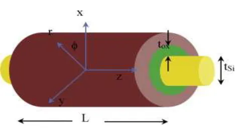
II DEVICE STRUCTURE
706 |
P a g e
We have introduced the 30nm Gate All Around MOSFET for analysis and after depth study of multigate devicesfinally found the results using 2D simulation for the device with change in threshold voltage with various oxide
thickness, silicon thickness and drain to source voltage to explore short channel effects. In the device above radial
direction is assumed along the radius and lateral directions are assumed along z axis of the figure. It has uniform
doping concentration of drain-source keeping channel doping less. The value of silicon film thickness is taken twice
the radius of the cylinder (diameter of cylinder). All the structure junctions are taken as abrupt and biasing condition
at room temperature. This device is the one in which gate oxide is wrapped around channel region and above it gate
electrodes with excellent transconductance and short channel behaviour are embedded. Mobility factor played an
important role in the simulation of the model. In this inversion layer formation effect on threshold voltage and
impact ionization effects are ignored.
Table 1: Parameters used for the simulation
Parameter Symbol Parameter Value
Na Impurity concentration doped in the channel 1016cm-3
Nd Impurity concentration doped in the source and drain 1020cm-3
tsi Thickness of silicon film 10nm
tox Oxide thickness 2nm
L Channel length 30nm
Vacuum Permittivity 8.8*10-12F/m
Silicon Permittivity 11.85*
Oxide Permittivity 3.9*
K Boltzmann constant 1.38*10-23J/K
T Absolute temperature in Kelvin 300K
Silicon Susceptibility 20.75
𝜙m Work Function of metal 4.6*1.6*10-19V
III CALCULATIONS
The potential distribution in the channel region 𝜙(r,z) and is obtained by solving the Poisson equation in a
cylindrical coordinate system:
707 |
P a g e
The flat band voltage of the MOSFET is :Considering channel Length (L) very large, we get the following threshold voltage equation and substituting the
value of flatband voltage we get:
If the equation is replaced by equation of A and B and Vgsby Vth
708 |
P a g e
IV DEVICE SIMULATION
In this section, results are obtained from the theoretical models of the center potential compared with numerical
simulation results. In our results inversion layer formation is not very prominent so neglected.
Fig.2: Threshold voltage with change in channel length at various values of t
siFig.2 shows variation of threshold voltage along the increasing channel length for different silicon film thickness. It
can be seen that Vth increases with decrease in Si film thickness. Vth increases initially but after a certain value
becomes constant with increase in channel length. We have considered standard value upto10nm for silicon film
709 |
P a g e
Fig.3: Threshold voltage with change in channel length at various values of Vds
Fig.3 shows the variation of threshold voltage along the increasing channel length for different drain bias voltage.
The plot shows that the threshold voltage is independent of variation in drain to bias voltage during the turning on of
the device. So no matter how channel length varies, the threshold voltage variation remain same across for all drain
to source voltages.
Fig.4: Threshold voltage with change in channel length at various values of t
oxFig.4 shows the variation of the threshold voltage along the increasing channel length for different gate oxide
710 |
P a g e
control on channel by gate is gradual with increase in gate thickness. In above graph we have assumed standardvalues of gate oxide thickness upto 5nm. So we need to scale the thickness in order to remove the shortcomings in
the device thereby increasing the device efficiency.
V CONCLUSION
The 2D simulations were carried out for various parameters for the centre potential model of CGAA MOSFET. The
graphical values by MATHCAD15 are well matched with the values obtained from SILVACO in the device
simulation of cylindrical Gate All Around MOSFET. The developed model will be useful to advance the device
parameters for the desired performance and for device parameters to be well scaled for use in the circuit.
REFERENCES
1. B. Yu, Y. Yuan, J. Song, and Y. Taur,“ A two dimensional analytical solution for short-channel effects in
nanowire MOSFETs,”IEEETrans.Electron Devices,vol. 56, no. 10, pp. 2357–2362, Oct. 2009
2. K.P.Pradhan, M.R.Kumar, S.K.Mohapatra and P.K.Sahu, “ Analytical modeling of threshold voltage for
cylindrical Gate All Around MOSFET using center potential”, Ains Shams Engg Journal 2015
3. Prashant Mani and Manoj Kumar Pandey, “ Simulation analysis of Narrow width Effect in Nanostructured
Fully Depleted SOI MOSFET”, Procedia computer science,57(2015)637-641
4. Biswajit Ray and Santanu Mahapatra, “Modeling and Analysis of Body Potential of cylindrical Gate All
Around Nanowire Transistor”, IEEE TRANSACTIONS ON ELECTRON DEVICES, VOL. 55, NO. 9,
SEPTEMBER 2008
5. Prashant Mani and Manoj Kumar Pandey, “Analytical solution of 2D Poisson’s equation Using Seperation
of Variable Method for FDSOI MOSFET”, International Journal Of Electronics And Communication
Engineering and Technology,Special Issue (November, 2013), pp. 150-154
6. S.-L. Jang, B.-R. Huang, and J.-J. Ju, “A unified analytical fully depleted and partially depleted SOI
MOSFET model,” IEEE Trans. Electron Devices, vol. 46, pp. 1872–1876, 1998.
7. B. Yu, Y. Yuan, J. Song, and Y. Taur,“ A two dimensional analytical solution for short-channel effects in
nanowire MOSFETs,”IEEE Trans.Electron Devices,vol. 56, no. 10, pp. 2357–2362, Oct. 2009
8. B.A. Rainey, B. M. Fried, M. Ieong, J. Kedzierski, E. J. Nowak,“Demonstration of FinFET CMOS
circuits”, IEEE Dev Res. Conf. Proc., 2002, pp.47-48.
9. Young J, Young W, Park J, Lee J , Park B, Design Optimization of Gate-All-Around (GAA) MOSFETs,
IEEE Transactions on Nanotechnology. 2006;5:186-191
10. Alam K, Abdullah M, Effects of dielectric constant on the performance of a gate all around InAs nanowire
transistor, IEEE Transaction on Nanotechnology. 2012;11:8287.
11. J. Song, B. Yu, Y. Yuan, and Y. Taur, “A review on compact modeling of multiple-gate MOSFETs,” IEEE