GiacomoFedi1,aon behalf of the CMS collaboration 1INFN Sezione di Pisa, Italy
Abstract. The High Luminosity LHC (HL-LHC) will deliver a luminosity of up to 5×1034cm−2s−1, with an average of about 140 overlapping proton-proton collisions
per bunch crossing. These extreme pileup conditions place stringent requirements on the trigger system to be able to cope with the resulting event rates. A key component of the CMS upgrade for HL-LHC is a track trigger system, able to identify tracks with trans-verse momenta above 2 GeV/c already at the first-level trigger. We present here the status of the implementation of a prototype system, based on the combination of Associative Memory custom ASIC and modern Field Programmable Gate Array (FPGA) devices, with the purpose to demonstrate the concept based on state-of-the-art technologies, and to direct the efforts of the necessary R&D toward a final system.
1 Introduction
The increase of the luminosity of the Large Hadron Collider (LHC) to 5×1034cm−2s−1, foreseen in the High Luminosity (HL) upgrade scheduled for 2026, will bring up the number of proton-proton interactions per bunch crossing to an average of about 140 and a maximum of about 175. The corre-sponding higher background will generate an unmanageable increase in the trigger rate of the ATLAS and CMS detectors if their trigger systems will keep the current threshold configurations in order to preserve their physics-analysis capabilities.
One solution could come from the use of high-resolution spatial information from silicon trackers, at the cost of adding a few microseconds of latency and with a large data rate compared to the current L1-trigger. The trajectories of charged particles in CMS are helices since they are bent by the magnetic field generated by a solenoid. When a charged particle passes through the Silicon Tracker, it releases a small amount of energy in the silicon sensors, and the passage of the particle is recorded (“hit”). The CMS tracker for the HL-LHC upgrade will be composed of six (seven) layers of silicon modules in the central (forward) region. Each proton-proton interaction can generate hundreds of charged particles so that the Silicon Tracker generates thousands of hits in each event. Having a multitude of hits, the reconstruction of the trajectory of charged particles in few microseconds becomes challenging.
CMS is exploring three different approaches to tackle this problem: two are based on track re-construction done with Field Programmable Gate Arrays (FPGAs), and one that will be explained in this report which is based on the use of Associative Memory (AM) and FPGAs. The purpose of our R&D activity is to prove that this goal can be achieved by combining pattern recognition based on an
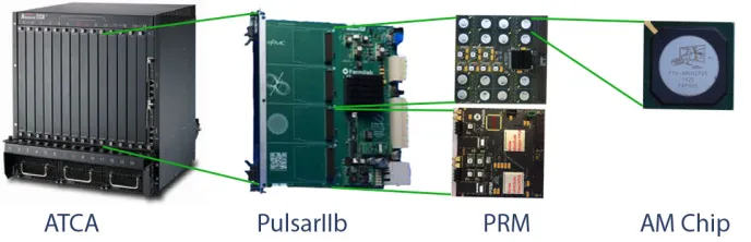
Figure 1. Schematic overview of part of the system. An ATCA shelf accommodates ten PulsarIIb boards and each of them can accommodate two PRMs. Two types of PRM have been developed: one with a full AM chip configuration and one with two Xilinx Ultascale FPGAs and a socket which can accommodate VIPRAM [5] chips.
AM custom chip and computing capabilities available in state-of-the-art FPGA devices. Track finding based on Associative Memories [1] has been successfully used in the CDF experiment [2] and, more recently, is being exploited in the Fast-Track processor [3,4] for the ATLAS Level-2 trigger system.
The CMS outer tracker will be divided in 48 regions inη-φ(pseudo-rapidity and azimuthal angles) called trigger towers. In each trigger tower, the track finding will be performed using data from silicon modules belonging to that region. Each tower will receive an average of 100 hits per layer (the number of layers ranges from 6 to 7 depending on the pseudo-rapidity) in each bunch crossing. We want to build a prototype of the system with the available technology aiming to demonstrate that we will be able to build the full system for the HL phase of the LHC. Such a demonstration will make use of reasonable extrapolations of the technology progress and cost of commercial devices, and the assumption of a strong R&D of the AM chip.
2 Demonstrator system overview
Several boards based on the ATCA technology, the Pulsar IIb boards [6], will collect data from each trigger tower. Each Pulsar IIb board can accommodate two Pattern Recognition Mezzanine (PRM) boards performing pattern recognition and track fitting. Figure1 shows a schematic view of the prototype system.
Each PRM board contains one or two Xilinx FPGAs, implementing data flow management and track fitting, and one or multiple AM devices. Each PRM board receives full resolution data and temporarily stores them in a data buffer. Lower resolution data, called “Super-Strips”, are evaluated and transmitted to the AM chips. The AM chip behaves as a Content Addressable Memory (CAM) and quickly matches the Super-Strips with the pre-loaded patterns. Pre-loaded patterns are based on simulation of the tracks coming from the bunch crossing and of the tracker. Indeed, the tracks are mostly originating in a defined region of the detector, and the curvature of the helical tracks is confined to a certain region of interest (pT>2 GeV/c).
zanine PRM05/06 at INFN and the FNAL PRM. The PRM05 processor is designed to combine the pattern recognition task [8] using the new version of the AM device with the precise track fit-ting [3], performed by the latest generation of FPGA devices, to send out the track information to the higher trigger levels within a latency of a few microseconds. PRM05 has a Xilinx Kintex-7 FPGA (XC7K355T) and 16 AM chips. The board has been developed to accommodate AM05 devices, to test the basic functionality of the serial links, even if the number of patterns stored in each chip is modest (2k patterns).
The current INFN PRM board houses 16 AM custom chips version 05 (AM05). Each chip can store up to 2k patterns, corresponding to a total capacity of 32k patterns per PRM (128k patterns in the AM version 06 chip, “AM06”) to be released in the second quarter of 2016. Each pattern is made of 8 independent 16-bit words, one for each layer. The input data bus distribution from the FPGA to the AM chips uses a first stage of 1-to-2 fan-out buffers to distribute data to the left and right quarters of the card, followed by a second stage of two 1-to-4 fan-out buffers to distribute the data to the 4 AM chips in parallel. The input serial links can sustain a data rate of 2 Gbit/s, while the output data of each AM chip is connected directly to the FPGA using high speed serial lines running at 2.4 Gbit/s.
A second version of the INFN PRM will use a 12 AM chip version 06 where the number of patterns per chip will be increased to 128k patterns for a total of 1.5 million patterns per PRM, which will provide a high efficiency of track reconstruction. The FPGA has the role of distributing the hits to AM chips, collecting the candidate tracks, performing a track fitting on them using a Principal Component Analysis (PCA) [3] and then send out the results to the Global Trigger System. The direct connection between the FPGA and the AM chips has been chosen to eliminate daisy chains and to reduce as much as possible the latency of the Level-1 trigger decision and to integrate all the functionalities in one single board. An external low latency memory is added to increase the data storage capability of the device, in view of possible needs by the different fitting algorithms to be tested.
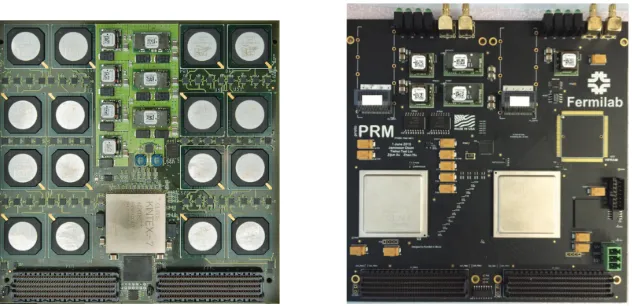
Figure 2.Left: INFN pattern recognition mezzanine board. Right: FNAL pattern recognition mezzanine board.
3 PRM architecture
The PRM board, see Figure2, is a custom 14.9×14.9 cm2printed circuit board housing the following components:
• FMC connectors (2x);
• Xilinx FPGA (1x INFN PRM, 2x FNAL PRM);
• Associative Memory devices (16x INFN PRM, 1x FNAL PRM);
• Power regulators;
• DDRII Pattern Memory (1x);
The two FMC connectors, compliant with the VITA 57.1 standard, are used to interface the PRM to the Pulsar IIb host board. They carry signals and power supply voltages. The host board provides 3.3 V and 12 V, for a maximum available power of 150 W. The power regulator group is used to generate the 1.0 V, 1.2 V, 1.8 V and 2.5 V voltages required by the FPGA, the AM devices and the pattern memory. Regarding the signal lines, 6 bidirectional high-speed serial links (up to 10 Gbit/s), with three links through each FMC connector, are used to send and retrieve data from the PRM with a total bandwidth in input and output up to 120 Gbit/s. Moreover, 68 additional LVDS pair pins are used for the slow configuration and monitoring purposes of the PRM and to provide additional bandwidth for the data transfer. The Xilinx FPGA manages the data flow inside the mezzanine. It receives and temporarily stores the full resolution hit data from the Pulsar IIb board and it evaluates and distributes to the 16 AM chips the lower resolution hit data used in the pattern recognition. Finally, the external pattern memory provides up to 18 Mbit for INFN PRM and up to 36 Mbit for FNAL PRM of memory resources to store a copy of the pattern banks of the AM chips.
4 PRM hardware validation
Both INFN and FNAL PRM boards were validated regarding the electrical circuitry and both showed the expected behavior. The JTAG connection to the FPGA was tested by programming it.
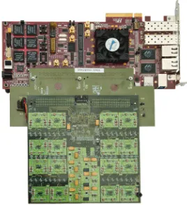
The INFN PRM board was tested using the test stand shown in Figure3. The test stand is com-posed of a PRM board, an adapter card, and an evaluation board. An HTG Virtex-6 evaluation board has been used for the main tests reported in this text. Since the HTG evaluation board has some limitation on the links towards the FMC connectors (only four high speed serial links connected and data rate limited to 6.2 Gbit/s), in order to test the fast serial links of the INFN PRM, an Ultrascale Evaluation board has been also used. The evaluation board is connected to the host PC via Ethernet. It provides power, LVDS parallel connections and high-speed serial connections to the PRM board. The IP-bus protocol is used to access devices in the Virtex-6 and in the PRM FPGAs (e.g.: control and status registers, source FIFOs containing test hits, monitoring FIFOs containing PRM outputs). All the serial links between the FPGAs and to/from the AM chips on the PRM board have been suc-cessfully tested. JTAG connections to the AM chips (4 JTAG chains with 4 AM chips each) have been tested in order to verify the possibility to configure and program the AM chips. The eight input links to each AM chip have been characterized. Pseudo Random Bit Sequences (PRBS) have been used to test the links between the FPGA and the AM chips. The FMC connector links have undergone tests by using a loopback card and the IBERT tool, provided by Xilinx, that allows measuring the Bit Error Ratio (BER) and producing the corresponding eye diagrams. Signal integrity up to 8 Gbit/s has been tested by measuring the BER and the corresponding eye-scans in the receiver links of the PRM and in the receiver links of the Ultrascale board. The BER has been measured using a PRBS-7 sequence. The measured BER was less than 2×10⁻¹⁵in both directions. The power consumption of the board has been measured by powering and configuring the four groups of the AM chips, resulting in a static power consumption of about 40 W. The mezzanine board has been successfully integrated with the Pulsar IIb board in Summer 2015. During these tests the mechanical and electrical compatibility have been verified and both the LVDS and high-speed differential pairs have been fully tested.
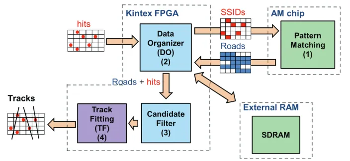
Figure 4.Schematic view of the modules of the track finding algorithm.
5 PRM functionalities
On both INFN and FNAL PRM boards a synthesized HDL code has been developed to implement functionalities needed for the track finding: hit memorization, hit retrieving, and hit fitting. The tracking algorithm implemented in both PRM boards consists of the following sequence of operations, see Figure4:
1. Full resolution hit data received by the host board are decoded and stored in a smart data buffer, called Data Organizer, and coarse resolution hit data, “Super-Strips”, are generated and trans-mitted to the AM chips;
2. AM chips perform pattern recognition on Strip input data and identify sets of Super-Strips matching patterns, called “Road”, that are transmitted back to the FPGA;
3. Roads are used to retrieve the associated Super-Strips from an external pattern memory (cur-rently internal to the FPGA) the associated Super-Strips;
4. Hit data stored in the Data Organizer and belonging to the Super-Strips retrieved from the pattern memory are propagated to the filtering module;
5. The Super-Strips belonging to a road are filtered in such a way that only one candidate track is generated composed of no more than one hit per layer. The set of hits belonging to the candidate track is sent to the track fitter module;
6. The track fitter performs the fitting algorithm using the full resolution data from the Data Orga-nizer to evaluate the track helix parameters and the goodness of the fit.
algorithm showed good performance and limited latency, demonstrating promising results in view of the final test of the system prototype.
Acknowledgments
This work is partially funded by MIUR Italy, under contract 2012Z23ERZ of PRIN 2012 H-TEAM and the People Program (Marie Curie Actions) of the European Union’s Seventh Framework Program FP7/2007-2013/under REA grant agreement no. 317446 INFIERI “INtelligent Fast Interconnected and Efficient Devices for Frontier Exploitation in Research and Industry”.
References
[1] M. Dell’Orso, L. Ristori, Nucl. Inst. & Meth. A278, 436 (1989)
[2] J.A. Adelman et al. (CDF collaboration), Nucl. Inst. & Meth. A572, 361 (2007)
[3] C. Gentsos, F. Crescioli, P. Giannetti, D. Magalotti, S. Nikolaidis, PoSTIPP2014, 209 (2014) [4] F. Alberti et al., JINST8, C01040 (2013)
[5] T. Liu, G. Deptuch, J. Hoff, S. Jindariani, S. Joshi, J. Olsen, N. Tran, M. Trimpl, JINST10, C02029 (2015)
[6] J. Olsen, T. Liu, Y. Okumura, JINST9, C01041 (2014) [7] M. Jeitler et al., JINST2, P01006 (2007)