Performance Study of Swastika Shaped Microstrip Patch
Antenna loaded with Meta-material Layer
Shahriar Rahman
American International University Bangladesh (AIUB)
Banani, Dhaka
M Tanseer Ali
, PhD Assistant Professor American International University-Bangladesh (AIUB)Banani, Dhaka
ABSTRACT
Now-a-days wireless communication has made the world a smaller than it used to be a couple of decades ago. With the evolving technologies emerging, a continuous and seamless connectivity with the artificial planetary objects such as Satellite and ground station has become a demand of time. Hence researchers are relentlessly working on to overcome the challenge of integrating a budget-friendly yet miniature in shape and multimode supporting antenna in wireless devices. Microstrip Patch Antenna, a technology invented in the 70s, can easily accommodate the entire requirement. But there are some trade-off in terms of performance and design. In this particular paper we analyzed the performance of a slotted Swastika Shaped microstrip Patch antenna with meta-material layer. The probe feeding technique and design structure provides the antenna to operate in five different frequencies. The antenna resonates at 9.11 GHz in X band and 12.56 GHz, 13.82 GHz, 14.71 GHz and 15.50 GHz in X band with return loss of -17.84 dB, -13.86 dB, -13.52 dB, -20.4 dB and -15.9 dB respectively of proposed antenna have been examined and discussed.
Keywords
Microstrip Patch Antenna (MPA), Rectangular Microstrip Patch Antenna (RMPA), Electromagnetic (EM), Meta-material
1.
INTRODUCTION
James Clerk Maxwell, a Scottish scientist, developed the proper and one of the most modern theories of electromagnetic wave properties. The equation that he developed during his research on this field is considered as one of the most insightful work that actually helped to develop practical applications of wireless communication. There are countless ranges of frequency bands for various communication systems that are currently available in this modern age. And these frequencies have been divided into quite a few segments depending on their purpose and application. These particular segments are referred in scientific nomenclature as ‘bands’. Hence integrating multiple bands in a given wireless communication device would mean one single device can be used for varied scales of communication. In order to make multiband operation possible, the antenna of the wireless communication device has to be able to transmit and receive multiple frequencies. There are different types of antennas [1 & 2] out of which Microstrip Patch Antenna (MPA) is the most widely used around the globe. The basic structure of the antenna is built using conducting patch of any non-planar or even planar geometry in a side along with the dielectric substrate. On the other side is the ground plane [3]. This structure has high
level of multilateral leads for its planar profile. Moreover it has the capacity to operate in microwave frequency range, the manufacturing process is economic and mostly the construction in integrated circuit is simpler compared to conventional antenna. As a result of these advantages and some added perks i.e. light weight, low volume, lower fabrication costing etc; these antennas can be mass produced [4-6]. But MPAs are not full of benefits; there are some disadvantages as well. Low efficiency, single frequency operation and narrow impendence bandwidth etc are the some of the most pressing concerns in MPA.
Recently many researchers from various industries and universities who are working on MPAs have invented several multiband antenna techniques, amongst them are loading the patch with shorting pins [7-9], using two feeding ports [10], loading slits [11], using stacked patches [12-15], PIN diodes, switches and varactor diodes. One of the most important shortcoming of the design is the requirement for controlling turn ON/OFF switch for reconfigurable frequency operations [16-18] using slots in the patch [19 & 20]. To avoid these shortcoming some changes can be brought in the structure. For example: Rectangular Slot, Square Slot, V-Slot, T-Slot, U-Slot and countless other shapes are generally integrated into the patch of antenna. So, in order to get better impedance bandwidth a number of techniques may be applied such as increasing the substrate thickness [21], covering the patch by additional dielectric layers [22 & 23], introducing parasitic element either in coplanar or in multilayer configuration [24], and performing slots in radiator patch [25]. Out of all, slotting is considered as one of the best approach. The slots help to perturb the surface current path on the patch that generates local inductive effect which is responsible for multiband operation. So far compared to all the approach, slot technique is by far the most promising one because it can provide excellent bandwidth improvement and maintain a single-layer radiating structure with multiband feature. Beside adding slotted Meta-material layer [27] improves the gain, directivity of an antenna. Studying the above stated literature we were motivated to design an MPA which operates in multiband application.
2.
ANTENNA DESIGN
The antenna configuration has been made on the conventional Rectangular Microstrip Patch Antenna (RMPA). The whole design of the proposed antenna is developed in IE3D EM simulator software using low cost FR4 substrate material of
thickness h=1.6 mm and permittivity
r= 4.31. The antennastructure of proposed antenna. The initial parameters are determined from the following equation [26].
1 2 2 r r f o W
(1) 2 1 12 1 2 1 2 1 W h r r eff
(2)
8
.
0
258
.
0
264
.
0
3
.
0
421
.
0
h
W
h
W
h
L
eff eff
(3) L f L o o eff r 2 2 1
(4)Here W is the width of the patch, vo is the speed of light in a
vacuum, εr is the dielectric constant of the substrate, fr is the
target frequency, εeff is the effective dielectric constant of the
[image:2.595.318.545.72.246.2]substrate, ΔL represents the extension in length caused by the fringing effect, h is the thickness of the substrate and L is the length of the patch.
Fig 1a: Design of Proposed antenna
[image:2.595.55.246.98.288.2]Fig 1b: Design of the SRRs of the proposed antenna
Fig 2: Radiating patch of proposed antenna
[image:2.595.56.281.370.685.2]The RMPA and proposed antenna both have patch and ground plane dimension of (L x W) 25mm x 11mm and (L1xL1) 23.2mm x 23.2 mm respectively. For proposed antenna four modified slots have been cut off. These are different from the rectangular patch. By interrupting the surface current on the patch a local inductive effect is generated. This effect responsible for the multiband attribute of the antenna. Here in this particular design the slots are trimmed off in precise manner so that 90, 180, 270 and 0 degrees phase shift of capital alphabet “E” shape copper plate can be plot into the slots without any attachment to the main patch. In Figure 1b slots dimensions are illustrated through Table 1.It can be noticed that another extra substrate layer has been fastened on the main slotted patch with same dielectric constant of 4.31.This is as the substrate of proposed antenna in between patch and ground plane, shown in Figure 2. It has been done to increase the bandwidth of the overall antenna and improve other antenna characteristics.
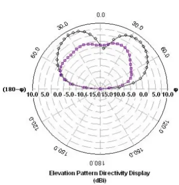
Table 1. Dimension of Proposed Antenna
Parameters Dimensions (mm)
L1 23.2
L2 15.0
L3 4.0
L4 3.0
L5 5.0
L6 1.0
la 6.0
lb 0.4
wa 7.0
wb 2.0
wc 0.7
lc 4.5
wd 0.4
we 1.0
wf 5.5
Feed point
[image:2.595.307.548.474.753.2]3.
SIMULATION AND RESULT
[image:3.595.311.549.72.241.2] [image:3.595.57.289.237.379.2]IE3D, the software used for this simulation, is an integrated full wave EM simulator which has optimization package for analysis and design of 3D and planar microwave circuits. In antenna designing and simulation the result that it provides is accurate and precise. Here, the dimensions mentioned in the table for the proposed antenna are transferred to the software for analysis. Figure 3 represent the RMPA performance in terms of return loss and frequencies. The conventional RMPA resonates at 11.26 GHz and 13.37 GHz with return loss of -18.29 dB and -20.27 dB respectively. The distinct feeding position and technique enables the RMPA to operate in X and Ku band. It can be noted that the bandwidth of the operating frequencies is after -10 dB critically which are 163 MHz and 250 MHz respectively.
Fig 3: Reflection coefficient of RMPA
Figure 4 illustrates the reflection coefficient of the proposed antenna. It has been observed that the antenna operates in six different frequencies under X and Ku band. The resonant frequencies are 9.11 GHz, 12.56 GHz, 13.8 GHz, 14.71 GHz, 15.5 GHz with return loss 17.84dB, 13.86dB, 14dB, -20.4dB and -15.9dB respectively. The bandwidth of the operating frequencies are 266 MHz for first and second, 488 MHz for third, 1400 MHz for fourth and fifth and 1060 MHz for sixth resonant frequency.
Fig 5: Reflection coefficient of Proposed Antenna
Comparing from the figure 3 and figure 4 it is cleared that proposed antenna has better performance than RMPA. Proposed antenna has six resonant frequencies and the bandwidth covers 6.65% of X and 49% of Ku band, where as RMPA have only one proper resonant frequency and the bandwidth covers 4% of X and 6% of Ku band. The extra layer of substrate on the top of patch enhances the performance of proposed antenna
Antenna
Parameters RMPA
Proposed Antenna X
Band Ku Band
Resonant Frequencies
(GHz) 12.7 9.11 12.56 13.8 14.71 15.5
Return loss
(dB) -17
-17.84
-13.86 -14 -20.4 -15.9
Bandwidth
(MHz) 170 266 488 1400 1060
Directivity
(dBi) 4.2 8.732 8.88 8.8 9.03 8.6
Gain (dBi) 8.5 2.4 4.8 6.72 7.704 5.134
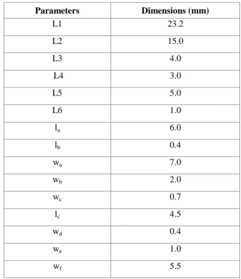
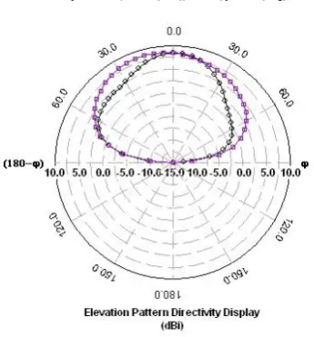
[image:3.595.337.510.339.525.2]Figure 5-9 shows 2D directional radiation pattern of proposed antenna. Higher directivity implies a more focused antenna. At operating frequencies the directivities are 7.44 dBi, 6.67 dBi, 7.44 dBi, 8.02 dBi, 6.66 dBi, and 7.01 dBi respectively. The figure shown below for the elevation pattern from φ = 0 and φ = 90 degrees.
[image:3.595.55.288.501.628.2]Fig 5: Directivity at 9.11GHz of Proposed Antenna
[image:3.595.334.509.560.747.2]Fig 7: Directivity at 13.82 GHz of Proposed Antenna
Fig 8: Directivity at 14.71GHz of Proposed Antenna
Fig 9: Directivity at 15.5GHz of Proposed Antenna
4.
CONCLUSION
Due to extensive use in handheld devices, Micro strip antennas have become a fast emergent area of investigation. The potentiality of this particular genre of antenna is infinite; thanks to the light weight and compact structure and easy fabrication facility. In this paper an innovative design with Swastika Shaped Microstrip Patch Antenna loaded with Meta-material Layer was investigated using is an integrated full wave EM simulator. It was found that the feeding position and the unique technique have provided the antenna to operate in X (8-12 GHz) and Ku (12-18GHz) band. It was also concluded that the slots help to agitate the surface current path on the patch that generates local inductive effect which is responsible for multiband operation. We find this design very helpful for inter-galaxy and inter-satellite communication.
5.
REFERENCES
[1] Puente, Borja, Navarro, and Romeu, “An Iterative Model for Fractal Antennas: Application to the Sierpinski Gasket Antenna”, IEEE Transactions on Antennas and Propagation, Vol. 48, No. 5, pp 713-719, May 2000.
[2] Z.D. Liu, P.S. Hall, and D. Wake, Dual-frequency planar inverted-F antenna, IEEE Trans Antennas Propagat 45 (1997), 1451–1458.
[3] David M. Pozar, “Microstrip Antennas”, Proceedings of IEEE, Vol. 80, No. 1, January 1992.
[4] Ramesh, G., B. Prakash, B. Inder, and I. Apisak, Microstrip Antenna Design Handbook, Artech House, USA, 2001.
[5] James, J. R. and Hall, P. S., “Handbook of Microstrip Antennas” (Peter Peregrinus), Vol. 2, 1989
[6] Constantine A. Balanis, “Antenna Theory: Analysis and Design”, John Wiley & Sons, 3rd Edition, 2005
[7] C. L. Tang, H. T. Chen, and K. L. Wong, “Small circular Microstrip antenna with dual-frequency operation,” IEEE Electron. Lett., vol.33, no. 13, pp. 1112–1113, Jun. 1997.
[8] K. L. Wong and W. S. Chen, “Compact microstrip antenna with dual frequency operation,” IEEE Electron. Lett., vol. 33, no. 8, pp. 646–647, Apr. 1997.
[9] S. C. Pan and K. L. Wand, “Dual frequency triangular Microstrip antenna with shorting pin,” IEEE Trans. Antennas Propag., vol. 45, pp. 1889–1891, Dec. 1997.
[10]J. F. Zurcher, A. Skrivervik, O. Staub, and S. Vaccaro, “A compact dual-port dual-frequency printed antenna with high decoupling,” Microw Opt. Technol. Lett., vol. 19, pp. 131–137, Oct. 1998.
[11]Indra Surjati, “Dual Frequency Operation Triangular Microstrip Antenna Using A Pair Of Slit”, 2005 Asia-Pacific Conference on Communications, Perth, Western Australia, pp. 125-127, 3 – 5, October 2005.
[12]L. Zaid, G. Kossiavas, J. Y. Dauvignac, J. Cazajous, and A. Papiemik, “Dual-frequency and broadband antennas with stacked quarter wavelength elements,” IEEE Trans. Antennas Propag., vol. 47, no. 4, pp. 654–660, Apr. 1999.
[image:4.595.72.252.555.741.2][14]F. Croq and D. M. Pozar, “Multi-frequency operation on Microstrip antennas using aperture coupled parallel resonators,” IEEE Trans. Antennas Propag., vol. 40, no. 11, pp. 1367–1374, Nov. 1992.
[15]J. Wang, R. Fralich, C. Wu, and J. Litva, “Multifunctional aperture coupled stack patch antenna,” IEEE Electron. Lett., vol. 26, no. 25, pp. 2067–2068, Dec. 1990.
[16]D. Peroulis, K. Sarabandi and L. B. P. Katehi. 2005. Design of reconfigurable slot antennas. IEEE Trans. Antennas Propag., vol. 53, no.7, pp. 645-654.
[17]H. Okabe and K. Takei. 2001. Tunable antenna system for 1.9 GHz PCS handsets. IEEE Antennas Propag. Int. Symp., vol. 1, pp. 166- 169.
[18]F. Yang and Y. R. Samii. 2002. A reconfigurable patch antenna using switchable slots for circular polarization diversity. IEEE Micro. Wireless Comp. Lett., vol. 12, no. 3, pp. 96-98.
[19]S. Maci, G. B. Gentili, P. Piazzesi, and C. Salvador, “Dual band slot loaded patch antenna,” Proc. Inst. Elect. Eng. Microw. Antennas Propag., vol. 142, pp. 225–232, Jun. 1995.
[20]B. F.Wang and Y. T. Lo, “Microstrip antennas for dual-frequency operation,” IEEE Trans. Antennas Propag., vol. 32, pp. 938–943, Sep. 1984.
[21]Yang Fan, Y. Rahmat-Samii, "Microstrip antennas integrated with electromagnetic band-gap (EBG) structures: a low mutual coupling design for array
applications" IEEE Transactions on Antennas and Propagation, Volume:51 , Issue: 10, pp: 2936-2946, Oct.
[22]N. G. Alexopoulos and D. R. Jackson, “Fundamental superstrate (cover) effects on printed circuit antennas,” IEEE Trans. Antennas Propag., vol. AP-32, pp. 807–816, Aug. 1984.
[23]Kim, J., H. Kim, and K. Chun, \Performance enhancements of a microstrip antenna with multiple layer substrates," International Symposium on Signals, Systems and Electronics 2007 (ISSSE '07), 319{322, 2007.
[24]K.F. Lee and R.Q Lee, “Microstrip subarray with coplanar and stacked parasitic elements”, Electronics Letters, Volume: 26, Issue: 10, 1 May 1990.Transactions on Antennas and Propagation, Volume: 51 , Issue: 10, pp: 2936-2946, Oct. 2003.
[25]X.L. Bao, M.J. Ammann, "Small patch/slot antenna with 53% input impedance bandwidth", Electronics Letters, Volume 43, Issue 3, pp. 146 – 148, Feb 2007.
[26]Razin Ahmed, Md. Fokrul Islam, “E shaped Microstrip Patch Antenna for Ku band” Published in International Journal of Computer Applications Volume 80, No.6, October 2013