Area-Delay Estimation by Concurrent Optimization of
FPGA Architecture Parameters using Geometric
Programming
Y. Pandurangaiah
Head of the Department(ECE)Vardhaman College of Engg Hyderabad, India
J. Venkat Reddy
StudentVardhaman College of Engg Hyderabad, India
G. Kalyan Chakravarthy
Assistant Professor Vardhaman College of EnggHyderabad, India
ABSTRACT
This paper presents the application of geometric programming for combined high-level and low-level architecture parameter exploration. This paper builds an geometric programming framework for reconfigurable architectures, and presents a full delay and area model of an FPGA. This optimization allows high-level architectural parameter selection and the transistor sizing to be done concurrently. The transistor values are derived using 45nm predictive technology model. CVX framework for MATLAB is used to run the geometric programming framework. The area and critical path delay are determined for given cost function by single-stage and multi-stage approach.
General Terms
CVX framework, Field Programmable Gate Arrays (FPGAs), Predictive Technology Model (PTM)
Keywords
Geometric Programming, Reconfigurable architectures
1.
INTRODUCTION
In recent years, a considerable evolution in the architecture of FPGAs and this enhancements in the architectures, results in a expensive and time consuming experiments. Commercial FPGAs of every generation contains refined or new routing, memory, logic and embedded block structures. New or existing CAD tools are used by FPGA architects to map benchmark circuits to the architectures [3], [5]. Recent work, has suggested that the analytical techniques serve as the supplement to the experimental approach, in which the FPGA architectures are constructed using a model of relatively simple equations. Using this technique, the FPGA architect can investigate a much wider range of architectures.
The advantage of analytical approach is that the values for many architectural parameters can be optimized concurrently, which is different from experimental approach, in which typically one parameter is swept at a time. In [1], the simultaneous optimization of several parameters of routing structures of an FPGA by creating analytical equations and the impact of these parameters on the area of an FPGA is been shown, and a Geometric Programming (GP) framework is used to determine the values for these parameters.
In this paper, the simultaneous optimization of transistor sizing and architecture is done, which allows us in optimizing the both area and critical path delay (speed) of the FPGA. The work can be summarized as follows:
A framework allowing, concurrent optimization of both low-level (transistor sizing) and high-level (architectural) parameters.
Using geometric programming an area-delay model of an FPGA fabric is formulated.
Concurrent optimization of low-level and high-level parameters will lead to a significantly different architectural conclusions compared to a traditional flow. Particularly, cluster size should be increased rather than decrease leading to delay improvements as delay becomes more important than area.
In [7], the general formulation for optimization of an electrical design based on an iteration process, involving successive routing and placement of circuits onto FPGA architectures is presented. In this work, the iterative refinement is removed, building an FPGA modeling technique and using a geometric program, a step of transistor sizing concurrently to a number of architectural parameters.
A geometric program is a constrained optimization problem of the following form:
Minimize : f0(x)
Subject to : gi(x) = 1, for i = 1,2, ..., l
where x is positive n-vector of real values, and functions fi
and gi have special mathematical forms, known as
posynomials and monomials, respectively. A monomial is a function
g(x) = cx1a1x2a2 . . . xnan
where the coefficient c must be positive. As an example, in this paper a monomial cost function (Ttotal)z(Atotal)z is used,
where Ttotal and Atotal represent the variables delay and area
respectively and z is a constant. Geometric programming is used extensively for circuit design problems, which include wire sizing, transistor sizing and robust design. Use [6] for extensive review of geometric programming in the context of circuit design.
2.
ARCHITECTURE FRAMEWORK
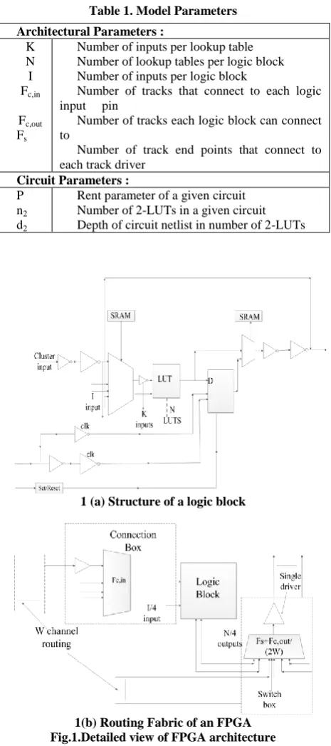
Table 1. Model Parameters
1 (a) Structure of a logic block
1(b) Routing Fabric of an FPGA Fig.1.Detailed view of FPGA architecture
Figure 1(b) shows the routing architecture, which consists of switch boxes and connection boxes. Three parameters are used to describe the routing blocks in the architecture :
Fc,in : number of tracks that connect to each logic
block input,
Fc,out : number of tracks that each logic block output
can connect and
Fs : number of track end points that connect to each
channel driver.
3.
DELAY MODEL
It has been shown previously that geometric programming is capable of optimizing the transistor sizing for delay [15]. Here this type of delay optimization technique is employed to model the combination of pass transistor structures and CMOS present in FPGA devices. The delay of a critical signal path through a circuit implemented on FPGA is considered. The critical path will pass through CLBs, CLB feedback paths, LUTs, connection boxes and switch boxes. The formula in (1) is used, where each term is described below.
Ttotal = Treg to OMUX + DiTLUT F/B path + (Dk - 1)TLUT delay
+ DcTO/P CB delay + DcDrTSB delay
+ DcTI/P CB delay + DcTinput MUX delay
+TLUT to reg delay. (1)
Dc represents the number of CLBs through which the critical
path travels. Dk represents depth of the netlist when
implemented in K-input LUTs.
Di = Dk - Dc represents the number of the internal feedback
connections through which critical path traverses. Dr
represents number of switch boxes through which the each external connection on the critical path propagates. To estimate the net list depths Dc, Dk and Di the methods are
employed from [19].
Each transistor in the circuit can also be represented as an RC network as shown in the figure 2. The capacitance and resistances values can be derived from the SPICE models of MOSFET devices. Here the values are derived using the 45nm predictive technology model [14]. Each resistance value for a transistor in architecture takes the form (2) and capacitance of form (3) or (4). RC, CD and CG represent the channel
resistance, diffusion capacitance and gate capacitance of a transistor respectively. Si represents the width of transistor
assuming all the transistors have minimum length. Rnom and
Cnom,x nominal values are dependent on the process
[image:2.595.317.548.491.671.2]technology, the type of transistor and in case of capacitance, whether it is nominal diffusion or gate capacitance.
Fig. 2. RC delay model for a MOSFET
RC = Rnom/Si (2)
CG = Cnom,GSi (3)
CD = Cnom,DSi (4)
The delays through each of the paths (1) are evaluated, by
Architectural Parameters :
K N I Fc,in
Fc,out
Fs
Number of inputs per lookup table Number of lookup tables per logic block Number of inputs per logic block
Number of tracks that connect to each logic input pin
Number of tracks each logic block can connect to
Number of track end points that connect to each track driver
Circuit Parameters :
P n2
d2
segment is the sum of the resistance along the path multiplied by capacitance of that segment.
T
=
C R
i source to Ci
elmore
paths i source to sink
(5)
The expression of the total delay can be derived by breaking down the delay terms Tx in (1) into its constituent paths. Each
path begins at VDD or GND and ends at a transistor gate input, which leads to a number of paths as given in figure 3(a-j).
The delay Treg to OMUX corresponds to the delay from the
register producing critical signal path over the MUX selecting whether the LUT output is being registered or not, and over the two-level buffer as given in Figure 3(c).
The delay TLUT F/B path corresponds to the delay from the BLE
output buffer over the pass transistor based MUX on the LUT input to its buffer, as given in figure 3 (b).
The delay TLUT delay corresponds to the delay from the LUT
driver over all the levels of the multiplexer implementing the LUT, the 2:1 MUX and to the LUT output driver. This delay is the sum of the paths given in Figure 3(h) and 3(e).
The delay TO/P CB delay corresponds to the delay from the BLE
output buffer over the switch box multiplier to its first inverting buffer, as given in Figure 3(b). In this case the Elmore delay is through the path to the switch box driver.
The delay TSB delay corresponds to the routing path signal
between switchboxes. This represents sum of the driver delay and delay over the two level switchbox multiplier, as given in Figure 3(a) and 4(i).
The delay Tinput MUX delay corresponds to the delay from the
connection box output driver over the LUT input select multiplexer to the LUT input driver.
The delay TI/P CB delay corresponds to the path over the
switchbox to the connection box, where the routed signal is consumed. This is the sum of the delay over the connection box, the driver delay and over the two inverting drivers in the connection box. These are given in Figure 3(a), 3(i) and 3(j) respectively.
Finally, the delay TLUT to reg delay corresponds to the delay over
the multiplexer implementing the LUT to the register input where the critical path terminates, as in Figure 3(f).
Since each driving gate has two paths to consider: the charge and discharge path from the driving gate, the terms representing delay are given as inequalities. As an example, the inequality for the charge path through the nMOS transistor which corresponds to the delay TO/P CB delay as given in (6), as
in the Figure 3(b).
3 (a)
3(b)
3(c)
[image:3.595.333.520.64.705.2]3(e)
3 (f)
3(g)
3(h)
3(i)
[image:4.595.92.547.83.776.2]
3(j)
Fig. 3. RC delay models for circuit path
O/P CB delay C,n,LOdrv2 D,n,LOdrv2
D,mux c,out D,SB _ mux
C,LOdrv2 C,SB _ mux D,SB_mux
C,LOdrv2 C,SB _ mux
D,SB
T
R
(C
NKC
F
C
)
(R
R
)2 C
(R
2 R
)
(C
_ mux
C
G,SB _ driver)
(6)
4.
AREA MODEL
An area model of an FPGA routing fabric alone was first presented in [1], and is summarized in section 4.2. In this work the model is extended to deal with variable buffer sizing and include both the routing and logic architecture. The area model is based on minimum width transistor sizing model employed in [5].
To evaluate how much logic area is consumed, use
2
c c
N
[ n ]
, where nc is the number CLBs and estimated
using the formula in [4]. The total area of an FPGA, Atotal
corresponds to the sum of the logic area Al and routing area
Ar, as in (7).
total l r
A
A
A
(7)
4.1
Logic Block Area
The area of the logic block is sum of the area dedicated to the following: the LUT input select multiplexer; the LUT, 2:1 multiplexer register and output buffer combination; the clock buffer and the set/reset logic. The clock buffer sizing and set/reset logic are assumed to be constant irrespective of the logic block architecture, the values are taken from [5]. Similarly, the size of the register size on the LUT output is assumed to be constant.
The LUT area is composed of pass transistors multiplexer cells, SRAM cells and internal drivers. The pass transistors size in the multiplexer (Sn,LM) is assumed to be equivalent.
Similarly, the input buffer scheme is assumed to have the same size transistors. Bli represents the sum of these buffer
corresponds to the size of each two pass transistors implementing 2:1 multiplexer and SSR corresponds to the one
bit configuration memory required.
A
21mux
S
SR
2S
n,21mux (9)The sum of the transistor areas for the two inverters implementing the driver gives the output buffer combination. The area consumed by these combination of inverters is given by (10).
n,LOdrv1 p,LOdrv1 n,LOdrv2 p,LOdrv2
B
lo
S
S
S
S
(10)
where Sn,LOdrv* and Sp,LOdrv* represents the size of each nMOS
and pMOS transistors respectively in a CMOS inverter.
An expression for the approximation of multiplexer area is given by (11) and (12). The Sn corresponds to the size of pass
transistor and E corresponds to the number of inputs.
mux n SR
E
A
S (E [ E ])
S
([
] [ E ])
E
(11)
n SR
S (E
E) 2S
E
(12)
Each input select multiplexer is fully connected; every output feedback path and every input from the connection box can reach any LUT input, which leads to the expression in (13), which gives the area devoted to each of these multiplexers. Sn,ISmux corresponds to the size of the pass transistors
implementing the input select multiplexer. Since there are I+N inputs to the multiplexer, in (14) EIS,tree corresponds to the
number of pass transistors in the multiplexer tree and in (15) EIS,tree corresponds to the number of SRAM bits.
ISmux IS,tree n,ISmux IS,RAM SR
A
E
S
E
S
(13)
IS,tree
E
N
I [ N
I]
(14)
IS,RAM
E
[ N
I] [ N
I]
(15)
Combining the above constituent parts of the logic block leads to an expression in (16). The total area of the FPGA fabric is given in (17).
LB LUT reg 21mux ISmux clkB rst
A
NA
NA
NA
KNA
NB
A
A
lo
(16)
c LB
A
l
N A
(17)
4.2
Routing Area
The amount of silicon area devoted to the routing fabric to consist of all the connection box and switch box multiplexers, in addition to their configuration memories and output buffers. Thus, the routing area will depend on the size of the multiplexers used to connect the signals to and from the logic
blocks and I/O pins, the transistor sizing, the channel width and the size of the grid of logic cells.
The estimation of multiplexer sizes in the connection and switch boxes is based on the observation that the expression for the area of two level multiplexer in (11) can be approximated as given in (12). The size of these multiplexers will depend on the channel width of the device.
The model developed in [2] is used to estimate the channel width. The model for architectures with the wires that span one logic block is shown in (18), where the minimum channel width Wmin is described by (19), and β, αin, αout and pf are
empirical constants. In (19), λ corresponds to the average
number of inputs used on each logic block and
R
corresponds to the average point-to-point wire length. The methods given in [9] are used to calculate the value of point-to-point wire-length for different logic parameters.out in
min min min min
s c,in c,out
W
W
W
1
W
W
(
)(
)
(
)
F
F
F
(18) min fR
W
p
2
(19)In routing fabric there are two types of multiplexers: connection box multiplexers and switch box multiplexers. Using the approximation of (12) gives the expression of multiplexer area for the connection box as given in (20) and
(21) gives the approximation of switchbox area.
c,in c,in F F W
corresponds to the number of tracks that connect to the each
logic block input and
c,out c,out F F W
corresponds to the proportion of routing tracks that the each logic block output connects to. Combining the above models lead to (22) for the routing area.
cb n,cb c,in c,in SR c,in
S
S
(WF
WF ) 2S
WF
(20)
sb,m n,sb c,out s c,out s
SR c,out s
N
N
S
S
F
F
F
F
2
2
N
2S
F
F
2
(21)r c cb cb io c cb,io cb,io s,m sb,m sb,m s,e sb,e sb,e
A
IN (S
B ) 4 I
N (S
B
)
W(S
B
) 6 N
W(S
B
)
(22)
5.
GEOMETRIC PROGRAMMING
FORMULATION
z
0.5
. The exponent weight must be constant for each runof the GP.
z 1 z
total total
min : T
A
(23)
The model presented in before section is not in a form that is conformable to GP. The GP representation of the routing architecture model was given in [1], here the focus is on presenting the logic area constraints in the correct form.
The sum of nMOS and pMOS transistors for each inverting stage gives the area of its each respective buffer in the FPGA
, for example Blo in (10). The expressions (24) and (25)
gives the transformation into posynomial form for buffer area,
where
B
xcorresponds to the area of the buffer x.x n p
all inverters in x
B
S
S
(24)
1 1
n x p x
all inverters in x
S B
S B
1
(25)
The expressions (26)-(30) gives the area constraints in a standard form GP representation. The sum of logic area and routing area in (7) maps directly to the inequality constraint in (31), which gives an example, how the model maps to the constraints.
K 1 1 K 1 1
SR lut lut n,LM lut
2 S A
KB A
li
2
2 S
A
1
(26)
1 1
SR 21mux n,21mux SR 21mux
S A
2S
S A
1
(27)
1 1
IS,tree n,ISmux ISmux IS,RAM SR ISmux
E
S
A
E
S A
1
(28)
1 1 1
LUT LB reg LB 21mux LB
1 1
ISmux LB LB
1 1
clkB LB rst LB
NA
A
NA A
NA
A
KNA
A
NB A
A
A
A A
1
lo (29) 1 c LBN A A
l
1
(30)
1 1
total total r
A
A
l
A
A
1
(31)
The mapping of delay constraints is straightforward, as they take the posynomial form. The expressions (32)-(41) gives an example how delay constraints are represented in GP. The example shows the delay and the related constraints between the inverters used in the switch box buffer. The expressions in (32) and (33) represent the charge/discharge path of first inverter through pMOS and nMOS transistors respectively,
where TSB inv1 inv 2 corresponds to the variable
C
to the nominal values for a minimum gate length transistor in given technology.
1
SB inv1inv 2 C,n ,SB _ inv1 D,n ,SB _ inv1 1
SB inv1inv 2 C,n ,SB _ inv1 G ,SB _ inv 2
T
R
C
T
R
C
1
(32) 1SB inv1inv 2 C,p,SB _ inv1 D,n ,SB _ inv1 1
SB inv1inv 2 C,n ,SB _ inv1 G ,SB _ inv 2
T
R
C
T
R
C
1
(33) 1G ,SB_inv 2 G ,p,SB _ inv 2 1
G ,SB _ inv 2 G ,n ,SB _ inv 2
C
C
C
C
1
(34) 1 1nom,nMOS C,n,SB_ inv1 n,SB_inv1
R
R
S
1
(35)
1 1
nom,pMOS C,p,SB _ inv1 p,SB _ inv1
R
R
S
1
(36) 1
nom,D,nMOS D,n,SB_ inv1 n,SB_ inv1
C
C
S
1
(37) 1
nom,D,pMOS D,p,SB_ inv1 p,SB_ inv1
C
C
S
1
(38) 1
nom,G,nMOS G,n,SB_ inv2 n,SB_ inv2
C
C
S
1
(39)
1
nom,G,pMOS G,p,SB_ inv2 p,SB_ inv2
C
C
S
1
(40)
1 TECH n,SB_ inv1
S
S
1
(41)
The expression in (41) used to ensure that the transistor size does not violate the smallest feature size possible in the
process technology, where
S
TECH corresponds to the constantrepresenting the minimum feature size. The final constraints must be applied to all transistors in the GP.
The Geometric program takes approximately 43 seconds to run on a Intel Dual Core i5-2450M 2.5GHZ running windows 7. This is for each K and N logic parameters sweep.
6.
RESULTS
To demonstrate the power of Geometric Programming framework, the framework is run using CVX framework in MATLAB [11]. Two different flows using Geometric Programming framework are modeled, to demonstrate the impact of concurrently optimizing the low-level and high-level parameters.
4 (a)
In the second experimental approach, each of K, N, Fc,in and
Fc,out is successively chosen. This experimental flow is as
shown in Figure 4(b). The sweep across
K
2 7
, will determine the best LUT for an randomly chosen value of N, Fc,in and Fc,out. Then K is fixed and then sweep across the CLBsize
N
2 12
. Similarly, the routing flexibility parameters are chosen from a sweep of different values.
4(b)
Fig.4.The two flows used in the experiment
Figure.5 (a). Area of each approach
Figure.5(b) Critical path delay of each approach
During the exploration the exponent parameter z was varied to check how each approach performs depending on the weight of cost function. Figure 5(a) shows the area in minimum width transistors when varying the exponent z in the objective
function of
z 1 z total total
T
A
and Figure 5(b) shows the critical path delay of each architecture. In single stage approach the delay improves when the cost function is weighted towards delay as objective. The multi-stage heuristic performs worse for both metrics - around 1% in area and 6% in delay compared to the best architecture.
The geometric programming approach can be rewarded in terms of run time. The geometric program framework takes approximately 40 seconds to solve, whereas, VPR tool takes approximately 5 minutes to run an architecture file.
7.
CONCLUSION
This paper presents the use of Geometric Programming for fast and early stage exploration of configurable architectures. This approach allows the concurrent optimization of high-level and low-high-level architecture parameters, and shows that it is possible to gain in performance. In this experiment, the transistor values are derived using 45nm predictive technology model (PTM). The graphs are plotted for area and delay of the architectures for both single and multi-stage approach by varying the exponent z in the objective function
z 1 z total total
T
A
. 0 0.5 1 1.5 2 2.5
0 0.1 0.2 0.3 0.4 0.5 0.6 0.7 0.8 0.9 1 First Experiment approach
Second Experiment approach
0 1 2 3 4 5
0 0.1 0.2 0.3 0.4 0.5 0.6 0.7 0.8 0.9 1
First Experiment approach Second Experiment approach
C
ri
ti
cal
Pa
th D
el
ay
(ns
)
In future work, spice is used to extract accurate delay information and wire delay model can also be included to improve the accuracy of the modeling approach.
8.
REFERENCES
[1] A. M. Smith, G. A. Constantinides, and P. Y. K. Cheung, “Area estimation and optimization of FPGA routing fabrics,” in Int’l Conf. on Field-Programmable Logic and Applications, Sep. 2009.
[2] W. Fang and J. Rose, “Modeling FPGA routing demand in early-stage architecture development,” in Int’l Symp. on Field-Programmable Gate Arrays, Feb. 2008, pp. 139–148.
[3] J. Luu, I. Kuon, P. Jamieson, T. Campbell, A. Ye, M. Fang, and J. Rose, “Vpr 5.0: FPGA CAD and architecture exploration tools with singledriver routing, heterogeneity and process scaling,” in Int’l Symp. on Field-Programmable Gate Arrays, Feb. 2009, pp. 133– 142.
[4] A. Lam, S. J. Wilton, P. Leong, and W. Luk, “An analytical model describing the relationships between logic architecture and FPGA density,” in Int’l Conf. on Field-Programmable Logic and Applications, Sep. 2008. [5] V. Betz, J. Rose, and A. Marquardt, Architecture and
CAD for Deep- submicron FPGAs. Kluwer Academic Publishers, 1999.
[6] S. P. Boyd, S.-J. Kim, D. D. Patil, and M. A. Horowitz, “Digital circuit optimization via geometric programming,” Operations Research, vol. 53, no. 6, pp. 899–932, Nov-Dec 2008.
[7] I. Kuon and J. Rose, “Area and delay trade-offs in the circuit and architecture design of FPGAs,” in Int’l Symp.
on Field-Programmable Gate Arrays, Feb. 2008, pp. 149–158.
[8] M. Lin, A. E. Gamal, Y.-C. Lu, and S. Wong, “Performance benefits of monolithically stacked 3-D FPGA,” IEEE Trans. on Computer Aided Design of Integrated Circuits and Systems, vol. 26, no. 2, pp. 216– 229, Feb. 2007.
[9] A. M. Smith, J. Das, and S. J. E. Wilton, “Wirelength modeling for homogeneous and heterogeneous FPGA architectural development,” in Int’l Symp. on Field-Programmable Gate Arrays, Feb. 2009, pp. 181– 190.
[10]J. Das, S. J. Wilton, P. Leong, and W. Luk, “An analytical model describing the relationships between logic architecture and FPGA density,” in Int’l Conf. on Field-Programmable Logic and Applications, Sep. 2009. [11]M. Grant and S. Boyd, “CVX: Matlab software for
disciplined convex programming (web page and software),” Feb. 2009, http://stanford.edu/ ∼boyd/cvx. [12]S. Joshi and S. Boyd, “An efficient method for
large-scale gate sizing,” IEEE Trans. on Circuits and Systems I: Regular Papers, vol. 55, no. 9, pp. 2760–2773, Oct. 2008.
[13]W. C. Elmore, “The transient analysis of damped linear networks with particular regard to wideband amplifiers,” J. Appl. Phys., vol. 19, no. 1, pp. 55–63, Jan. 1948. [14]W. Zhao and Y. Cao, “New generation of predictive
technology model for sub-45nm design exploration,” in Int’l Symposium on Quality Electronic Design, 2006. ISQED ’06., March 2006, pp. 6 pp.–590.