5
IX
September 2017
Design of Power Efficient 8-Bit Carry Select
Adder Using CEPAL
Seepaana Chiranjeevi Rao1, R Anil Kumar2
1, 2
Department of Electronics, KMIT , JNTUH
Abstract: This paper presents the design of low power 8-bit Carry Select Adder (CSLA) using Complementary energy Path Adiabatic Logic (CEPAL) . In all the arithmetic and DSP applications adders are the most essential blocks, especially in design of DSP hardware modules low power adders plays major role, As in FFT / DFT computations number adders and its power consumption will shows effect on overall power consumption of design. In this paper by considering power consumption as the major aspect, designed an 8-bit CEPAL carry select adder, this CEPAL Energy recovery circuits based on the adiabatic logic principle is a promising approach among other conventional approaches.The simulation of proposed design is carried out using Cadence 180nM CMOS technology with sinusoidal power supply at frequency of 1GHZ and compared it with the existing techologies.
Keywords: carry select adder, Full adder, CMOS Digital circuit design, Low-Power VLSI.
I. INTRODUCTION
In recent years, as the demand for portable applications there is an increase in demand for High speed and Low power applications. As to increase the robustness of the system Battery life and speed are the major parameters to be considered. In ALU of any Micro controller or DSP processor adders are the very basic blocks mostly in every instruction of microprocessor/controller as well as in every computation DSP they utilizes the adders, So the power efficient design of Adder will results the overall power reduction of the system. The low power and high speed adder can be implemented with different logic style as we know billions of instructions per second are performed in microprocessors & microcontrollers. So, speed of operation is the most crucial constraint to be considered while designing adder. The demand of reduce power high speed circuits are in demand with the increasing growth in electronic system. Reversible logic can be of major interest to design low power arithmetic and data path units for digital signal processing applications, such as the designs of low power adders, multipliers etc. Reversible logic has received great attention in recent years due to its ability to reduce the power dissipation Reversible logic circuits find wide application in low power digital design Reversible logic is very essential for the construction of low power, low loss computational structures which are very essential for the construction of arithmetic circuits used in quantum computation, nanotechnology and other low power digital circuits[1].
This paper systemized as fallows. Section I gives the Introduction, Section II describes about Complementary energy Path Adiabatic Logic (CEPAL). Section III gives block diagram of carry select adder. Section IV Shows the simulation results. In section V the result analysis and conclusion is presented.
II. COMPLEMENTARYENERGYPATHADIABATICLOGIC(CEPAL)
In general there are three types of power consumptions they are: 1) Static power consumption, 2) Dynamic power consumption 3) Short circuit power dissipation .
Static power is associated with leakage current and can be improved with the advancement of fabrication technology. Static power consumption is that which mainly affect a system at rest.
Ps=I Leakage * V dd. (1)
The dynamic power consumption is that which affects a system in active mode. Dynamic power is attributed by two causes: A. Load capacitance charging discharging
B. Short circuit
P Total=P Switching +P Short-circuit +P Leakage. (2)
as Energy Recovery CMOS Logic. There are many techniques available in adiabatic logic also but the proposed CSLA is designed with CEPAL technique which can achieve very low energy dissipation The signal energies stored in the circuit capacitances are recycled instead, of being dissipated as heat. In the adiabatic switching approach, the circuit energies are conserved rather than dissipated as heat. Depending on the application and the system requirements, this approach can sometimes be used to reduce the power dissipation of the digital systems. Here, the power supply is a Sinusoidal voltage source rather than a constant voltage source (instead of the constant-voltage source as in the conventional CMOS circuits). In CEPAL, it consists of CMOS logic with energy recovery circuit as shown in the below figure
Fig.1 Complementary Energy Path Adiabatic Logic
To briefly discuss the operation of the circuit, assuming that the initial output Vout is high and PMOS network is on, while the NMOS network is off, the current output does not switch. In other words, the output node will neither be following the VDD nor its complement VDD bar, when the next input does not warrant a change in the output node. Let us consider the alternate case in which the initial output Vout is low and the P network is on, while the N network is off then the output node Vout follows either VDD or its compliment VDD bar which ever swings to high level, Such a way by using complementary sources and energy recovery circuit, this technique minimizes the power consumption and being as the promising technique for the energy efficient applications.
III. BLOCKDIAGRAMOF8-BITCSLA
There are many adder circuits like Ripple carry adder, carry save adder, carry look ahead adder, carry select adder etc., in every circuit there will be a tradeoff between Power consumption , Area, and Speed. As The carry select will not wait for the carry of the previous block its delay will be minimum when compared with the other adders but it will generate the output for both carry zero and one in parallel. So the area will increase as well as the power also increses when compared with other adders, But we cant ignore the advantage of less delay which increases the computational speed.
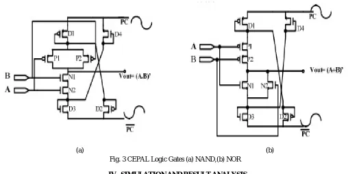
(a) (b) Fig. 3 CEPAL Logic Gates (a) NAND,(b) NOR
IV. SIMULATIONANDRESULTANALYSIS
[image:4.612.56.564.76.330.2]Schematic of conventional CMOS 28T full adder is connected in cadence Virtuoso Schematic editor as shown below,
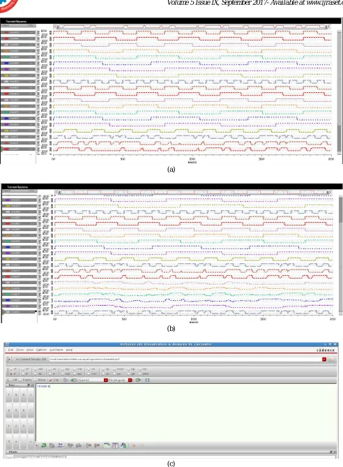
The transient analysis (inputs and outputs) of the above 28T Full adder is given by
Fig.4 inputs and outputs of Conventional 28T Full adder circuit
The logic gates are designed using CEPAL with energy recovery circuit and sinusoidal power supply , and they are connected as full adder shown in below fig.
(b)
Fig.4. CEPAL full adder (a) Schematic (b) Input and outputs waveforms Schematic of 8-bit CEPAL CSLA is connected as shown below
(a)
(b)
(c)
[image:7.612.66.558.53.722.2]TABLE I:RESULT ANALYSIS
CSLA Parameter Using 28T full
adder
Using CEPAL full adder
Bits 4-Bits 8-Bits 4-Bits 8-Bits
Power consumption 104.1µ W 351.1µ W 4.617µ W 10.82 µW Comparison of previously published work with this work is given by
TABLEII:COMPARISON WITH PREVIOUSLY PUBLISHED WORK
Parameter 2014 IJEERT [2]
2015 IJEDR [3] This work Using 28T FA
This work using CEPAL
Bits 8-bits 8-bits 8-Bits 8-Bits
Technology 180nM 180nM 180nM 180nM
Power consumption
13.77 µW 73.522 µW 351.1µW 10.82 µW
V. CONCLUSIONS
Hence, The design of 8-bit CSLA using Complementary Energy Path adiabatic logic is presented in this paper using cadence virtuoso spectre simulator with 180nM CMOS technology(gpdk 180) and achieved the power consumption 10.82 µW for overall 8-bit CSLA. And The results also proves that the CEPAL is suitable for optimal speed performance applications. Now a day’s power, area and performance are most valuable point in electronics world, even though area increased in the CEPAL technique there is a good tradeoff observed between the power and area.In future this technique will be the promising technique for design of power efficient circuits.
REFERENCES
[1] Manash Chanda,Sankalp Jain, Chandan Kumar Sarkar “Implementation of Subthreshold Adiabatic logic for ultralow power Application”, IEEE 2015. [2] Yogita Hiremath " A Novel 8-bit Carry Select Adder using 180nm CMOS Process Technology" International Journal of Emerging Engineering Research and
Technology Volume 2, Issue 6, September 2014.
[3] G.Venkatrao and B.Jugal Kishore " Design of Area-Delay-Power Efficient Carry Select Adder Using Cadence Tool", at IJEDR, Volume 3, Issue 3, ISSN: 2321-9939 ,2015.
[4] R.T.Hinman and M.F.Schlecht.”Recovered energy logic-A highly efficient alternative to Today’s logic circuits”,IEEE power Electronics Specialists Conf.,1993. [5] N.Swaruparani and A.Prasad.”Simulation of Complementary Energy Path Adiabatic Logic Based Sklansky tree adder design”,
IJEC,volume.7,pp.551-556,Nov2014.
[6] M.Rajesh,R.Manikandan,”Efficient Implementation of Carry Select Adder”APRN journal Of Science and Technology,Vol 3,No.2,Feb-2013.