ScholarWorks @ Georgia State University
ScholarWorks @ Georgia State University
Chemistry Dissertations Department of Chemistry
Fall 11-12-2012
Electrochemical Characterizations and Theoretical Simulations of
Electrochemical Characterizations and Theoretical Simulations of
Transport Behaviors at Nanoscale Geometries and Interfaces
Transport Behaviors at Nanoscale Geometries and Interfaces
Juan Liu
Follow this and additional works at: https://scholarworks.gsu.edu/chemistry_diss
Recommended Citation Recommended Citation
Liu, Juan, "Electrochemical Characterizations and Theoretical Simulations of Transport Behaviors at Nanoscale Geometries and Interfaces." Dissertation, Georgia State University, 2012.
https://scholarworks.gsu.edu/chemistry_diss/74
This Dissertation is brought to you for free and open access by the Department of Chemistry at ScholarWorks @ Georgia State University. It has been accepted for inclusion in Chemistry Dissertations by an authorized
administrator of ScholarWorks @ Georgia State University. For more information, please contact
AT NANOSCALE GEOMETRIES AND INTERFACES
by
JUAN LIU
Under the Direction of Dr. Gangli Wang
ABSTRACT
Since single nanopores were firstly proposed as a potential rapid and low-cost tool for DNA
se-quencing in 1990s (PNAS, 1996, 93, 13770), extensive studies on both biological and synthetic
na-nopores and nanochannels have been reported. Nanochannel based stochastic sensing at single
molecu-lar level has been widely reported through the detection of transient ionic current changes induced by
geometry blockage due to analytes translocation. Novel properties, including ion current rectification
(ICR), memristive and memcapacitive behaviors were reported. These fundamental properties of
na-nochannels arise from the nanoscale dimensions and enables applications not only in single molecule
sensing, but also in drug delivery, electrochemical energy conversion, concentration enrichment and
separation, nanoprecipitation, nanoelectronics etc. Electrostatic interactions at nanometer-scale
be-tween the fixed surface charges and mobile charges in solution play major roles in those applications
na-The determination of SCD at nanometer scale is urgently needed for the interpretation of
aforemen-tioned phenomena. This dissertation mainly focuses on the determination of SCD confined at a
na-noscale device with known geometry via combined electroanalytical measurements and theoretical
simulation. The measured currents through charged nanodevices are different for potentials with the
same amplitude but opposite polarities, which deviates away from linear Ohm’s behavior, known as ICR.
Through theoretical simulation of experiments by solving Poisson and Nernst-Planck equations, the SCD
within nanoconfinement is directly quantified for the first time. An exponential gradient SCD is
intro-duced on the interior surface of a conical nanopore based on the gradient distribution of applied electric
field. The physical origin is proposed based on the facilitated deprotonation of surface functional groups
by the applied electric field. The two parameters that describe the non-uniform SCD distribution:
maxi-mum SCD and distribution length are determined by fitting high- and low-conductivity current
respec-tively. The model is validated and applied successfully for quantification and prediction of mass
transport behavior in different electrolyte solutions. Furthermore, because the surface charge
distribu-tion, the transport behaviors are intrinsically heterogeneous at nanometer scale, the concept is
extend-ed to noninvasively determine the surface modification efficacy of individual nanopore devices.
Prelimi-nary results of single molecule sensing based on streptavidin-iminobiotin are included. The pH
depend-ent binding affinity of streptavidin-iminobiotin binding is confirmed by differdepend-ent currdepend-ent change signals
(“steps” and “spikes”) observed at different pHs. Qualitative concentration and potential dependence
have been established. The chemically modified nanopores are demonstrated to be reusable through
regenerating binding surface.
AT NANOSCALE GEOMETRIES AND INTERFACES
by
JUAN LIU
A Dissertation Submitted in Partial Fulfillment of the Requirements for the Degree of
Doctor of Philosophy
in the College of Arts and Sciences
Georgia State University
Copyright by Juan Liu
AT NANOSCALE GEOMETRIES AND INTERFACES
by
JUAN LIU
Committee Chair: Gangli Wang
Committee: Jenny J Yang
Stuart Anthony Allison
Electronic Version Approved:
Office of Graduate Studies
College of Arts and Sciences
Georgia State University
DEDICATION
ACKNOWLEDGEMENTS
All of my work has been done under the direction of my PhD advisor Dr. Gangli Wang. I owe my
deepest gratitude to Dr. Wang. He enlightens my research on nanopores and is extreme patient on
men-toring me. He teaches me the way to apply book knowledge into practical application. Most important
he also teaches me the way of thinking and doing research. What he had taught me will benefit both
research and life. It’s my great honor to be Dr. Wang’s student.
I appreciate my committee members: Prof. Jenny J Yang, Prof. W. David Wilson and Prof. Stuart
Anthony Allison for their helpful suggestions.
I thank all the lab members in Dr. Gangli Wang’ group: Maksim Kvetny, Dengchao Wang,
Zhenghua Tang, Yan Li, Warren Brown, Tarushee Ahuja, Cecil Conroy and other lab members. I really
enjoy the life in the lab together with them.
I also want to thank Dr. Baohua Wu on the help of COMSOL Multiphysics, Dr. Hui Zhao for using
AFM, Yidan Liu and Dr. Jie Jiang for providing me samples.
My friends: Xue Qi, Nan Zhao, Qian Wang, Juan Sun and Guchuang Yang have accompanied my
PhD life; I appreciate the time with them.
I acknowledge the fellowship from Molecular Basis of Disease Area of Focus (2011-2012),
Geor-gia State University. The financial supports from GWang startup at GSU, Research Initiation Grant at GSU
TABLE OF CONTENTS
ACKNOWLEDGEMENTS ... v
LIST OF SCHEMES ... x
LIST OF TABLES ... xi
LIST OF FIGURES ... xii
1 INTRODUCTION ... 1
1.1 The fabrication of nanochannels and microchannels ... 3
1.1.1 Biological ion channels ... 3
1.1.2 Microchannels ... 3
1.1.3 Nanochannels ... 4
1.1.4 Arrays and membranes ... 6
1.2 Stochastic sensing based on nanodevices ... 7
1.2.1 The Coulter Counter ... 7
1.2.2 Polymer sensing ... 7
1.2.3 Nucleic acid sensing ... 8
1.2.4 Protein, nanoparticle and other molecule sensing ... 9
1.2.5 Adavantages of channel-type nanodevice based sensing ... 10
1.2.5.1 The ultimate sensitivity―single molecule ... 11
1.2.5.2 Heterogeneity analysis ... 11
1.2.5.3 Label-free analytes ... 12
1.2.6 Challenges in DNA sequencing ... 12
1.3 Microchannels and Nanochannels in other applications ... 13
1.3.1 Nanofluidic electronics ... 13
1.3.3 Drug delivery ... 15
1.3.4 Electrochemical energy conversion ... 15
1.3.5 Spatially confined nanoprecipitation ... 16
1.4 Novel properties of nanopore ... 16
1.4.1 Ion current rectification ... 17
1.4.2 Memristive and memcapacitive ion transport ... 18
1.5 Theoretical studies of ion transport through single nanopores and nanochannels ... 19
1.5.1 Molecular dynamics simulation ... 20
1.5.2 Finite element simulation based on continuum theory ... 23
2 GLASS NANOPORES AS SINGLE MOLECULE BINDING SENSORS ... 23
2.1 Introduction ... 23
2.2 Preliminary results and discussion ... 25
2.2.1 Streptavidin binding with iminobiotin modified glass nanopores ... 25
2.2.1.1pH dependence ... 26
2.2.1.2Concentration dependence ... 27
2.2.1.3Potential dependence ... 28
2.2.1.4Counting the binding sites and binding surface regeneration ... 29
2.2.2 The binding of streptavidin-DNA aptamer conjugate ... 30
2.2.3 Challenge in nanodevice based stochstic sensing-data comparison ... 34
2.3 Experimental details ... 35
2.3.1 Materials ... 35
2.3.2 Nanopore fabrication and surface modification ... 36
2.3.3 Electrochemical measurements ... 40
3 SURFACE CHARGE DENSITY DETERMINATION OF SINGLE CONICAL NANOPORES BASED ON
NORMALIZED ION CURRENT RECTIFICATION ... 42
3.1 Introduction ... 42
3.2 Results and discussion ... 46
3.2.1 Experiments: normalized conductivity in potential scanning measurements ... 46
3.2.2 Simulation based on continuum theory ... 48
3.2.2.1Spatial distribution of ion concentration inside the nanopores ... 50
3.2.2.2Spatial distribution of ion flux inside nanopores ... 53
3.2.2.3Quantification of the effective SCD of individual nanopores. ... 56
3.2.2.4Transference number of K+ and Cl- in high- and low-conductivit states ... 58
3.3 Experimental section ... 59
3.3.1 Materials ... 59
3.3.2 Conical nanopore fabrication and surface modification ... 60
3.3.3 Electrochemical measurements ... 60
3.3.4 Theoretical simulation ... 61
3.4 Summary ... 63
4 ELECTRIC FIELD DEPENDENT SURFACE CHARGE DENSITY DISTRIBUTION IN SINGLE CONICAL NANOPORES ... 65
4.1 Introduction ... 65
4.2 Results ... 69
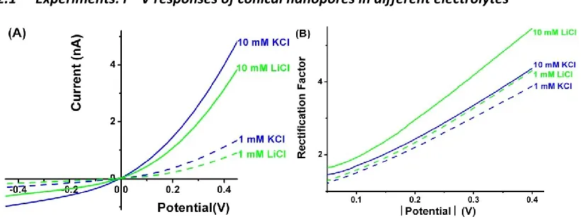
4.2.1 Experiments: i―V responses of conical nanopores in different electrolytes ... 69
4.2.2 Simulation based on continuum theory ... 71
4.2.3 Simulation of the measured current at high and low conductivity states ... 72
4.2.5 The tolerance of the effective SCD profile determined from i ―V measurements 77
4.2.6 The transference number of cations and anions at high- and low- conductivity
states... ... 79
4.3 Discussion ... 81
4.4 Experimental section ... 88
4.4.1 Materials ... 88
4.4.2 Conical nanopore fabrication and surface modification ... 88
4.4.3 Electrochemical measurements ... 89
4.4.4 Simulation ... 89
4.5 Summary ... 91
5 NONINVASIVE SURFACE COVERAGE DETERMINATION OF CHEMICALLY MODIFIED CONICAL NANOPORES THAT RECTIFY ION TRANSPORT ... 92
5.1 Introduction ... 92
5.2 Results and discussion ... 95
5.2.1 Experiments: i−V responses of conical nanopores ... 95
5.2.2 Correlation of the simulated current and SCD ... 97
5.3 Experimental section ... 101
5.3.1 Materials ... 101
5.3.2 Nanopore fabrication ... 102
5.3.3 Electrochemical measurements ... 102
5.3.4 Theoretical simulation ... 103
5.4 Summary ... 104
6 CONCLUSIONS AND SIGNIFICANCE ... 105
LIST OF SCHEMES
Scheme 2.1 Origin of negative charges on inner surface for a glass conical nanopore. Negative charges
result from deprotonation of surface silanol groups: ―SiOH SiO- + H+. ... 35
Scheme 2.2 Scheme of surface modification of a conical glass nanopore for targeting streptavidin. ... 40
Scheme 3.1 Ion Flux Confined by Nanopore Geometry and Interaction with the Fixed Charges at the
Glass-Solution Interface. The double arrow suggests the electrostatic interaction between mobile ions
and those fixed negative charges, which can be divided into two components along and normal to the
direction of ion flux. Not drawn to scale. ... 44
Scheme 4.1 A gradient SCD distribution inside a conical nanopore. The electric field intensity,
represented by the blue and red colors at both ends of the half cross-section of a nanopore, dropped
sharply at the first 1~2 µm inside the nanopore, indicated by the color transition. ... 68
Scheme 4.2 Surface deprotonation affected by the applied electric field and the formation of an
exponential gradient surface charge distribution. ... 84
Scheme 5.1 Surface structures of silica surface (panels A and B) and amine surface (modified with
LIST OF TABLES
Table 1.1 Comparison of biological and synthetic nanopores... 3
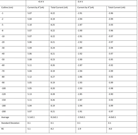
Table 3.1 Simulated current at different cutline positions under ±0.4 V bias potential (outside vs. inside) in 50 mMKCl solution. The surface charge density is at -170 mC m-2. The Cl- current is consistent at each cutline: +0.4 V, iCl- = 3.149±0.001 nA; -0.4 V, iCl- = -1.055±0.001 nA. The data were retained after Q test at 90% confidence level ... 55
Table 3.2 Summary of Simulated K+ and Cl- Contributions to the Transport Current ... 58
Table 3.3 Diffusion Coefficients of K+ and Cl- in Different KClSolutions ... 62
Table 4.1 Cation transference number based on an exponential SCD distribution ... 79
Table 4.2 The effective diffusion coefficient of K+ and Cl- ions in KCl solution ... 90
Table 4.3 The effective diffusion coefficient of Li+ and Cl- ions in LiCl solution ... 90
Table 5.1 The analysis of surface coverage of several chemically modified nanopores ... 100
Table 5.2 The SCD determined for different nanopores in 50 mMKCl at neutral pH (ca.6.2) ... 101
LIST OF FIGURES
Figure 2.1 Molecular structures of biotin (left) and 2-iminobiotin (right). ... 24
Figure 2.2 (Left panel) Streptavidin binding with anchored iminobiotin. Not drawn to scale. (Blue area
represents glass capillary, green triangles represent anchored iminobiotin, the purple tetramer
represent streptavidin). (Middle panel) i―t of streptavidin-iminobiotin binding within a 40 nm (radius)
conical nanopore in 0.1 M KCl, plus 20 mM PBS, pH 7.4. (Right panel) i―t of streptavidin-iminobiotin
binding within a 20 nm (radius) conical nanopore in 0.1 M KCl, plus 20 mM PBS, pH 6.6.. ... 26
Figure 2.3 Streptavidin-iminobiotin binding within a 40 nm conical nanopore in 0.1 M KCl, plus 20 mM
PBS at pH 7.4 with different streptavidin A) 0 nM (background) B) 0.2 nM C) 0.6 nM and D) 3 nM. Panel
E: Concentration dependence of streptavidin-iminobiotin binding at pH 7.4... ... 27
Figure 2.4 Streptavidin-iminobiotin binding within a 20 nm conical nanopore in 0.1 M KCl, plus 20 mM
PBS at pH 6.6 with different streptavidin A) 0.05 nM B) 0.25 nM and C) 2.5 nM. Panel D: Concentration
dependence of streptavidin-iminobiotin binding at pH 6.6... ... 28
Figure 2.5 Current change over time for streptavidin-iminobiotin binding within a 20 nm conical
nanopore in 0.1 M KCl, plus 20 mM PBS at pH 7.4 with 3 nM streptavidin under 0.2 V (left panel) and
-0.4 V (right panel) bias... ... 29
Figure 2.6 Binding sites quantification by counting “steps” and binding surface regeneration through
applying opposite potential to drive bound streptavidin out of single nanopores ... 29
Figure 2.7 (Panel A) i―t of 1:1 protein-DNA complex binding with anchored iminobiotin of a 50 nm
conical nanopore in 0.1 M KCl, plus 20 mM PBS, pH 6.6 under -0.4 V applied bias. (Panel B) Magnified
streptavidin-iminobiotin binding events from panel A. (Panel C) A scheme of 1:1 Streptavidin-Biotin
Immobilized DNA Aptamer Conjugate. Not drawn to scale. (Green triangle represents biotin group on
the DNA aptamer, curved red lines represents the single strand DNA 90mer, and the purple tetramer
Figure 2.8 Potential dependence of current change amplitudes of 1:1 protein-DNA complex binding with
iminobiotin functionalized nanopore sensor. ... 33
Figure 2.9 Potential dependence of current change duration of 1:1 streptavidin-biotin immobilized DNA
aptamer conjugate binding with iminobiotin ... 34
Figure 2.10 Cyclic voltammogram of a nanodisk electrode in 2 mM ferrocene with 0.1 M TBAP
acetonitrile solution ... 38
Figure 2.11 Cyclic voltammogram of a conical glass nanopore in 1 M KCl solution. ... 39
Figure 3.1 Normalized conductivity plots of a 26-nm-radius nanopore in different KCl solutions. The
current was normalized on the basis of concentration, with the factor listed next to each curve: (red)
0.01 M, X100; (blue) 0.05 M, X20; (green) 0.10 M, X10; (black) 1.00 M, X1. The scan rate was 20 mV/s. 44
Figure 3.2 Normalized conductivity curves of A: 161-nm-radius B: 123-nm-radius nanopore in KCl
solutions at different concentration: red 0.01 M, blue 0.05 M, green 0.10 M, black 1.00 M. The current is
normalized by the factors listed next to each curve based on the concentration. The nanopore surface
was modified with 3-aminopropyldimethylethoxysilane, which is found to offer more reproducible
measurements as previously described. ... 47
Figure 3.3 Electric conductivity at +0.4 V (red) and -0.4 V (black) along the centerline of a 26-nm-radius
nanopore in 50 mMKCl with surface charge density at -170 mCm-2. ... 48
Figure 3.4 The effects of nanopore radius and half cone angle on simulated current at +0.4 V (red
square) and -0.4 V (blue square). The half-cone angle is 11.2o in Panel A at 1 M KCl solution. The radius
is 26 nm in Panel B at 0.1 M KCl solution. ... 49
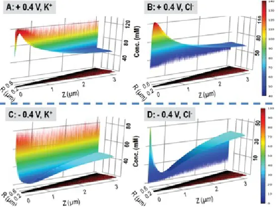
Figure 3.5 Concentration profiles of K+ (red) and Cl- (green) at (A) + 0.4 and (B) -0.4 V at cut line z = -100
nm. The x axis represents the distance away from the center line along the cut line. The radius of the
3.9). The bulk concentration of KCl is 50 mM. The intercept on the concentration axis is enlarged in the
inset panel. ... 50
Figure 3.6 Concentration profiles of K+ (red) and Cl- (green) at A: +0.4 V; and B: -0.4 V along centerline.
Negative values on x axis represents the depth inside the pore, with pore orifice at zero. The radius of
the nanopore is set at 26-nm with surface charge density defined at -170 mCm-2 (value based on Figure
3.9). The bulk concentration of KCl is 50 mM. The maximum and minimum concentration of each ion
(overlapped) along Z direction can be seen in the enlarged panel shown on the right. ... 50
Figure 3.7Spatial distribution of K+ and Cl- concentrations inside a nanopore for a 26 nm GNP in
50mMKCl with -170 mC m-2 SCD. The half-cross section nanopore geometry is shown at the bottom of
each panel. The adaptive mesh elements are much denser near the charged interface (boundary 5). The
nanopore orifice is at Z = 0 nm, and center line is at R = 0 nm. The concentration profiles inside the
nanopore at 3 μm and beyond continuously extend those features shown and thus are not included. The
top color scale applies to panels A and B, and the bottom color scale applies to panels C and D. Note that
the brushlike features near the interface resulted from the cut-off concentration range, which was set
during plotting for a better view. The absolute values at representative positions can be found in Figures
3.5 and 3.6. ... 52
Figure 3.8 Flux distribution of K+ (red squares) and Cl- (green triangles) at (A) +0.4 and (B) -0.4 V at cut
line z = -10 nm and at (C) +0.4 and (D) -0.4 V at cut line z = -100 nm. The x axis represents the distance
away from the center line along the cut line. The radius of the nanopore is set at 26 nm with the surface
charge density defined at -170 mCm-2 (value based on Figure 3.9). The bulk concentration of KCl is 50
mM. The intercept on the flux density axis is enlarged in the inset panel.. ... 53
Figure 3.9 Measured conductivity (solid black line) from a ca. 26-nm-radius nanopore in KCl solution at
different concentrations. Simulation results for the 26-nm-radius nanopore in (A) 1.00, (B) 0.10, and (C)
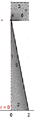
Figure 3.10 A typical adaptive free triangular mesh used in numerical simulation. ... 62
Figure 3.11 Comparison of the computed and measured current from a 26 nm nanopore in 1 M KCl
solution. Black symbols represent data calculated with diffusion coefficient at infinite diluted KCl
solution. The red symbols represent the data from the effective diffusion coefficient listed in Table 1.
Black line is the measured current-voltage curve in 1 M KCl solution. ... 64
Figure 4.1 A. Conductivity of a 46-nm-radius nanopore in KCl (blue) and LiCl (green) solutions at different
concentration: 10 mM (solid line) and 1 mM (dashed line). Scan rate was at 20 mV/s. B. The ratio of i+/i
-(RF) versus absolute potential amplitude. ... 69
Figure 4.2 Cyclic voltammograms (solid line) and theoretical simulation (symbols) of a 46 nm nanopore
in 1 M electrolyte solution. The simulation parameters for 1 M KCl (blue): -100 mC m-2 constant SCD
(circle); SCD linearly decreased from -100 mC m-2 to -1 mC m-2 within 0.94 µm (pentagon); -1 mC m-2
constant SCD (triangle). The simulation parameters for 1 M LiCl (green): -120 mC m-2 constant SCD
(circle); SCD linearly decreased from -120 mC m-2 to -1 mC m-2 within 1 µm (pentagon); -1 mC m-2
constant SCD (triangle). ... 70
Figure 4.3 The simulation of the experimental current from a 46-nm-nanopore in 10 mM KCl with
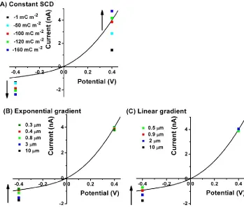
different SCD definitions on the interior surface. A. with a constant SCD uniformly distributed. B. an
exponentially decreased SCD, with σo=-100 mC m-2 and the distribution length varied as indicated in the
plot. C. a linearly decreased SCD, with σo=-100 mC m-2 and the distribution length varied as indicated in
the plot. ... 73
Figure 4.4 The simulation of the experimental current from a 26-nm-nanopore in 50 mM KCl with an
exponentially decreased SCD, with σo=-170 mC m-2 and the distribution length varied as indicated in the
plot. ... 74
Figure 4.5 The optimized simulation of the measured i―V curves with a 46 nm nanopore based on an
experimentally and the symbols were from the simulation. Fitting parameters: σo = -100 mC m-2 and τ =
0.4 µm for 10 mM KCl; σo = -70 mC m-2 and τ = 1.46 µm for 1 mM KCl; σo = -120 mC m-2 and τ = 0.4 µm
for 10 mM LiCl; σo = -70 mC m-2 and τ = 1.46 µm for 1 mM LiCl. ... 75
Figure 4.6 The optimized simulation of the measured i―V curves with a 46 nm nanopore based on a
linear SCD distribution in A. KCl and B. LiCl solutions. The solid curves were measured experimentally
and the symbols were from the simulation. Fitting parameters: σo = -100 mC m-2 and τ = 0.94 µm for 10
mM KCl; σo = -70 mC m-2 and τ = 3.6 µm for 1 mM KCl; σo = -120 mC m-2 and τ = 1 µm for 10 mM LiCl; σo =
-70 mC m-2 and τ = 3.6 µm for 1 mM LiCl. ... 76
Figure 4.7 Cyclic voltammogram (solid line) and optimized theoretical simulation (red squares) of a 26
nm nanopore (left panel) in 50 mM KCl and a 110 nm nanopore (right panel) in 100 mM KCl based on an
exponential gradient SCD. Fitting parameters: σo= -170 mC m-2, τ= 0.6 µm for the 26 nm nanopore; σo=
-480 mC m-2, τ= 2 µm for the 110 nm nanopore. ... 78
Figure 4.8 Error analysis of the maximum SCD σo at the nanopore orifice and the distribution length τ in
the simulation of i―V measurements of a 46 nm GNP in 10 mM KCl. A. high conductivity states at +0.4
V. B. low conductivity state at -0.4 V. Different colors represent different σo: -90 mC m-2 (blue); -100 mC
m-2 (red); -110 mC m-2 (green). Solid symbols represent the simulation based on an exponential SCD
distribution, and open ones representing a linear SCD distribution. ... 79
Figure 4.9 The impacts of distribution length on the simulated current at A: high conductivity state at
+0.4 V and B: low conductivity state at -0.4 V. Data collected from a 46 nm nanopore in 1 mM KCl with
maximum SCD set at -70 mC m-2. ... 81
Figure 4.10 The concentration profiles along radial direction of K+ (blue) and Cl- (red) at A: + 0.4 V; and B:
-0.4 V at cutline z = 100 nm. The x axis represents the distance away from the centerline along the
-1 mC m-2 within 0.4 µm (value based on Figure 4.3). The bulk concentration of KCl is 10 mM. The
intercept on the concentration axis is enlarged in the inserted panels. ... 81
Figure 4.11 Concentration profiles of K+ (red) and Cl- (green) at A: + 0.4 V; and B: -0.4 V along centerline.
The radius of the nanopore is set at 46-nm with surface charge density defined at -100 mC m-2 to -1 mC
m-2 within 0.4 µm (value based on Figure 4.3). The bulk concentration of KCl is 10 mM (indicated by
black dash line). The concentration of K+ and Cl- overlapped. ... 82
Figure 4.12 Electric field intensity distributions (solid lines) for a 46 nm conical nanopore with neutral
surface in 10 mM KCl. (A) centerline and (B) a parallel cutline 3 nm from the interior surface at -0.4 V.
The dash lines are exponential fittings of the electric field intensity profiles. Electric field intensity
distributions through the whole pore are shown in inserted panels. Pore depth at 0 and 10 μm
correspond to the location of orifice and base respectively. ... 83
Figure 4.13 Electric field intensity distributions (solid lines) for a 46 nm conical nanopore with neutral
surface in 10 mM KCl. (A) centerline and (B) a parallel cutline 3 nm from the interior surface at -0.2 V.
The dash lines are exponential fittings of the electric field intensity profiles. Electric field intensity
distributions through the whole pore are shown in inserted panels. Pore depth at 0 and 10 μm
correspond to the location of orifice and base respectively. ... 83
Figure 4.14 Electric field intensity distributions (solid lines) for a 46 nm conical nanopore with neutral
surface in 10 mM KCl. (A) centerline and (B) a parallel cutline 3 nm from the interior surface at +0.4 V
(red) and +0.2 V (blue). Pore depth at 0 and 10 μm correspond to the location of orifice and base
respectively. ... 85
Figure 4.15 The electric field intensity along the cutlines parallel to nanopore interior surface and the
comparison with the SCD profile (dash line). The results are from a 46 nm nanopore in 10 mM KCl. The
overall electric field Etot is divided by the listed factor for direct comparison of the gradient distribution.
Figure 4.16 The electric field intensity along the centerline and the comparison with the SCD profile
(dash line). The results are from a 46 nm nanopore in 10 mM KCl. The overall electric field Etot is divided
by the listed factor for direct comparison of the gradient distribution. ... 86
Figure 4.17 The electric field intensity along the cutlines parallel to nanopore interior surface and the
comparison with linear SCD profile (dash line). The results are from a 46 nm nanopore in 10 mM KCl. The
overall electric field Etot is divided by the listed factor for direct comparison of the gradient distribution.
... 87
Figure 4.18 The variation of nanopore geometry near the pore orifice.The dash line indicates the
geometry before distortion. ... 95
Figure 5.1 The i―V curves from a 32-nm-radius nanopore in 50 mMKCl pH 3 (red) and pH 9 (blue)
solutions. (A) silica surface and (B) surface modified with 3-aminopropyldimethylethoxysilane. The
scattered symbols represent the simulated current computed from the optimized surface charge
parameters discussed later. The dashed line represents the volume conductivity calculated based on
geometric resistance in 50 mMKCl. ... 97
Figure 5.2 The i―V curves from a 50-nm-radius nanopore before (silica surface) and after (amine
surface) modification with 3-aminopropyldimethylethoxysilane in 50 mMKCl solutions in different pH
conditions. The solution pH was determined by a pH meter and adjusted by the addtion of concentrated
HCl or KOH solutions.The dash line represents the volume conductivity of the same nanopore geometry
in 50 mM calculated based on pure geometric resistance. ... 98
Figure 5.3 Correlation between the simulated current and SCD at +0.4 V applied potential for a 32-nm
radius nanopore in 50 mMKCl. A linear fitting (R2 = 0.99) is shown as the red dashed line. ... 98
Figure 5.4 The correlation between the simulated current and SCD at +0.4 V applied potential of a (A)
mM (green); 200 mM (blue) and 500 mM (magenta) KCl solutions. Linear fittings for each concentration
are indicated by dashed lines. ... 98
Figure 5.5 The correlation between the simulated current and SCD at +0.2 V applied potential of a
26-nm-radius (silica surface, without modification) nanopore in 50 mM (red); 100 mM (green); 200 mM
(blue) and 500 mM (magenta) KCl solutions. Linear fittings for each concentration are indicated by
dashed lines. ... 99
Figure 5.6 Site density (SCD: the combination of deprotonated silanol groups and protonated amine
groups) of the nanopores with different radii with (top panel) amine surface (surface modified with
3-aminopropyldimethylethoxysilane) and (bottom panel) silica surface in 50 mMKCl at different pHs. The
site density is calculated based on the SCD determined from the experimental current trajected from the
linear trend for each nanopore at +0.4 V applied potential. ... 99
1 INTRODUCTION
What is a nanopore or nanochannel? A nanopore or nanochannel is a small pore or channel
connecting two solution reservoirs with the radius less than 100 nm in at least one dimension.
Na-nopores and broadly defined channel-type nanodevices have attracted extensive research interest in the
past two decades. The nanopores were proposed as a potential tool for rapid DNA sequencing in the
1990s.1 Because different DNA bases have different conductivities, the DNA bases might be read out
sequentially (one by one base) when single strand DNA passes through the nanodevices in a linear form
if sufficient resolution could be reached. The first nanopore based experimental work was reported by
Kasianowicz and co-workers in 1996,2 using a biological nanopore: α-haemolysin, which is a
transmem-brane protein embedded in a lipid bilayer memtransmem-brane separating two solutions. The translocation of
nu-cleotides through α-haemolysin was indicated by the transient blockage of ionic current compared to a
clean background without nucleotides as the analyte. Extensive work has been done based on the
na-nopore formed in the α-haemolysin molecule situated in a lipid bilayer membrane.3-6
For bimolecular sensing based on biological nanopores, α-haemolysin has been widely used
based on its stability and excellent performance under physiological conditions. To accommodate for
more harsh measurement conditions, synthetic solid-state nanopores have been developed. Extensive
work has been done based on solid-state nanopores which allow easier handling for measurement.
Un-like α-haemolysin where the narrowest part only allows the translocation of ss-DNA, ds-DNA transport
through a solid-state nanopore has been first reported by Golovchenko’s group.7 Due to rapid
develop-ments on fabrication and characterization of synthetic solid-state nanopores, explosive progresses have
been achieved on studying ss/ds-DNA translocations.8-15 The difference between polyA and polyC RNA
with a heterogeneous sequence of A30C70 could also be distinguished. These achievements make
nanodevices promising for DNA sequencing.
Synthetic nanopores and α-haemolysin based biological nanopores can be used for single
mo-lecular sensing and ultimately developed as a rapid and economical tool for DNA sequencing.
Mean-while, nanopores and other channel-type geometries, also have potential application in drug delivery,
electrochemical energy conversion, nanofiltration, purification and catalysis, concentration and
separa-tion, nanofluidic electronics, nanoprecipitation and so on.
Besides the above discussed sensing applications at single molecular level, novel mass transport
properties of nanodevices also attracted tremendous interest. Mass transport inside nanometer scale
devices is determined by both geometry and solution-substrate interface factors (i. e. coulomb
interac-tions between solution ions and surface charges). At high surface to volume ratio, a significant
contribu-tion from surface leads to several important properties of nanodevices, such as ion current rectificacontribu-tion
(ICR),17,18 memristive and memcapacitive behaviors. These novel properties suggest nanopores and
oth-er nanodevices to be fundamentally important for the enhancement of electrochemical enoth-ergy convoth-er-
conver-sion efficacy in batteries and supercapacitors,19-21 and to be used as nanoelectronics.17,22
For mass transport at nanometer scale dimension, due to the high surface to volume ratio, the
surface will contribute even dominate the mass transport behavior in comparison to volume effect,
which complicates the interpretation of nanodevices based stochastic sensing and ICR, memristive and
memcapacitive behaviors. To obtain a better understanding of the mass transport behavior at nanoscale
geometries, theoretical simulation has been implemented. The physical origins of ICR have been
ex-plained based on the non-uniform ion distribution induced by asymmetric nano-geometries with
charged surface, heterogeneous surface charge distribution within a nano-geometry etc. Massive
theo-retical works with a constant SCD using finite element method based on continuum theory have been
1.1 The fabrication of nanochannels and microchannels
1.1.1 Biological ion channels
Some protein ion channels are suitable for single molecule sensing due to their natural channel
dimensions being comparable to the size of targeted analytes. Among those biological nanochannels,
α-haemolysin situated in a lipid bilayer is by far the most widely used for studying DNA translocations.
1-3,6,26
α-haemolysin is a transmembrane protein, with a diameter of 1.4 nm at the narrowest part.
Thus α-haemolysin based nanochannels will only allow translocation of single-strand DNA due to this 1.4
nm dimension limitation at the nanochannel center, double-stranded DNA (~2 nm diameter) has larger
dimensions than the pore and is unable to pass through.
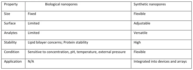
Due to limitations of biological nanopores, summarized in table 1.1, synthetic nanochannels and
[image:25.612.105.507.428.575.2]microchannels have been developed which can be superior to biological nanopores in several aspects.
Table 1.1 Comparison of biological and synthetic nanopores
Property Biological nanopores Synthetic nanopores
Size Fixed Flexible
Surface Limited Adjustable
Analytes Limited Versatile
Stability Lipid bilayer concerns; Protein stability High
Condition Sensitive to concentration, pH, temperature, external pressure Flexible
Application N/A Integrated into devices and arrays
1.1.2 Microchannels
In the past thirty years, microchannels with dimension less than 100 µm have attracted
exten-sive interests. Microfluidics, also known as lab-on-a-chip technology is a technique that requires precise
control and manipulation of fluids at micro liter scale, has shown broaden applications in biology,
for developing countries, Whitesides at Harvard University has beendedicated to developing
microfluid-ics based low-cost medical diagnostic devices. Microfluidmicrofluid-ics devices are created using silicon, plastic
chips and finally paper is chosen due to its cheap price and is easily disposed by incineration which is
convenient for medical waste disposal.33-37 Meanwhile, Ramsey at UNC has done a lot of work on
micro-fluidics based MSI-MS,38,39 sample filtration, concentration and separation,40-42 and single cell analysis.43
Microchannels are mostly fabricated based on ion beam lithography, electron beam lithography
and photolithography.44-46 Basically a convex three-dimension mold is created by shattering a beam of
ions/electrons or photons onto a positive resist film supported by substrate, with the desired part
cov-ered by a mask. The obtained mold is then coated with a layer of negative resist. Later the mold and the
support substrate are etched away, which leaves the designed geometry with micrometer dimension in
the coated film replicating the shape of mold. Polydimethylsiloxane (PDMS) and other polymers are
mainly used in this soft lithography, as polymer based fabrication is easier and flexible, also the price is
much cheaper than silicon and glass.
Other fabrication techniques include reactive ion etching (RIE), laser ablation and imprinting. RIE
is also widely used for microfluidics fabrication, but with quite limited materials (glass, quartz and
sili-con). Microchannels made of glass by using a mixture of acid solution is used to etch the glass while
other parts covered with metal masks have been reported.47,48 Laser ablation, similarly to ion beam
li-thography, involves a shining of laser to polymer substrate which results in polymer decomposition. A
cavity is created as decomposition products (CO2, CO and C2H2) are ejected.49 Another simple
microfluid-ics fabrication is called imprinting. Generally a micrometer size wire is pressed into a polymer substrate,
results in a microchannel in the polymer substrate replicating the wire geometry.44
1.1.3 Nanochannels
As summarized in Table 1.1, synthetic nanochannels/nanopores are more resistive to harsh
sur-face, rendering them with high versatility for targeting various analytes. Most important, synthetic
solid-state nanodevices are capable of being integrated into devices and arrays. All of these advantages have
stimulated the development of synthetic nanodevices.
Synthetic nanopores can be made from different kinds of materials such as silicon oxide
(SiO2),50,51 silicon nitride (SiN),7 aluminum Oxide (Al2O3),52 polymers22 and graphene.53 The solid state
nanopores are more robust compared to biological nanopores that are sensitive to pH, pressure and
temperature. Recently a lot of success in preparing synthetic nanopores has been achieved. Similar to
microchannels, nanochannels are mostly fabricated based on ion beam lithography, electron beam
li-thography and photolili-thography as the mold size can be controlled down to nanometer scale resolution.
Typically these lithography based fabrication methods included: 1. “Track-etch” method22,54, and 2.
“Ion-beam sculpting” method7.
The “Track-etch” method uses commercially available polymer membrane with track damages
created by shooting heavy ions through a polymer membrane. Then the damaged polymer membrane is
etched in alkaline solution on one side, while on the other side a neutralizing electrolyte is used,
result-ing in a conical nanopore.22 The “Ion-beam sculpting” method is based on a solid-state insulating
mem-brane with a cavity on surface. An ion-beam is applied from the other side to remove memmem-brane
mate-rials until at the bottom of cavity a through pore is formed.7 The sculpting process is monitored by
com-puter. When a pore is obtained, single ions will transport through the pore and will be detected by the
detector. Then the ion beam sculpting process will be stopped immediately.
Besides these lithography based fabrication techniques, nanochannels can also be obtained
through the fabrication of carbon nanotubes and other nanotubes (titanium oxide, gold etc.)55-59. Carbon
nanotubes can be fabricated based on chemical vapor deposition (CVD), where nanotubes will be grown
In this dissertation, the “Bench-top” method is used for fabricating single conical glass
na-nopores using a glass capillary. Basically, a nanopore with pore opening less than 100 nm and a length
around ~10 µm is obtained by replicating the geometry of an electrochemically sharpened Pt nanotip.
1.1.4 Arrays and membranes
The techniques mentioned above are used for fabricating single microchannels or nanochannels.
To gain a high throughput, arrays of microchannels/nanochannels are created, which normally uses a
nanochannel array mold created by electron beam lithography and ion beam milling. Nanochannel
ar-rays are fabricated by pressing a nanochannel array mold into a resist film resulting geometry in the film
replicates the shape of the mold.60-63 Based on this concept, Chou’s group introduced a nanochannel
array fabrication method using “nanoimprinting lithography (NIL)”. The mold is fabricated by NIL
tech-niques with channel size can be manipulated down to 10 nm.64 Nanochannels fabricated without using
NIL techniques has been reported recently.62,65 Basically, A layer of nanometer thin amorphous silicon
film deposited and etched using RIE, followed by thermal oxidation. Solid channels with the outside to
composed of SiO2 of nanometer scale dimension (inside is silicon) are created in the film. Further
depo-sition of amorphous silicon and subsequent chemical-mechanical polishing will expose the gap oxide.
Nanochannels are obtained after etching away SiO2. Nanotube based arrays are also achieved using an
anodic alumina (AAO) template.66 Polypyrrole is deposited into the AAO template and further etching of
AAO resulted in a gap between the polypyrrole nanowires and AAO. Further deposition of gold and
sub-sequent etching of polypyrrole and AAO results in a gold nanotube array.
Meanwhile, nanoporous membranes have been developed, which are widely used in drug
deliv-ery, filtration, and purification.67-69 For example, Martin and co-workers reported a carbon nanotuble
1.2 Stochastic sensing based on nanodevices
1.2.1 The Coulter Counter
Nanochannels have been extensively studied due to the nanometer-scale and the resulting
nov-el mass transport behavior. The main motivation is the potential application in stochastic single
mole-cule sensing based on the Coulter Counter concept. The Coulter Counter was patented by W. H. Coulter
in 1953. A typical Coulter counter set up includes one or more microchannels or nanochannels
separat-ing two chambers of electrolyte solutions. With an external applied potential, particles present in
elec-trolyte solutions are driven through channels. The measured current is non-Faradic current, which
re-sults from the transport of ions (charge carriers) through the most resistive region of the channels. Thus
when particles with comparable size transport through the channels, they will partially block the
geome-try, which results in a significant transient ionic current blockage being detected/counted. Based on this
concept, nanopores and other nanochannels based stochastic sensing allows a single molecule
resolu-tion due to nanometer scale dimension which is comparable to single molecules.
1.2.2 Polymer sensing
Nanopores were first proposed as a potential rapid and economical tool for DNA sequencing.
The first experimental work was done by Kasianowicz and co-workers in 1996.2 The homo-polymers are
driven through the biological nanopore in a α-haemolysin molecule under external applied potential.
Before adding analytes, mobiles ions are electrophoretically driven through the nanopore resulting a
constant current (background/baseline), which is limited by the most resistive (the smallest) region.
When polymers or other analytes are added into solution, they will be driven into the biological
na-nopore also. As their sizes are comparable to the nana-nopore, their translocation will partially block the
pore. Thus mobile ions transported through the channel will decrease, causing the current to decrease.
analytes gives an ionic current blockage event. The current blockage frequency indicates analytes
con-centration: at high concentration, more analytes are present in solution and transported through the
nanochannels, thus more events will be observed within the same time. Meanwhile, the duration of
these transient current blockages resulting from molecule binding also provides the binding kinetic
in-formation. Different current blockade events induced by translocation of different polymers using
α-haemolysin protein nanopore are reported.6,16,70 The correlation between induced current blockages
and polymer composition, translocation orientation and applied bias has been studied by Gundlach and
co-workers.70 Recently, they demonstrated DNA sequencing at single nucleotide resolution using a
mu-tated MspA nanopore with phi29 DNA polymerase controlling the translocation velocity.71
Different noises associated with the measured current signals are observed for different PEG
polymers using α-haemolysin based nanopore, which suggest an interaction between channel lumen
and PEG polymers.72,73 The polymer-lumen interaction was showed to be controlled by pH which gives a
clue to optimize stochastic sensing.73 The translocation duration of different polymers has been studied
by Branton and co-worker,6 and the translocation duration showed a significant temperature
depend-ence. Biopolymer analysis based on nanochannel arrays has been patented recently.74
1.2.3 Nucleic acid sensing
As nanopores and nanochannels were mainly proposed as a potential DNA sequencing tool,
ex-tensive work based on DNA detection and characterization have been reported.6,8,9,11-14,16,75-78
Since the smallest region of α-haemolysin is only 1.4 nm in diameter, α-haemolysin based
na-nopores only allows the translocation of single-stranded DNA.6,76 Different DNA segments have been
driven electrophoretically through a nanopore, giving different translocation durations. The measured
translocation duration time is reported to be temperature dependent. Due to the limitations of
biologi-cal nanopores, synthetic nanopores are developed. Martin and co-workers demonstrate the
block-age induced by transient passblock-age of DNA is demonstrated to be concentration dependent. Meanwhile,
the duration of transit current change is reported to depend on the external applied transmembrane
potential. A much shorter duration of current blockage was observed when detecting a double-stranded
DNA; this is explained by the collision of double-stranded DNA with the nanopore orifice as the
na-nopore used is smaller than double-stranded DNA.
The transport of single strand DNA molecule labeled with nanoparticles through a glass
nanopi-pette has been reported.9 The nanopipette is fabricated by mechanically pulling a glass capillary upon
heating by a laser. The conjugate is often found to transiently enter the pore without a full
transloca-tion. Different translocation events are observed when DNA is transported through a ion beam sculpted
nanopore in different conformations.11 The current change amplitude and the corresponding duration of
translocation events induced by DNA translocation through a nanopore in different conformations are
different. The DNA translocation in unfolded form is found to increase as potential increase and as DNA
length increase.
With the development of solid-state nanopore fabrication, translocation of double-stranded
DNA through a 5 nm (diameter) nanopore has been achieved.7 While most analyte translocation through
nanopores/nanochannels are under a constant applied potential, DNA transport through a nanopore
using a AC signal has also been reported.75
1.2.4 Protein, nanoparticle and other molecule sensing
Besides nanopore based polymer and DNA sensing, both biological and synthetic solid-state
na-nopores have been used for the detection of proteins, nanoparticles, drug molecules, ions and
bio-interactions.
Li’s group reported protein characterization based on a single silicon nitride nanopore.79 BSA
and fibrinogen are differentiated based on different ionic current blockages induced by the two
time duration and integration of current change respect to time. The size of BSA is also confirmed by the
current changed induced by BSA translocation through a 55 nm (diameter) nanopore.80
White’s group reported translocation of nanoparticles with different radius (80 nm and 160 nm)
which consequently induce transient current blockages with different amplitude.81 Nanoparticle
detec-tion using carbon nanotubes have also been reported, the size and surface charge of nanoparticles are
determined simultaneously.82
A similar approach could be used for detecting organic molecules. Organic molecules sensing
based on a protein channel with a molecular adapter (cyclodextrins) located inside the nanochannels
through non-covalent binding have been reported by Bayley and co-workers.4 Different ions are
differ-entiated based on a mutated a-haemolysin nanochannel.83 Characterization and quantification of
diva-lent metal ions are achieved by using a mutated heteromeric α-haemolysin protein which allows metal
ion binding .84
1.2.5 Advantages of channel-type nanodevice based sensing
Many analytical tool and methods have been developed in the past, for example, fluorescent
spectrometry, high performance liquid chromatography (HPLC), and electrochemical analysis etc. By
re-peated sampling and/or signal amplification, the sensitivity of these techniques can reach as high as
picomole/fetomole or even higher. As a chemical or biological molecule is defined by a certain
composi-tion, the ultimate sensitivity to detect or analyze a sample would be a single molecule. Compared to
these ensemble techniques, the most striking advantage of nanopore based stochastic sensing is the
single molecule sensitivity rendered by the nanometer dimension. While for ensemble techniques, this
ultimate sensitivity is still missing as the detected signal from a unique molecule is screened by
thou-sands of other molecules in the sample. In addition to this major advantage, other advantages like
ap-plication in heterogeneity analysis, label-free analytes, reusability and potential apap-plication for DNA
1.2.5.1 The ultimate sensitivity-single molecule detection
Since the first experimental work done by Kasianowicz using α-haemolysin, stochastic single
molecule behaviors have been demonstrated. For nanopore based sensing, the single molecular
sensi-tivity results from their nanometer scale dimensions. The detected current signal results from the ion
movement through the nanoconfinement. If the nanodevice has a signal limiting dimension comparable
to the targeted analytes, then the analytes passing through the nanopore orifice will partially block the
ion transport, thus resulting in a significant current change to be detected. That is why nanopores and
channel-type nanodevices can be used for single molecule sensing. If the size of the analyte is larger
than nanopore dimension, the analyte will fully block the pore resulting in no background current. The
ability to resolve analyte at the single molecule limit has applications such as clinical diagnosis.
1.2.5.2 Heterogeneity analysis
Heterogeneity analysis is significantly important for human life. For example, cancer therapy,
which requires the early detection and characterization of mutated biomolecules. Resolution at the
sin-gle molecule limit by nanopore based sensing is the prerequisite for applications in heterogeneity
analy-sis. As the presence of analyte in solution is indicated by the transient ionic current blockage, the
heter-ogeneity of sample can be analyzed. Typically, the ionic current blockage can be described by two
pa-rameters: current change amplitude ∆i and time duration τ for each transient translocation event. The
current change amplitude indicates size and charge state of analytes. The time duration τ is the time it
takes analyte to traverse the most sensitive (current limited) region, which probably indicates the
ana-lytes structure/conformation. If the current change is induced by single molecule binding confined in
nanopores, then the time duration τ indicates the binding ability. If different analytes go through
na-nopores or bind to surface immobilized receptors, the two parameters (amplitude ∆i and time duration
1.2.5.3 Label-free analytes
Nanodevice based sensing is widely studied not only for single molecule sensitivity and potential
application in analyzing sample heterogeneity, but also for label-free analyte detection. Unlike other
single molecule detection techniques such as fluorescence imaging or radioisotope labeling, the analyte
is detected in the native state without any modification. Analytes present in solution can be driven by
the externally applied field due to electrophoresis if they are charged under the measurement
condi-tions. Since no analytes labeling/modification is involved, the nanodevice based sensing often requires
less sample and less time consuming sample preparation, thus it is more efficient and economical
com-pared to techniques which require labeling. More important, as the analytes are detected in their native
state, this excludes signal distortion introduced by molecule labeling or mutation.
Besides the sensitivity to detect single molecules, the sample heterogeneity analysis, and the
practical advantages in label-free analyte handling, nanodevices possess other advantages that make
them a powerful sensing tool. For example, fabricated solid-state nanodevices can be durable and
reus-able. Furthermore, as solid-state nanopores and nanodevices can be integrated into devices and arrays,
sensors based on solid-state nanodevices can be made as portable devices, as the whole set up simply
involves an external applied electric field through the sensing part. This is overwhelmingly competitive
than other related tools.
1.2.6 Challenges in DNA sequencing
Resolution at the single molecule level has been achieved in stochastic sensing applications
us-ing various nanodevices. The feasibility and efficacy of nanopore based rapid and low-cost DNA
se-quencing have been demonstrated. Significant progresses have been achieved.71 However, there are still
challenges to be resolved.
Typical biological nanopore systems involve a protein situated in a lipid bilayer membrane. The
bilayers are fragile. Meanwhile, lipid bilayers are sensitive to solution pH, electrolyte concentration,
pressure and temperature, thus do not last long. All of these concerns need to be resolved.
On the one hand, the detected intrinsic low current signal through nanodevices allows
resolu-tion of a single molecule. On the other hand, as the current is so small any noise from surrounding
envi-ronment arise as a major concern. Nanodevice performance can be improved through data averaging
which minimizes the noise. Further efforts in eliminating surrounding noise are still required.
To resolve a single base, the translocation duration of DNA through a nanopore should be equal
or larger than 1 millisecond based on Deamer and Branton’s report.3,85 Solutions for these concerns are
urgently needed. Recent work done by Gundlach and co-workers has demonstrated the ability to control
the DNA translocation at millisecond scale mediated by phi29 DNA polymerase inside a mutated MspA
nanopore.
1.3 Microchannels/Nanochannels in other applications
Besides single molecule detection, nanochannel devices have potential applications in many
ar-eas such as nanofluidics, nanoelectronics, concentration and separation, drug delivery, electrochemical
energy conversion, and controlled nanoprecipitation.
1.3.1 Nanofluidic electronics
Siwy, Martin and coworkers have pioneered studies of mass transport behaviors through
asym-metric nanochannel/nanopore devices.17,22,86,87 Controlled mass transport is achieved by changing the
geometry and surface charge distribution inside those nanodevices. For example, a bi-conical nanopore
with the narrowest part positioned at the center has been created. Bipolar surface charge has been
in-troduced in a conical nanopore, with positive surface charges on one end and negative charges on the
other end. A typical diode-like current-potential behavior has been observed in nanopores with different
polarity but allows a very low current to pass through at the opposite bias polarity. For a conical
na-nopore with a bipolar surface charge distribution, the “on” and “off” state can be switched by reverting
the distribution of opposite surface charges. The diode behavior can also be generated using a
cylindri-cal nanochannel with a unipolar surface charge distribution, where the channel is chemicylindri-cally modified so
that one side is positively charged while the other side is neutral.17 The control of mass transport
through solid nanodevices by designing the geometry and inner surface charge distributions enables
their application in nanofluidics and nano electronics.
1.3.2 Concentration and separation
Recently, Crook’s group reported the application in separation and electrolyte concentration
enhancement by bipolar electrodes (BPEs) created inside microchannels or nanochannels.88 A bipolar
electrode is composed of an electric conductor, normally a long nanowire in a conductive ionic
environ-ment inside a nanochanel/microchannel. Electron transfer processes, reduction or oxidation will occur
on either end of the conductor when a high electric field is created between the two ends of the
con-ductor. The conductor is normally supported on the insulating channel interior surface. Therefore there
is no direct connection between the conductor and external power supply. High throughput analysis can
be achieved with such simplified design. The ability of BPEs to change the local electric field allows
spe-cies to concentrate locally, which is the prerequisite for the separation of analytes. Since the mobility of
different electrolytes is different, the position of molecule concentration zone for different electrolytes
will be different in the channel, thus separation of analytes can be achieved. In the paper, 1, 3, 6,
8-pyrene tetrasulfonic acid (PTS4-), 8-methoxypyrene-1, 3, 6-trisulfonic acid (MPTS3-) and BODIPY2- were
separated based on the respective electrophoretic mobility. Other nanodevice based separations are
1.3.3 Drug delivery
Another important application of nanodevices is the application in drug delivery.89-92 The type of
nanopore membrane materials include silicon, poly (ethylene terephthalate) (PET) and polycarbonate
(PC) polymers, and etc. The nanopores are combined with a drug storing reservoir first. This combined
device is then implanted through direct injection using a specially designed trochar.93 A pump with a
ti-tanium chamber that can store drugs at a volume about 75-300 ml is introduced.94 The rigid titanium
shell allows easy implantation and removel, and titanium is resistive to body fluids for protecting the
stored drugs. At one end of the titanium chamber a silicon nanopore membrane is attached. The
na-nopore membrane is used for controlled drug delivery. Note if the nana-nopore size approaches the
dimen-sions of the drugs molecules, the release is not simply concentration-dependent, as the diffusion based
on Fick’s law of diffusion is not the sole transport mechanism. The size and density of nanopores in the
membrane could be designed for accommodating release of different drugs based on their sizes,
molec-ular structures, and other related properties. The nanopore pump is superior compared to the
commer-cially accessible Viadur/Duros devices, in which the drugs are released by an osmotic engine, thus
limit-ing the volume for drug storage.94
1.3.4 Electrochemical energy conversion
Most electrochemical energy conversion happens at the electrode surfaces. To increase the
en-ergy density for better device performance, high surface area electrodes are desired. Due to the high
surface to volume ratio at nanometer scale, the transport of cations and anions as charge carriers,
carry-ing the total current and quantified by the respective ion transference numbers, can be significantly
af-fected by the nanostructured geometries and interfaces. The selective transport of either cation or
ani-on could cause internal energy loss of energy devices. Fundamental understanding of iani-on transport
Kamat has reported a new generation of solar energy conversion device by using
nanostruc-tures.95 Three major ways are proposed: 1. Donor-acceptor assemblies for mimicking photosynthesis. 2.
Fuel production through semiconductor assisted photocatalysis. 3. Solar cells based on semiconductors
made of nanostructures. In each of those routes, the transport of charges will be significantly affected
by the nanostructures thus affecting the energy harvesting efficiency.
Recently, Jiang and co-workers reported an energy harvesting device by using a charged
na-nochannel.96 The maximum power for a single nanochannel is reported to be ~26 pW. A concentration
gradient at the two ends of a nanochannel with negatively charged surface is firstly established. This
device then converts Gibbs free energy in the form of diffusion current induced by concentration
gradi-ent into electric power. The obtained electric power shows a pH dependence, which allows for further
optimization for.
1.3.5 Spatially confined nanoprecipitation
If the electrolyte concentration is near saturation, the current measured using a nanopore will
oscillate due to the precipitation of electrolytes at the current limiting nanopore region.97 The
electro-lyte system being tested included as CaHPO4 and CoHPO4. Theoretical analysis suggests that the
precipi-tation is induced by the ions enrichment and subsequent nanoprecipiprecipi-tation. Further systematic
investi-gation is needed.
1.4 Novel properties of nanodevices
Two types of novel mass transport behaviors through nanopores will be introduced next: 1.
Steady-state ion current rectification and 2. Transient memristive and memcapacitive ion transport.
Both result from a combined asymmetric nanogeometry and electrostatic interactions between surface
charges and mobile ions (surface effects) due to the high surface to volume ratio at nanometer scale
1.4.1 Ion current rectification
The substrate used to fabricate the nanopore/nanochannel devices impact the mass transport
behavior due to the surface properties of the material. In the case of glass, the deprotonation of silanol
groups results in negatively charged surface at the solution/substrate interface. At nanometer
dimen-sions, the mass transport behaviors within nanoscale pores and channel devices will be affected by the
electrostatic interaction between the fixed interfacial charges on the surface and the mobile ions in
so-lutions. The ionic transport through these nano-geometries are not only affected by geometry/volume
but also by the fixed interfacial charges from surface, the measured current-voltage curves deviate away
from the well-known linear ohm’s behavior (V=I*R) and show non-linear curvatures. In other words,
cur-rent measured at one potential doesn’t equal to those measured at the same potential amplitude with
opposite polarity, which is well known as ion current rectification (ICR). This convoluted overall
current-potential behavior, and the attempts to explain the physical origins of this ICR phenomenon, have led to
several qualitative models that have been summarized in recent reviews.17,18,98 Briefly, the rectification
behavior has been explained by potential ratchet, inhomogeneous conductivity, or ion mobility
differ-ences in the nanopore region as a result of the combined volume and surface effects.
ICR is characterized using ICR ratio, which is the ratio of current measured at the same bias
am-plitude but opposite polarities. The ICR is concentration dependent. The linear Ohm’s law determines
the current-potential responses at high concentration because the surface effects are mostly screened
(ICR ratio=1). If concentration is lowered, the surface effects are less screened, thus ICR shows up
(ICR>1). However, as concentration further decrease, ICR ratio will reach a maximum then decrease due
to the limitation of available counter ions for interfacial surface charge neutralization.23 ICR can be
engi-neered through geometry and surface design. A diode-like behavior based on a polymer nanopore has