ANALYSIS AND DESIGN OF A SUBSTRATE
INTEGRATED WAVEGUIDE MULTI-COUPLED
RESONATOR DIPLEXER
AUGUSTINE ONYENWE NWAJANA
A thesis submitted in partial fulfilment of the requirements of the University of East London for the degree of Doctor of Philosophy
ii
Abstract
A microwave diplexer achieved by coupling a section of a dual-band bandpass filter onto a section of two single-bands (i.e. transmit and receive) bandpass filters is presented. This design eliminates the need for employing external non-resonant junctions in diplexer design, as opposed to the conventional design approach which requires separate non-resonant junctions for energy distribution. The use of separate non-resonant junctions in diplexer design increases the design complexity, as well as gives rise to bulky diplexer devices. The proposed design also removes the too much reliance on the evaluation of suitable characteristic polynomials to achieve a diplexer. Though the evaluation of complex polynomials to achieve a diplexer is seen as a viable option, the technique is hugely dependent on optimisations which come with loads of uncertainties.
This thesis relies on well-established design formulations to increase design reliability, as well as simplicity. A 10-pole (10th order) microwave diplexer circuit
has been successfully designed, simulated, manufactured and measured. The measured results have been used to validate the circuit model and the electromagnetic (EM) simulated results. The diplexer is composed of 2 poles from a dual-band bandpass filter, 4 poles from a transmit bandpass filter and the remaining 4 poles from a receive bandpass filter.
iii
Table of Contents
Abstract ... ii
Table of Contents ... iii
List of Figures ... vi
List of Tables... xiii
List of Symbols and Abbreviations ... xiv
Acknowledgements ... xx
Dedication ... xxi
Chapter 1: Introduction ... 1
1.1 Background ... 1
1.2 Motivation and Problem Statement ... 7
1.3 Research Method ... 11
1.4 Literature Review ... 13
1.4.1 Diplexers Based on Design Approach ... 14
1.4.2 Diplexers Based on Implementation ... 26
1.5 Aims and Objectives ... 35
1.6 Thesis Contributions ... 36
1.7 Thesis Structure ... 37
Chapter 2: Transmission Line ... 40
2.1 Introduction ... 40
2.2 Waveguide ... 42
2.2.1 Mode Naming ... 43
2.3 Microstrip Line ... 44
2.3.1 Losses in Microstrip ... 46
2.3.2 Characteristic Impedance of Microstrip ... 48
2.3.3 Width of Microstrip ... 48
2.3.4 Microstrip Resonators ... 49
2.4 Substrate Integrated Waveguide ... 57
2.4.1 SIW Cavity ... 58
2.4.2 Modes in the SIW Cavity ... 60
iv
2.4.4 Losses in the SIW ... 63
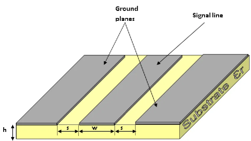
2.5 Coplanar Waveguide ... 66
Chapter 3: Microwave Filter ... 68
3.1 Introduction ... 68
3.2 Filters Based on Frequency Response ... 68
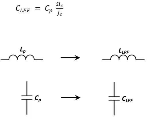
3.2.1 Lowpass Filter ... 68
3.2.2 Highpass Filter ... 70
3.2.3 Bandpass Filter ... 72
3.2.4 Bandstop Filter ... 74
3.3 Filters Based on Transfer Function ... 77
3.3.1 Butterworth Filter ... 78
3.3.2 Chebyshev Filter ... 79
3.3.3 Elliptic Filter ... 80
3.4 Filter Design Methods ... 80
3.4.1 Image Parameter Method ... 81
3.4.2 Insertion Loss Method ... 82
3.5 Immittance Inverters ... 83
3.5.1 Impedance Inverter ... 84
3.5.2 Admittance Inverter ... 86
3.6 SIW Bandpass Filter Design ... 89
3.6.1 Circuit Model Design and Simulation ... 91
3.6.2 SIW Design and Simulation ... 96
3.6.3 Fabrication and Measurement ... 102
3.6.4 Discussion ... 105
Chapter 4: Diplexer Circuit Analysis and Design ... 108
4.1 Introduction ... 108
4.2 Circuit Model Design ... 109
4.3 Circuit Model Coupling Arrangement ... 113
4.4 Circuit Model Simulation and Results ... 116
4.5 Conclusion ... 120
Chapter 5: Microstrip Diplexer Design ... 121
5.1 Introduction ... 121
5.2 Microstrip Square Open-Loop Resonator ... 121
5.3 Coupling Coefficient Extraction ... 124
v
5.5 Layout and Simulation ... 127
5.6 Fabrication and Measurement ... 130
5.7 Conclusion ... 133
Chapter 6: SIW Diplexer Design ... 135
6.1 Introduction ... 135
6.2 SIW Cavity ... 135
6.3 Coupling Coefficient Extraction ... 137
6.4 External Quality Factor Extraction ... 139
6.5 Layout and Simulation ... 141
6.6 Fabrication and Measurement ... 146
6.7 Conclusion ... 148
Chapter 7: Conclusion and Future Work ... 150
7.1 Conclusion ... 150
7.2 Future Work ... 152
List of Publications ... 153
vi
List of Figures
Figure 1.1: Radio frequency and microwave spectrums (Hong and
Lancaster, 2001). ... 2
Figure 1.2: RF front end of a cellular base station (Hunter et al., 2002). ... 4
Figure 1.3: 10-pole diplexer coupling scheme. (a) Conventional topology. (b) Common resonator topology. (c) Proposed topology. ... 10
Figure 1.4: Conventional diplexer architecture. ... 15
Figure 1.5: 12-pole manifold diplexer schematic (Skaik and AbuHussain, 2013). ... 17
Figure 1.6: A diplexer formed with filters and a circulator (He et al., 2012). . 19
Figure 1.7: Y-junction diplexer schematic (Shimonov et al., 2010). ... 20
Figure 1.8: 2n-pole T-junction diplexer schematic (Tsai et al., 2013). ... 21
Figure 1.9: Common resonator diplexer architecture. ... 23
Figure 2.1: Hollow rectangular waveguide geometry. ... 43
Figure 2.2: Microstrip line geometry (Hong and Lancaster, 2001). ... 44
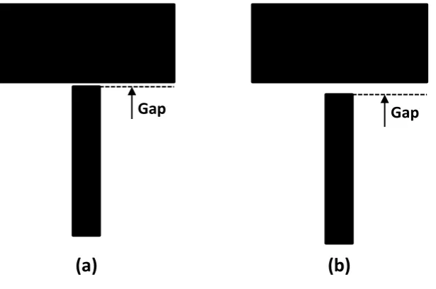
Figure 2.3: Microstrip patch resonators. (a) With strong coupling due to the narrow gap. (b) With weak coupling due to wide gap. ... 51
Figure 2.4: Microstrip quasi-lumped-element resonator. ... 52
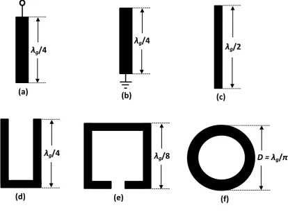
Figure 2.5: Some typical microstrip distributed-line resonators. (a) wavelength resonator for shunt-series resonance. (b) Quarter-wavelength resonator for shunt-parallel resonance. (c) Half-wavelength resonator. (d) Hair-pin resonator. (e) Square open-loop resonator. (f) Ring resonator. (Hong and Lancaster, 2001). ... 53
vii
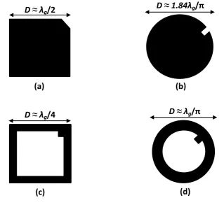
Figure 2.7: Some typical microstrip dual-mode resonators. (a) Square patch. (b) Circular disk. (c) Square loop. (d) Circular ring. (Hong and
Lancaster, 2001). ... 56
Figure 2.8: Substrate integrated waveguide evolution. (a) Air-filled waveguide. (b) Dielectric-filled waveguide. (c) Substrate integrated waveguide. ... 58
Figure 2.9: Physical geometry of the substrate integrated waveguide cavity. ... 59
Figure 2.10: TE1,0 mode surface current distribution of a rectangular waveguide with vias (or slots) on the narrow side walls (Xu and Wu, 2005). ... 61
Figure 2.11: Coplanar waveguide geometry. ... 67
Figure 3.1: Lowpass filter characteristic. ... 69
Figure 3.2: Normalised lowpass prototype to practical lowpass element transformation. ... 70
Figure 3.3: Highpass filter characteristic. ... 71
Figure 3.4: Normalised lowpass prototype to highpass element transformation. ... 72
Figure 3.5: Bandpass filter characteristic. ... 73
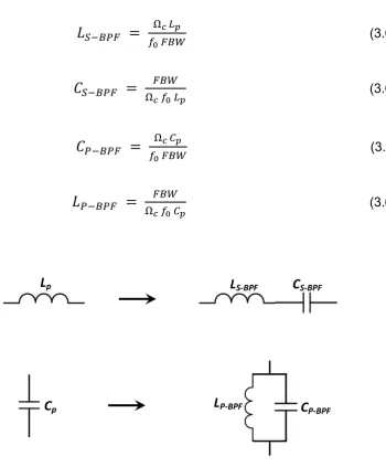
Figure 3.6: Normalised lowpass prototype to bandpass element transformation. ... 74
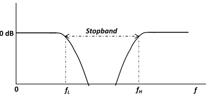
Figure 3.7: Bandstop filter characteristic. ... 75
Figure 3.8: Normalised lowpass prototype to bandstop element transformation. ... 77
Figure 3.9: Butterworth (maximally flat) lowpass filter response. ... 78
Figure 3.10: Chebyshev lowpass filter response. ... 79
Figure 3.11: Elliptic lowpass filter response. ... 80
viii
Figure 3.13: The stages of filter design by insertion loss method. ... 83
Figure 3.14: Ideal Impedance inverter (K-inverter) network. ... 84
Figure 3.15: Reactive circuit elements modelling of impedance inverter. (a) K-inverter to inductor-only network. (b) K-K-inverter to capacitor-only network. (Matthaei et al.,1980; Hong and Lancaster, 2001). ... 86
Figure 3.16: Impedance inverter used to convert a shunt capacitance into an equivalent circuit with series inductance (Hong and Lancaster, 2001). ... 86
Figure 3.17: Ideal admittance inverter (J-inverter) network. ... 87
Figure 3.18: Reactive circuit elements modelling of admittance inverter. (a) J-inverter to inductor-only network. (b) J-J-inverter to capacitor-only network. (Matthaei et al.,1980; Hong and Lancaster, 2001). ... 88
Figure 3.19: Admittance inverter used to convert a series inductance into an equivalent circuit with shunt capacitance (Hong and Lancaster, 2001). ... 89
Figure 3.20: Standard 3-pole (third order) normalised lowpass prototype filter (Yeo and Nwajana, 2013). ... 91
Figure 3.21: Normalised lowpass prototype filter with admittance inverters and shunt-only components (Yeo and Nwajana, 2013). ... 92
Figure 3.22: Chebyshev bandpass filter circuit model with identical parallel LC resonators and admittance inverters (Yeo and Nwajana, 2013). 93
Figure 3.23: Bandpass filter circuit model with J-inverters modelled as pi-network of capacitors. ... 94
Figure 3.24: Simulation responses of the bandpass filter circuit model. ... 95
Figure 3.25: Passband ripples of the Chebyshev bandpass filter circuit model. 95
Figure 3.26: Simulated coupling coefficient of a pair of substrate integrated waveguide cavities (Nwajana et al., 2017). ... 98
Figure 3.27: Microstrip-CPW-SIW input/output coupling structure for
ix
Figure 3.28: Diagram for extracting external Q-factor, Qext. (a) Variation of
Qext, with length, a, at b = 8.13 mm. (b) Variation of Qext, with
length, b, at a = 0.7 mm (Nwajana et al., 2017). ... 100
Figure 3.29: 3-pole (third order) bandpass filter coupling structure (Qext1 =
Qext2 = 21.21). ... 100
Figure 3.30: Layout of the 3-pole (third order) substrate integrated waveguide bandpass filter on a 1.27 mm thick substrate with a relative permittivity of 10.8 (Nwajana et al., 2017). ... 101
Figure 3.31: Full-wave simulation performances of the 3-pole (third order) substrate integrated waveguide bandpass filter. ... 102
Figure 3.32: Photograph of the fabricated 3-pole substrate integrated waveguide bandpass filter. (a) Top view. (b) Bottom view.
(Nwajana et al., 2017). ... 103
Figure 3.33: Measurement responses of the 3-pole (third order) substrate integrated waveguide bandpass filter. ... 103
Figure 3.34: Comparison of the measured and full-wave simulated 3-pole (third order) bandpass filter responses. ... 104
Figure 3.35: 3-pole substrate integrated waveguide filter simulated with circular, 10-sided polygon, and 4-sided polygon as metallic posts. ... 107
Figure 3.36: Graph of centre frequency against number of sides on the polygon used as metallic posts during the 3-pole SIW filter EM simulation. ... 107
Figure 4.1: Diplexer circuit arrangements. (a) With a non-resonant external T-junction. (b) With a non-resonant external common resonator. (c) Without any non-resonant external junction (Nwajana and Yeo, 2016). ... 109
Figure 4.2: Coupling arrangements for the 5th order (5-pole) Chebyshev
bandpass filters with the theoretical / calculated coupling
coefficients and external quality factor parameters indicated. (a) Tx channel. (b) Rx channel. ... 111
Figure 4.3: Coupling arrangement for the 10th order (10-pole) Chebyshev
x
Figure 4.4: Type-I. (a) Coupling arrangement. (b) Simulation responses. .. 114
Figure 4.5: Type-II. (a) Coupling arrangement. (b) Simulation responses. . 114
Figure 4.6: Type-III. (a) Coupling arrangement. (b) Simulation responses. 115
Figure 4.7: Type-IV. (a) Coupling arrangement. (b) Simulation responses.115
Figure 4.8: Proposed diplexer circuit model with the theoretical / calculated coupling coefficients and external quality factor values indicated. ... 117
Figure 4.9: Proposed diplexer circuit model with identical LC resonators and admittance inverters (Nwajana and Yeo, 2016). ... 118
Figure 4.10: Diplexer circuit model with admittance inverters (or J-inverters) modelled as pi-network of capacitors. ... 119
Figure 4.11: ADS simulation results of the proposed diplexer circuit model (Nwajana and Yeo, 2016). ... 120
Figure 5.1: Microstrip square open-loop resonator structure. ... 121
Figure 5.2: Microstrip square open-loop resonator. (a) Uncoupled. (b)
Electric coupling. (c) Magnetic coupling. (d) Mix coupling. ... 122
Figure 5.3: Microstrip square open-loop resonator dimensions. (a) Transmit band dimension. (b) Energy distributor dimension. (c) Receive band dimension. (Nwajana and Yeo, 2016). ... 123
Figure 5.4: Full-wave simulation layout and responses for the Tx, the Rx, and the ED resonators at their respective fundamental resonant frequencies. ... 124
Figure 5.5: Coupling coefficient extraction technique using the microstrip resonators. (a) Tx & Tx and Rx & Rx couplings. (b) ED & ED coupling. (c) Tx & ED and Rx & ED couplings. (Nwajana and Yeo, 2016). ... 124
Figure 5.6: External quality factor extraction technique. (Nwajana and Yeo, 2016). ... 127
Figure 5.7: 10-pole diplexer layout with physical dimensions indicated (S1 =
xi
S6 = 1.65 mm, S7 = 1.95 mm, S8 = 2.0 mm, S9 = 1.45 mm, t1 =
1.45 mm, t2 = 1.35 mm). (Nwajana and Yeo, 2016). ... 128
Figure 5.8: 10-pole (10th order) microstrip microwave diplexer layout on a
1.27 mm thick substrate with a dielectric constant of 10.8. ... 128
Figure 5.9: Comparison of the transmit and the receive bands responses of the microstrip diplexer layout and the circuit model of Chapter 4 operating in an ideal state (Nwajana and Yeo, 2016). ... 130
Figure 5.10: Simulation results of the microstrip diplexer with conductor and dielectric losses introduced into the system. ... 130
Figure 5.11: A picture of the fabricated 10-pole microstrip diplexer. (Nwajana and Yeo, 2016). ... 131
Figure 5.12: Measurement results of the 10-pole (10th order) microstrip
diplexer. ... 132
Figure 5.13: Comparison of the full-wave electromagnetic loss simulation results and the measurement results of the 10-pole microstrip diplexer. ... 133
Figure 6.1: Full-wave simulation layout and the results for the Tx, the Rx, and the ED substrate integrated waveguide cavities at their
respective fundamental resonant frequencies. ... 137
Figure 6.2: Coupling coefficient extraction technique using the substrate integrated waveguide cavities. (a) Tx & ED and Rx & ED couplings. (b) Tx & Tx and Rx & Rx couplings. (c) ED & ED coupling. ... 138
Figure 6.3: External quality factor extraction technique for the ED
component. ... 140
Figure 6.4: Simulation response of the transition from coplanar waveguide to substrate integrated waveguide (i.e. CPW – to – SIW) using a 90o bend. ... 141
Figure 6.5: 10-pole substrate integrated waveguide diplexer layout indicating physical dimensions, on a 1.27 mm thick RT/Duroid 6010LM substrate with a dielectric constant of 10.8. ... 142
xii
Figure 6.7: FEM padding editor window indicating the settings used for the substrate integrated waveguide diplexer full-wave finite-element method simulations. ... 145
Figure 6.8: Photograph of the fabricated 10-pole substrate integrated
waveguide diplexer. (a) Top view. (b) Bottom view. ... 146
Figure 6.9: Measurement results of the 10-pole (10th order) substrate
integrated waveguide diplexer. ... 147
xiii
List of Tables
Table 3.1: Chebyshev lowpass prototype filter parameters. ... 91
Table 3.2: 3rd order (3-pole) Chebyshev bandpass filter design parameters.
... 94
Table 3.3: Physical dimensions and numerical parameters of the substrate integrated waveguide bandpass filter (Nwajana et al., 2017). . 101
Table 4.1: 5th order (5-pole) Chebyshev bandpass filter design parameters.
... 110
Table 4.2: 5th order (5-pole) Chebyshev bandpass filter coupling coefficient
and external quality factor values. ... 111
Table 4.3: 10th order (10-pole) Chebyshev dual-band bandpass filter design
parameters. ... 112
Table 4.4: 10th order (10-pole) Chebyshev dual-band bandpass filter
coupling coefficient and external quality factor values. ... 112
Table 5.1: Simulated separation distance values for the proposed diplexer couplings. ... 126
Table 6.1: Physical design parameters for the substrate integrated
waveguide diplexer component filters cavities. ... 136
Table 6.2: Physical dimensions of the proposed 10-pole substrate
xiv
List of Symbols and Abbreviations
2D Two-Dimensional
3D Three-Dimensional
AC Alternating Current
ADS Advanced Design System
BPF Band-Pass Filter
BSF Band-Stop Filter
C Capacitance of a capacitor
C0 Speed of light in free space
CAD Computer-Aided Design
CPW Co-Planar Waveguide
CR Common Resonator
d Diameter of metallic post (or diameter of via)
dB Decibel
DBF Dual-band Bandpass Filter
DC Direct Current
D-CRLH-MTM Dual Composite Right-Left Handed Metamaterial
E Electric
ED Energy Distributor
xv
EMPro Electro-Magnetic Professional
f Frequency
f0 Fundamental resonant frequency (or cut-off frequency)
FBW Fractional Band-Width
FEM Finite Element Method
fH Higher frequency boundary
fL Lower frequency boundary
fr Resonant frequency
FSIW Folded Substrate Integrated Waveguide
GCPW Grounded Co-Planar Waveguide
GHz Giga-Hertz
GIPD Glass-based Integrated Passive Devices
h Substrate thickness
HMSIW Half-Mode Substrate Integrated Waveguide
HPF High-Pass Filter
HTS High-Temperature Semiconductor
IEEE Institute of Electrical and Electronic Engineers
IL Insertion Loss
J-inverter Admittance inverter
xvi
Ka Asynchronous coupling coefficient
K-inverter Impedance inverter
Ks Synchronous coupling coefficient
L Inductance of an inductor
l Length
LCP Liquid Crystal Polymers
leff Effective length
LKPF Leiterplatten-Kopierfräsen
LPF Low-Pass Filter
LTCC Low-Temperature Co-fired Ceramics
M Magnetic
MatLab Mathematical Laboratory
MEMS Micro-Electro-Mechanic Systems
MHz Mega-Hertz
MMT Mode Matching Technique
mm-Wave Millimetre Wave
nH Nano-Henry
p Pitch (or distance between two metallic posts)
PCB Printed Circuit Board
xvii
PIM Passive Inter-Modulation
Pr Passband ripple
Q Quality factor (or unloaded quality factor)
Qext External quality factor
Q-Factor Quality Factor
QL Loaded quality factor
R Resistance of a resistor
RF Radio Frequency
RL Return Loss
Rs Skin Resistance
Rx Receive
s Spacing (or separation distance)
S11 Simulation / measurement return loss
S21 Simulation / measurement transmit band insertion loss
S31 Simulation / measurement receive band insertion loss
S32 Simulation / measurement isolation between transmit and
receive bands
SIR Stepped Impedance Resonator
SIW Substrate Integrated Waveguide
SLR Slot-Line Resonator
xviii
SOLR Square Open-Loop Resonator
t Tapping distance (also, signal line thickness)
T Transfer function
tan δ Loss tangent
TE Transverse Electric
TEM Transverse Electro-Magnetic
TL Transmission Line
TM Transverse Magnetic
Tx Transmit
V Voltage
w Width
weff Effective width
YL Load admittance
Ys Source admittance
Z Impedance
Z0 Characteristic impedance
ZL Load impedance
Zs Source impedance
αc Conductor loss mechanism
xix
αr Radiation loss mechanism
εeff Effective permittivity (or effective dielectric constant)
εr Relative permittivity (or relative dielectric constant)
λ Wavelength
λg Guided wavelength
μr Relative permeability
σc Conductivity of copper
ω Angular frequency
Ω Low-pass prototype frequency domain
ωc Cut-off angular frequency
Ωc Low-pass prototype cut-off frequency
xx
Acknowledgements
I would like to thank my director of studies (i.e. my first supervisor), Dr Kenneth
S. K. Yeo for his wonderful guidance and support throughout the period of my
PhD research. He did not only act as my lead supervisor but also went extra miles
in ensuring that my work was fabricated, in the absence of the workshop
technicians. I would also like to thank my second supervisor, Dr Wada W. M.
Hosny for his advice at the beginning of my research journey. His feedback during
my transfer from MPhil to PhD was very helpful.
My sincere gratitude also goes to Professor Allan J. Brimicombe who taught me
on the research method module in the first year of my research. His guidance
and support helped me through the process of registering my PhD research topic
with the UEL graduate school.
Finally, this acknowledgment will be incomplete without the mention of my
research colleague, Amadu, who has been a member of my research team since
the start of this project in 2013. He is a wonderful gentleman to have as a team
xxi
Dedication
This thesis is dedicated to my lovely wife, Mrs Amaka Calista Nwajana (a.k.a.
AsaFano) who shouldered most of the responsibilities of taking care of our
wonderful kids (Muna & Ife) while I accomplish this profound task. I also like to
welcome Onyie to our lovely family. This research work is for you as you
decided to join the family in this particular month that I am submitting my thesis.
1
Chapter 1: Introduction
1.1 Background
The need to miniaturise in size, as well as reduce the design complexity of
microwave and millimetre-wave components, circuits and devices; while
maintaining (or even improving on) the quality of such components, circuits and
devices has recently drawn a lot of attention from researchers in this research
field. The term microwave, in this context, is used to describe electromagnetic
(EM) waves with frequencies beginning from 300 MHz and ending at 300GHz.
The microwave frequency range (i.e. 300 MHz to 300 GHz) corresponds to the
free space wavelengths of 1 m to 1 mm as shown in Figure 1.1 (Hong and
Lancaster, 2001). EM waves with frequencies ranging from 30 GHz to 300 GHz
are also referred to as millimetre-waves as a result of their wavelengths being in
the millimeter range i.e. 1 mm to 10 mm. According to Hong and Lancaster
(2001), the radio frequency (RF) spectrum lies below the microwave frequency
spectrum. However, the boundary between the RF and microwave frequencies
is arbitrary and depends on the particular technology developed for the
exploitation of the given specific frequency range (Hong and Lancaster, 2001). It
is important to note that the frequency values in Figure 1.1 increase in the reverse
direction to the wavelength values. This is in agreement with Eqn. (1.1) where c0
is the speed of light in free space, f is the frequency, and λ is the wavelength.
𝑓 =
𝑐02
Figure 1.1: Radio frequency and microwave spectrums (Hong and Lancaster, 2001).
Microwave diplexer is a device that has attracted a lot of interest due to its ability
to allow two separate components to share one communication medium
(Nwajana and Yeo, 2016). The aforementioned advantage makes the diplexer a
cost effective and less bulky alternative to communicating through two separate
transmit and receive channels. Due to the vast applications of diplexers in
communication engineering, researchers have been coming up with novel and
better design methods to enable engineers cope with the ever increasing
demands of modern communication systems. The design of diplexers has always
presented the design engineers with ever growing stringent requirements such
as: selectivity, bands isolation, high performance, smaller size, lighter weight,
lower cost, etc. RF and microwave diplexers could be designed as lumped
elements or distributed elements circuits, but this will depend on requirements
and specifications. Diplexers may be achieved with different transmission line
techniques including: waveguide, slot-line, strip-line, coaxial line, micro-strip line,
coplanar waveguide (CPW), etc. Advancements in computer-aided design (CAD)
tools including full-wave electromagnetic (EM) and finite-element method (FEM)
simulators have revolutionised the diplexer design and characterisation process
Frequency
Wavelength 1 km 100 m 10 m 1 m 10 cm 10 mm 1 mm
3
(Hong and Lancaster, 2001). The popular fabrication technologies that has been
investigated and reported for modern day diplexers include: printed circuit board
(PCB) (Hao et al., 2005; Tang et al., 2007; Nwajana and Yeo, 2016),
micro-electro-mechanic systems (MEMS) also referred to as micromachining (Hill et al.,
2001; Reid et al., 2008; Skaik et al., 2011), high-temperature superconductors
(HTS) (Heng et al., 2013; Zheng et al., 2014; Zheng et al., 2015; Guan et al.,
2016), low temperature co-fired ceramics (LTCC) (Fritz and Wiesbeck, 2006; Kim
et al., 2010; Chu et al., 2011), liquid crystal polymers (LCP) (Govind et al., 2006;
Ashiq and Khanna, 2015), etc.
A diplexer is the simplest form of multiplexer that is widely used for either splitting
a frequency band into two bands of frequencies, or for combining two
sub-bands into one wide frequency band (Yun et al., 2005; Zhu et al., 2014). Diplexers
are popularly used in satellite communication systems to combine both the
transmit (Tx) and the receive (Rx) antennas on space crafts. This can reduce the
mass and volume of the space craft to a considerable amount, as only one
antenna is required to transmit and also receive signals (Yun et al., 2005). As a
frequency selective device, the diplexer connects two different networks with
different operating frequencies to a single port. Diplexers are commonly used in
Radio Frequency (RF) front end of cellular radio base stations to separate the Tx
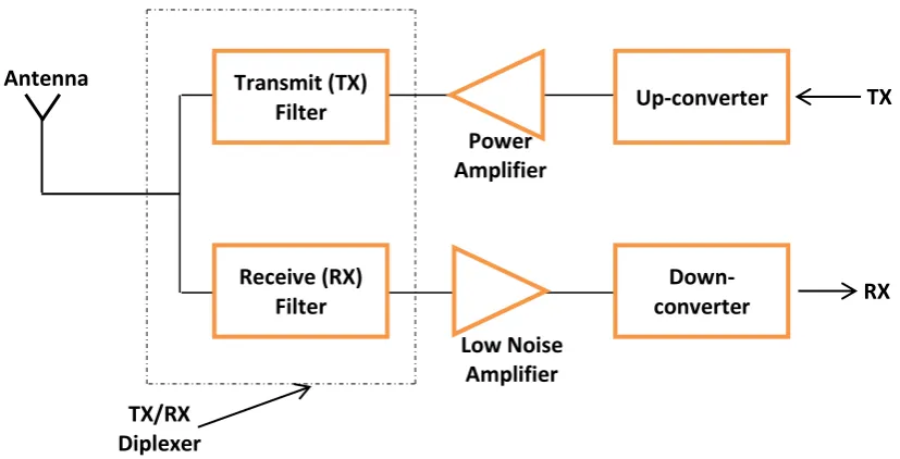
and the Rx bands as shown in Figure 1.2 (Hunter et al., 2002). The diplexer is an
important device in the entire system; it is made up of two channel filters and a
power splitter. The Tx / Rx diplexer shown in Figure 1.2 allows for the
simultaneous transmission and reception of signals through the single antenna.
The Tx filter is designed to have high power handling ability to enable it cope with
4
other hand, is only needed to handle very weak signals from the receiver.
Therefore, no power handling consideration is needed at the Rx channel. The
isolation between the Tx and the Rx bands is a design parameter that must be in
the forefront when the diplexer is being formed. This is because a poor isolation
between the transmit and the receive bands would mean that a large amount of
signal, could be deflecting towards the wrong direction during the diplexer
operation. In summary, microwave diplexers are three-port devices that typically
[image:25.595.119.533.303.514.2]operate over the frequency range of 300 MHz – 300 GHz.
Figure 1.2: RF front end of a cellular base station (Hunter et al., 2002).
The selectivity of the Tx and the Rx bands of diplexers is another very important
design criteria that should be put into consideration when designing a diplexer.
Several authors have proposed different methods for designing microwave
diplexers. The conventional approach to achieving a diplexer is to connect two
separately designed filters together using an external non-resonant energy
distribution connector. This connecting component could be: a T-junction (Liu et
TX/RX Diplexer Antenna
TX
Power Amplifier Transmit (TX)
Filter Up-converter
RX
Low Noise Amplifier Receive (RX)
Filter
5
al., 2013; Yiming and Xing, 2010), a Y-junction (Bastioli et al., 2009; Xu et al.,
2007), a circulator (Kodera and Caloz, 2010), a manifold (Heng et al., 2014;
Morini et al., 2015) or an out of band common resonator (Yang and Rebeiz, 2013;
Tantiviwat et al., 2013). The separate energy distribution connector used in the
conventional method of diplexer design had resulted to relatively complex and
larger size devices (Nwajana and Yeo, 2016). The complexity of the conventional
design approach is as a result of involving the external connecting component or
junction, which needs to be continuously adjusted and optimised before an
expected result could be realised. The large size problem of the conventional
design is as results of the fact that the separate junction component does not
contribute to the number of poles contained in the resulting diplexer transmit and
receive channels. This means that the external / separate junction has very little
or no contribution to the diplexer selectivity, but only there to split the channel and
hence, contributing slightly to the relatively larger size of the conventional
diplexer.
To overcome the drawbacks associated with the conventional diplexer design
method, the work reported in this thesis has successfully eliminated the need for
employing the external / separate junction connector in achieving a diplexer and
replacing it with resonators that contribute resonant poles to the diplexer
responses. This thesis report will show that the design complexity associated with
the conventional diplexer design approach, can be averted with a good mastery
of the basic principles associated with bandpass filter (BPF) design as reported
in Hong and Lancaster (2001), and the dual-band bandpass filter (DBF) design
as reported in Yeo and Nwajana (2013). By this novel method, design engineers
6
developing complex optimisation algorithms (Wang et al., 2012; Shang et al.,
2013) to achieve the same function. Also, considering the fact that the diplexer
reported in this thesis is formed by coupling a section of the Tx and the Rx
channel filters resonators, onto a section of the DBF resonators; a reduced sized
diplexer is achieved. The reason for the reduced size in the resulting diplexer is
because the DBF resonators contribute one resonant pole to the diplexer Tx
channel and one resonant pole to the diplexer Rx channel. Parts of the results
from this thesis have been published in Nwajana and Yeo (2016) and Nwajana
et al. (2017).
The diplexer design method proposed in this thesis involves cascading a section
of a dual-band bandpass filter, with a section of two bandpass filters. A dual-band
bandpass filter is a filter that passes two bands of frequencies while attenuating
frequencies outside the two bands (Deng et al., 2006; Nwajana and Yeo, 2016).
A bandpass filter, on the other hand, is a filter that passes frequencies within a
single band while rejecting all other frequencies outside the band. The pair of
DBF resonators reported here can be viewed as an energy distributor (ED) which
distributes energy towards the Tx and the Rx bands of the diplexer. The DBF
resonators serve as replacements to the external junction or connector used in
other diplexer design methods found in existing literature. The actual function of
the DBF resonators employed in this work is to establish the two pass-bands of
7
1.2 Motivation and Problem Statement
The increasing demand and high interest in size miniaturization, as well as
reduction in design complexity of microwave components, have motivated a lot
of researchers into seeking solutions and remedies to the ever growing
challenges. Microwave diplexer is one of the essential components in the RF front
end of most multi-service and multi-band communication systems and
sub-systems. This is because the presence of the diplexer reduces the number of
antennas required in a system (Deng et al., 2013). The RF front end of any
cellular base station is a very good example of a system that has highly benefitted
from the merits of achieving a diplexer with simple design and reduced size. The
diplexer present in the RF front end of a cellular base station makes it possible
for an input signal with two different frequencies, to split into two different signals
at the output ports. It also facilitates the combination of two different input signals
into one signal at the output port (Xiao et al., 2015).
The main motivation behind the research work reported in this thesis is to achieve
a diplexer where each resonator contributes a resonant pole to the diplexer
response for reduced size. This means that the proposed diplexer will not rely on
any external non-resonant device for energy distribution as is the case with most
diplexers design methods reported in literature. The proposed diplexer will also
be based on known mathematical formulations for bandpass filter and dual-band
bandpass filter designs for simplicity. Some authors have offered different design
techniques to achieving diplexers of reduced size but based on complex
polynomial evaluation. Skaik and Lancaster (2011) and Skaik et al. (2011)
8
optimisation. The optimisations of the coupling matrix reported in those papers
were based on the minimisation of cost functions that were evaluated in order to
derive the diplexers. This is an effective but complex way to achieve a diplexer
response, as a good mastery of the polynomial evaluation and reduction /
convergence technique is highly required. In a related research paper (Lin and
Yeh, 2015), a triplexer based on parallel coupled-line filters using T-shaped
short-circuited resonators was reported. The design was based on a connecting
junction and matching transmission lines. The design of a quad-channel diplexer
using stepped impedance resonators (SIRs) has also been researched and
presented (Wu et al., 2013). The quad-channel diplexer is made up of two pairs
of coupled SIRs with an impedance ratio that is greater than 1, and the
quarter-wavelength source / load coupling lines. The resonant modes of the SIRs were
simply determined by tuning their impedance ratio and length ratio. This facilitated
the implementation of bandpass filters with very close dual-passbands. The
source / load coupling lines were designed to correspond to the
quarter-wavelength at the centre frequency of the first passband at each output port. The
quad-channel diplexer configuration is a simple and relatively effective design
approach when compared to the conventional diplexer design technique. The
resultant diplexer is also of relatively small size as opposed to conventional
standard.
Wang and Xu (2012) reported a diplexer with relatively reduced size when
compared to the conventional diplexers. The design was based on the evaluation
of the characteristic polynomial functions and the optimisation of error functions
to achieve coupling. It employed a common resonator in place of the external
9
for energy distribution neither contribute a pole to the transmit band nor the
receive band of the resulting diplexer. This is evident in the diplexer response
curves presented in the paper (Wang and Xu, 2012). For example, the
10-resonator diplexer presented produced 5 poles on the transmit band and 4 poles
on the receive band, while the 7-resonator diplexer produced 3 poles on the
transmit band and another 3 poles on the receive band. The additional resonator
is an out of band resonator which is used for coupling the transmit and the receive
paths. Hence, the addition resonator used to split the bands in each case does
not contribute any pole to either bands of the diplexer but will take up additional
real estate of the design.
The diplexer reported in this thesis neither uses an external non-resonant junction
nor a common resonator for energy distribution. Instead, a pair of dual-band
bandpass filter (DBF) resonators were coupled onto the transmit (Tx) and the
receive (Rx) channel filters resonators to form the diplexer. This simply means
that the pair of DBF resonators replaces the first resonators of both the Tx and
the Rx channel filters. The coupling scheme for a 10-pole (10th order) diplexer is
10
Figure 1.3: 10-pole diplexer coupling scheme. (a) Conventional topology. (b) Common resonator topology. (c) Proposed topology.
The conventional (i.e. junction) diplexer is represented in Figure 1.3 (a), while the
common resonator diplexer and the proposed diplexer are shown in Figure 1.3
(b) and Figure 1.3 (c), respectively. D1 and D1’ in Figure 1.3 (c) are the pair of
dual-band bandpass filter resonators; T1, T2, T3, T4, T5 and R1, R2, R3, R4, R5
are the Tx and the Rx channel filters resonators, respectively. The external
Port 1
T2
T1 T3 T4 T5
R2
R1 R3 R4 R5
Port 2
Port 3 Junction
(a)
Port 1
T2
T1 T3 T4 T5
R2
R1 R3 R4 R5
Port 2
Port 3 Common Resonator
(b)
T3
T2 T4 T5 Port 2
R3
R2 R4 R5 Port 3
Port 1 D1 D1’
11
junction indicated in Figure 1.3 (a) could be a T-junction (Chen et al., 2014; Shi
et al., 2011), a Y-junction (Shimonov et al., 2010), a circulator (Saavedra, 2008)
or a manifold (Taroncher et al., 2006). A diplexer based on a coupling scheme
similar to that of the common resonator shown in Figure 1.3 (b) was proposed in
Chen et al. (2006).
1.3 Research Method
The most widely employed method when it comes to the design of RF and
microwave diplexers is to use two separately designed bandpass filters, having
distinct frequencies, with a three-port impedance matching network. The
combining network (i.e. the impedance matching network) is normally aimed at
producing good transmission in one passband and exhibiting high impedance in
the other passband, in order to achieve the necessary channel isolation (Wu et
al., 2015). The reality is that designing a matching network that can produce a
very good transmission in one passband and a good attenuation in the other
passband is a very challenging feat to achieve (Guan et al., 2014). Numerous
examples abound in literature were researchers have successfully achieved
diplexers using a three-port matching network. T-junctions (Zhang et al., 2010;
Hung et al., 2010) are the most popular matching networks used in diplexer
design. Other types of junctions that have been employed in achieving diplexers
include: the manifold (Rhodes and Levy, 1979; Packiaraj et al., 2005), the
Y-junction (King et al., 2011; Harfoush et al., 2009), and the circulator (He et al.,
2012). A common resonator (Guan et al., 2016; Chen et al., 2006) has also been
used in place of the matching network to successfully achieve multiport devices
12
The method of diplexer design proposed in this thesis involves cascading a
section of a dual-band bandpass filter (DBF), with sections of two separately
designed bandpass filters (BPFs) as shown in Figure 1.3 (c). D1 and D1’ are the
first pair of dual-band resonators obtained by separately designing a DBF, whose
fractional bandwidth (FBW) is equal to the combined FBWs of the two BPFs that
would form the transmit (Tx) and the receive (Rx) channels of the proposed
diplexer. The main function of the pair of dual-band bandpass filter resonators
present in the proposed diplexer is to establish the two pass-bands of the
diplexer. Like the external junctions used in the conventional diplexer design
approach, the dual-band bandpass resonators are responsible for distributing
energy towards the Tx and the Rx bands of the diplexer. Unlike the external
junctions that do not contribute to the number of poles present in the resultant
diplexers, the dual-band bandpass filter resonators do contribute to the number
of poles by physically replacing one resonator from the Tx channel and one
resonator from the Rx channel as shown in Figure 1.3 (c). This explains why the
physical size of the proposed diplexer is relatively smaller when compared to that
of the conventional diplexer.
The circuit model of the proposed diplexer was simulated using the Keysight
Advanced Design System (ADS) circuit simulator, while the microstrip layout
simulation was achieved using the Keysight ADS momentum simulator. The
electromagnetic (EM) simulation of the SIW layout of the proposed diplexer was
based on the finite-element method (FEM) of the Keysight electromagnetic
13
professional circuit, EM or even FEM simulators could be used to achieve results
similar to those presented in this thesis. The microstrip diplexer fabrication was
based on the printed circuit board (PCB) milling process, while the SIW diplexer
was fabricated using the PCB micro-milling process based on the
Leiterplatten-Kopierfrasen (LKPF) Protomat C60.
1.4 Literature Review
A diplexer is the simplest form of multiplexer. It is a three port (3-port) frequency
distribution device mostly utilised in communication networks. Microwave
diplexers are widely used in splitting input signals from a single port, into two
communication channels operating at different frequencies. They can also be
used to combine two separate communication channels into a single combined
signal for transmission via a shared antenna. The transmitter and the receiver of
diplexers are designed to operate at different frequency bands and are duplexed
to the transceiver diplexer (Chen et al., 2011). It is important to note the clear
difference between a diplexer and a duplexer. Though both devices (i.e. diplexer
and duplexer) have similar design procedures, the transmit channel of a duplexer
suffer from power handling issues. Hence, this must be considered when
duplexers are been designed. The transmit and the receive bands terminologies
repeatedly referred to throughout this thesis are for the two channels of the
diplexer. Therefore, no power handling issues have been considered in this
thesis. In designing a microwave diplexer, an accurate computer aided design
(CAD) is required in order to avoid the over reliance on turning screws or any
other adjusting component which actually limits the maximum transmittable
14 1.4.1 Diplexers Based on Design Approach
Various approaches to the design of diplexers have been reported in literature.
The most vastly reported approach to designing diplexers is the conventional
method which involves combining two bandpass filters (BPFs) with a three-port
impedance matching network (Chan, 2015) such as a manifold (Guglielmi, 1993;
Ye and Mansour, 1994), a circulator (Saavedra, 2008; Kodera and Caloz, 2010),
a T-junction (Thirupathaiah et al., 2014; Kordiboroujeni et al., 2014), or a
Y-junction (Bastioli et al., 2009, Wu and Meng, 2007). Another approach that has
been recently reported is the common resonator method, which involves
replacing the three-port impedance matching network of the conventional method
with a common resonator. The synthesis of coupled resonator diplexers based
on linear frequency transformation and optimisation have also been reported
(Wang et al., 2012; Macchiarella and Tamiazzo, 2006). This approach is based
on the evaluation of suitable characteristic polynomials of the diplexer.
The traditional or conventional approach to achieving a diplexer is to combine two
separately designed bandpass filters (BPFs) with a three-port impedance
matching network as shown in Figure 1.4. The two BPFs are distinctly designed
to operate at different frequencies that correspond to the frequencies of the
transmit (Tx) and the receive (Rx) bands of the target diplexer. The combining
network, which in this case is the 3-port impedance matching network, is normally
designed to produce good transmission in one passband and exhibit high
impedance in the other passband (Wu et al., 2015). This stringent design
condition of the 3-port impedance matching network is to facilitate the
15
Guan et al. (2014), designing a matching network that can produce a good
transmission in one passband and a good attenuation in the other passband is a
very challenging feat to achieve. The performance of a conventional diplexer will
highly depend on the channel filters, as well as the 3-port matching network
(Chan et al., 2015). This is because the overall losses experienced in the diplexer
are due to the sum of all the individual losses contributed by the channel filters
and the combining network.
Figure 1.4: Conventional diplexer architecture.
The 3-port matching network shown in Figure 1.4 could be a manifold, a
circulator, a Y-junction or a T-junction. In addition to contributing to the size and
complexity of a diplexer, each type of matching network has its peculiar
disadvantage. For example, tuning of diplexers / multiplexers designed with a
manifold as the connecting device can be time-consuming and expensive. Such
diplexers are also not open to flexible frequency plan; meaning that changes in
any channel frequency will require a totally new diplexer design (Cameron and
Yu, 2007). On the other hand, diplexers employing circulators as the connecting
device suffer from extra loss per trip as signals must pass in succession through
the circulator. According to Cameron and Yu (2007), low-loss, high-power ferrite
circulators are expensive. Circulators are also prone to higher level of passive
Rx Filter Tx Filter 3-port
Matching Network Port 1
Port 1
16
intermodulation (PIM) products when compared to T- and Y- junctions and
manifolds. Various authors have reported different diplexers/multiplexers
achieved by means of employing each and every one of the four types of 3-port
matching network highlighted in this sub-section.
Rhodes and Levy (1979) reported a multiplexer with immittance compensation.
The involvement of the immittance compensation was done in such a way that
not only preserved the canonic form of the multiplexer network, but also assisted
in the physical construction by spacing the channel filters along the manifold. In
another research paper (Guglielmi, 1993), the computer aided design (CAD)
procedure for the manufacture of a class of manifold diplexers was described.
This approach was based on filters implemented with thick inductive windows in
rectangular waveguide. A study by Packiaraj et al. (2005) reported a manifold
cavity diplexer based on tapped line interdigital filters topology. The work made
provision for tuning screws at the end of each resonator to carter for post
fabrication tuning. In a different study, the authors combined finite element
electromagnetic based simulators with space mapping optimisation to produce
manifold-coupled multiplexers, with dielectric resonator loaded filters (Ismail et
al., 2012). A novel X-band diplexer based on overmoded circular waveguides for
high-power microwaves was proposed by Li et al. (2013). The research finding
relied on mode-matching techniques and numerical optimisation to achieve
results. A radial waveguide structure with six rectangular ports was used as the
duplexing manifold (Li et al., 2013). The schematic diagram of a 12-pole manifold
17
Figure 1.5: 12-pole manifold diplexer schematic (Skaik and AbuHussain, 2013).
In another investigation, a manifold-coupled narrowband superconducting
quadruplexer with high isolation was reported (Heng et al., 2014). The work
employed a binary matching network in order to minimise the undesired
interactions amongst the four channels of the quadruplexer. Carceller et al.
(2015) reported on manifold-coupled multiplexers with compact wideband. The
method used was based on the sequential connection of filters to the manifold,
and then making some adjustments at the point of interconnection. The filters
were attached to the manifold without the use of stubs, thereby, minimising the
effect of spurious resonance (Carceller et al., 2015). The efficient design of
waveguide manifold multiplexers based on low-order electromagnetic (EM)
distributed models (Cogollos et al., 2015) has also been reported. The main
requirement for the design is that all channel filters and other design elements
must be successfully represented by means of distributed models. Even though
manifold diplexers / multiplexers are capable of realising optimum performance,
both in terms of absolute insertion loss and amplitude and group delay response
18
size, complex design, time consuming and expensive tuning, and are not
responsive to a flexible frequency plan. This means that a change of a channel
frequency will require a new diplexer / multiplexer design.
Circulators are another group of traditional or conventional impedance matching
network devices that have been employed in the design of microwave diplexers.
When compared to manifolds, diplexers achieved using circulators are simple to
tune as channel filters do not interact. They are also responsive to flexible
frequency plan (Cameron and Yi, 2007). Like the manifolds, however, circulators
contribute to the large size of resultant diplexers / multiplexers. They have higher
level of passive intermodulation (PIM) products when compared to manifolds or
even the T- and the Y- junctions. It is also expensive to obtain low-loss,
high-power ferrite circulators. They have a peculiar disadvantage of making signals
pass in succession through the circulator, thereby, incurring extra loss per trip
(Cameron and Yi, 2007). A number of research papers have, in the past decade,
reported diplexers based on circulators. Saavedra (2008) proposed a diplexer
employing a circulator and interchangeable filters. The microwave diplexer
employed a passive or active 3-port clockwise circulator device. ‘The use of a
circulator in place of a manifold structure in the diplexer means that the filters can
be tuned or even exchanged without the need to modify the manifold’ (Saavedra,
2008). In another research paper, a SIW circulator was used in the design of a
novel compact Ka-band high-rejection diplexer (He et al., 2012). The SIW
circulator employed in the design uses inductive windows to increase bandwidth.
The entire design, including both channel filters and circulator as shown in Figure
19
[image:40.595.239.395.80.235.2]
Figure 1.6: A diplexer formed with filters and a circulator (He et al., 2012).
Diplexers achieved by employing Y- and T- junctions are very similar in their
design and operation. Like every other external matching network, the Y- and the
T- junctions contribute to the size and complexity of the resultant diplexer. When
compared to circulators, the Y- and the T- junctions exhibit low level of PIM
products. Microwave diplexers formed with a Y- or a T- junction are simple to tune
as there exist no interaction between channel filters. They are also amenable to
modular concept, i.e. any change of a channel frequency may not necessarily
require a new diplexer design.
The Y-junction has been reported in a number of published works found in
literature. Xu et al. (2007) used a dual-mode rectangular stripline ring resonator
to design two separate filters and then used a Y-junction feed-line to connect the
two filters to form a diplexer circuit. Another research paper presented a diplexer
designed and implemented in the X-band frequency (Harfoush et al., 2009). The
two channels of the diplexer were designed using a waveguide Y-junction to
20
(2009) proposed a resonant junction for compact waveguide diplexers. The
Y-junction employed in the design contained an elliptic ridge which served as a
common dual-mode resonator for both the transmit (Tx) and the receive (Rx)
channels of the diplexer. A diplexer which is formed by a combination of two
electric plane (E-plane) filters and a magnetic plane (H-plane) Y-junction splitter
has been reported (Shimonov et al., 2010). The design was based on the mode
matching technique (MMT) and used the diplexer schematic shown in Figure 1.7.
In a study by King et al. (2011), a microstrip diplexer using step impedance
resonator (SIR) with folded hairpin structure was reported. The diplexer was
achieved by separately designing two distinct bandpass filters (BPFs) and then
connecting them with a Y-junction.
Figure 1.7: Y-junction diplexer schematic (Shimonov et al., 2010).
T-junctions are by far the most widely used 3-port impedance matching network
employed in the design of microwave diplexers. This is a fact based on published
works available in literature. The schematic diagram of a 2n-pole T-junction
diplexer is given in Figure 1.8 (Tsai et al., 2013). Different authors have employed
21
design of a diplexer based on dual composite right-left handed metamaterial
(D-CRLH-MTM) have been reported (Mansour et al., 2014). The design was formed
by using a T-junction to combine two notch filters having different stop bands. In
a different study, Chen et al. (2015) proposed a wide-band T-junction and
bifurcated SIW diplexer. The T-junction employed in their work was designed to
have short arms. This is to ensure that junction resonance in the wide-band
frequencies are kept at the barest minimum (Chen et al., 2015).
Figure 1.8: 2n-pole T-junction diplexer schematic (Tsai et al., 2013).
Another research paper reported a T-junction SIW diplexer based on circular
triplet combline filter sections (Sirci et al., 2015). The design placed the
transmission zeros of the diplexer below and above the passband. Positive and
negative couplings were conveniently provided to facilitate the control of the
location of each transmission zero in the diplexer responses. Rezaee et al. (2015)
proposed a V-band diplexer based on the groove gap waveguide technology. The
diplexer was formed by combining two channel filters with an H-plane T-junction.
The major advantage of the groove gap waveguide diplexer over the traditional
waveguide diplexer is that there is no need for an electrical contact between the
top and the bottom metal plate. This is vital as it provides an opportunity for the
22
isolation employing multi-order resonances (Wang et al., 2015) and a switchable
diplexer design employing switchable bandpass filters (Xu, 2016) have both been
reported. Both reports used the T-junction as the three-port matching network for
energy distribution. A compact broadband waveguide diplexer that covers the
Ku-band transmit and receive channels has also been proposed (Teberio et al.,
2016). The diplexer was formed by combining a T-junction with a compact
Ku-band, high-power lowpass and bandpass filters based on inductive irises. In
another interesting research paper by Lee et al. (2016), a balance quad-band
diplexer with wide common mode suppression and high differential-mode
isolation was proposed. The 6-port balanced diplexer was achieved by
connecting two dual-band bandpass filters through two stepped-impedance
Resonators (SIRs) inserted T-junctions (Lee et al., 2016). The common
disadvantages of all T- junction based diplexers are their increased size and
design complexity.
A more recent approach to the design of microwave diplexer is to replace the
three-port matching network of the traditional / conventional diplexer with a
common resonator (CR) as shown in Figure 1.9. Though this recent method has
proved effective in achieving diplexers of relatively small size when compared to
the conventional approach, more size reduction can still be achieved using the
approach proposed in this thesis. The common resonator method of diplexer
design involves connecting two separately designed filters by means of a CR as
the connecting device. Like the conventional diplexer, the performance of a CR
diplexer will depend on the two channel filters and common resonator
23
to the individual losses contributed by each channel filter and the common
resonator.
Figure 1.9: Common resonator diplexer architecture.
A number of research papers have, in the past decade, reported diplexers
achieved based on the common resonator approach. The variable frequency
response of the stepped-impedance resonator (SIR) has been exploited in the
design of a common resonator diplexer (Chen et al., 2006). The fundamental and
first spurious resonant frequency of the CR was well assigned in such a way as
to allow it to be shared by both the transmit (Tx) and the receive (Rx) channels of
the diplexer. Chuang and Wu (2011) also reported a microwave diplexer design
employing a common shaped resonator. The common resonator (i.e. the
T-shaped resonator) used in the design was employed as a frequency selective
signal splitter that facilitated the design of a diplexer with extremely close
frequency bands. A microwave diplexer based on the evaluation of the
characteristic polynomials of the common resonator and the Tx and the Rx
channel filters has also been reported (Wang and Xu, 2012). The CR used in the
paper did not contribute to the number of poles contained in the diplexer
response. Hence, the CR plays no role in the selectivity of the diplexer but only
Port 1
Tx Filter Port 1
Rx Filter Port 1
24
acts as a channel splitter and energy distributor. Tantiviwat et al. (2013) is another
research proposal that reported a diplexer with common resonator based on the
exploitation of the variable frequency response of the SIR.
A different research paper presented a tuneable diplexer with flexible tuning
capabilities and high selectivity (Yang and Rebeiz, 2013). Tsai et al. (2013)
developed a novel laminated waveguide diplexer based on the modal
orthogonality of multiple cavity modes. To replace the matching network of the
conventional diplexer, they correctly located the feeding probes and coupling
slots to successfully achieve the required coupling coefficients and external
quality factors at both passbands. A SIW diplexer using dual-mode common
resonator has been reported (Cheng et al., 2013). The resonant frequencies of
the dual-mode square cavity were assigned to the relevant frequencies by
improving on the strength of the perturbation distance. Other authors that have
recently published their research findings in relation to CR diplexers include Guan
et al. (2016) and Zhao and Wu (2016). A diplexer employing a square ring
resonator as the CR has been proposed (Guan et al., 2016). The square ring
resonator was perturbed by means of a square patch which excites the two
degenerated mode of the common resonator. The two modes of the CR were
designed to correspond to the two channels of the Tx and the Rx bands of the
diplexer.
Within the last decade, a number of researchers have proposed and reported
diplexers based on the evaluation of suitable characteristic polynomials. This
25
required between the Tx and Rx channels of the diplexer. The approach normally
begins with an iterative algorithm which evaluates the characteristic polynomials
of the two channel filters and the connecting three-port device used in forming
the diplexer (Macchiarella and Tamiazzo, 2006; Loras-Gonzalez et al., 2010;
Macchiarella and Tamiazzo, 2010; Skaik, 2012). The coupling matrices are then
obtained by optimisation and then simplified in order to converge and give rise to
the desired diplexer (Loras-Gonzalez et al., 2010; Skaik and Tubail, 2015). A
direct synthesis approach has also been used to design two Chebyshev filters
which were then combined using a Y-junction, in order to realise a diplexer (Wu
and Meng, 2007). The direct synthesis approach is based on the notion that the
polynomial functions for filter synthesis are composed of matched loads. The
polynomial functions can be normalised with assumed complex load impedance
and by real reference load impedance, using power wave’s normalisation. Some
other authors have also reported diplexers and multiplexer of reduced size but
based on complex polynomial evaluation (Meng and Wu, 2010; Wang and
Lancaster, 2013; Araujo and Oliveira, 2013). These investigations are based on
optimisations performed by minimising cost functions or error functions related to
the component parts of the diplexer/multiplexer. According to Tubail and Skaik
(2015), the cost functions employed in the optimisation are expressed in terms of
the determinants and the cofactors of a given matrix.
Moreover, the synthesis of microwave resonator diplexers based on linear
frequency transformation and optimisation has also been researched (Wang et
al., 2012). The investigation is based on the evaluation of the characteristic
polynomials of the diplexer using the proposed linear frequency transformation.
26
optimisation methods. In another study, a coupled resonator diplexer was
researched and designed based on the synthesis of coupling matrix of a
three-port coupled resonator circuit using optimisation (Skaik and Lancaster, 2011).
Though the diplexer configuration, unlike conventional diplexer designs, did not
use any external junctions for energy distribution, it involved polynomial
evaluation and optimisation which is a complex method of diplexer realisation.
The challenge in this approach of diplexer synthesis is that the designer needs to
have a sound knowledge and good mastery of the techniques involved in
polynomial evaluation and optimisation to achieve convergence.
1.4.2 Diplexers Based on Implementation
A wide range of planar and non-planar transmission line technologies have been
utilised in the implementation of microwave diplexers. Some of the popular
technologies that have been well researched and reported for diplexer
implementation include slotline, stripline, coplanar waveguide, microstrip,
waveguide, and the SIW. Though diplexers implemented with non-planar (e.g.
waveguides) transmission lines have high Q-factor, low loss, and better power
handling ability, they become bulky at lower frequencies (Packiaraj et al., 2005).
Diplexers implemented with planar (e.g. slotline, stripline, coplanar waveguide,
and microstrip) transmission lines, on the other hand, are more compact in size
but suffer from low power handling abilities. SIW diplexers combine the
advantages of both planar and non-planar transmission lines by being of small
27
A number of literatures have reported diplexers implemented with the slotline
technique. Liu et al. (2013) used the hair-pin stepped impedance resonator (SIR)
in achieving a microwave diplexer. Two sets of slotline SIR were designed to
have different dimensions and hence, resonate at different frequencies for the
diplexer operation. The design consists of two second order slotline bandpass
filters and a microstrip T-junction connecting the individual bandpass filters to a
common input port. Microstrip feed-lines were introduced to feed the slotline SIRs
through a microstrio-to-slotline coupling. The study also involved two separate
filters and a T-junction, hence, a complex and bulky design though in a planar
(two-dimensional) form. A parallel-coupled line diplexer excited via slotline
resonators (SLRs) has also been investigated and presented (Kuan et al., 2009).
The basic topology of the diplexer comprises two different parallel-coupled line
structures with SLRs which are used for generating the filtering response with
high-channel selectivity. Another study by Chen et al. (2015) reported a compact
diplexer based on a slotline-loaded microstrip ring resonator. The ring resonators
were loaded with four backside slotlines and a few half-wavelength microstrip
resonators. Some other research papers that successfully achieved diplexers
using the slotline technique include Gouget et al. (2003), Chan et al. (2015), and
Wu et al. (2015).
Researchers have successfully investigated and designed microwave diplexers
using the stripline technology. A diplexer made up of two parallel oriented
rectangular stripline rings and a connecting line between them has been
presented (Xu et al., 2007). The degenerated mode resonance was used in
forming the transmit, Tx, and the receive, Rx, bands. They used the dual-mode
28
a feed-line (Y-junction) to couple the two filters in order to achieve a diplexer
circuit. The Tx and the Rx rings were joined by a connecting strip. A short stub
was also tapped to the strip in order to form the diplexer’s common port. The
tapping position and the length of the connecting strip were carefully