An Approach to Decrease Dimensions of Field-Effect
Transistors
E.L. Pankratov
1,*, E.A. Bulaeva
21Nizhny Novgorod State University, 23 Gagarin avenue, Nizhny Novgorod, 603950, Russia
2Nizhny Novgorod State University of Architecture and Civil Engineering, 65 Il'insky street, Nizhny Novgorod, 603950, Russia
*Corresponding Author:[email protected]
Copyright © 2013 Horizon Research Publishing All rights reserved.
Abstract
In this paper we consider an approach to manufacture a field-effect transistor. The approach gives us possibility to decrease dimensions of the transistor in two directions at expense of the third one. The increasing of the third dimension of the field-effect transistor did not compensate full volume of the transistor.Keywords
Field-Effect Transistor, Optimization of Technological Process, Analytical Approach to Model Technological Process1. Introduction
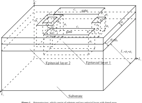
In the present time intensive decreasing of dimensions of elements of integrated circuits (p-n-junctions, field-effect and bipolar transistors et al) and their discrete analogs is occur [1-9]. To decrease dimensions of elements of integrated circuits are could use laser and/or microwave types of annealing (this types of annealing are intensively elaborating [10-12]), unsoundness of doped structure (for example, due to radiation damage [13] and appropriate references in this paper) et al. In the present paper we consider a heterostructure, which consist of a substrate and two epitaxial layers (see Figs. 1 and 2). The epitaxial layers including into itself four areas, which have been manufacturing by using another materials with dimensions ai (i=1 or 2) (in direction, which is perpendicular to interface between layers of heterostructure), bj (j=1, 2 or 3) and ck (k= 1 or 2). Two of these areas can be used as gate. Another two
areas could be used as source and drain after appropriate doping. One or two dopants have been infused into the two areas to produce required types of conductivities (p or n).It has been recently shown, that interface between layers of heterostructure under specific conditions and optimization of annealing time give us possibility to produce more homogenous distribution of dopant in doped area and decreasing of dopant concentration with higher speed after the doped area (one of consequence of the modification of dopant distribution is increasing of sharpness of p-n-junction, another consequence is increasing of homogeneity of dopant distribution in enriched area) [14-16]. Increasing of sharpness of p-n-junctions gives us possibility to decrease their switching times. Increasing of homogeneity of dopant distribution in doped area of p-n-junctions gives us possibility to decrease value of local overheats during functioning of their devices. The considered approach for manufacturing a field-effect transistor gives us possibility to decrease dimensions of this type of transistors in comparison with approach considered in [16] and all the more with approach considered in [1]. Main aims of the present paper are description of introduced construction of field-effect transistor and optimization of annealing time.
2. Method of Solution
Figure 1. Heterostructure, which consist of substrate and two epitaxial layers with doped areas
Figure 2. Appearance from side of heterostructure from Fig. 1
a
1
a
2
-a
1
L
x
-a
2
-a
1
c
1c
1c
2oxide
source
drain
gate
[image:2.595.80.542.82.418.2] [image:2.595.73.536.420.737.2](
, , ,
)
(
, , ,
)
(
, , ,
)
(
, , ,
)
j j j
j j j j
C C C
C x y z t
C x y z t
C x y z t
C x y z t
D
D
D
t
x
x
y
y
z
z
∂
∂
∂
∂
∂
∂
∂
∂
∂
∂
∂
∂
∂
∂
=
+
+
(1)with boundary and initial conditions
(
)
0
,
,
,
0
=
∂
∂
=
x j
x
t
z
y
x
C
,
(
)
0
,
,
,
=
∂
∂
=Lx x j
x
t
z
y
x
C
,
(
)
0
,
,
,
0
=
∂
∂
=
y j
y
t
z
y
x
C
,
(
)
0
,
,
,
=
∂
∂
=Ly y j
y
t
z
y
x
C
,
(
)
0
,
,
,
0
=
∂
∂
=
z j
z
t
z
y
x
C
,
(
)
0
,
,
,
=
∂
∂
=Lz y j
z
t
z
y
x
C
,
(2)(
x
y
z
)
f
(
x
y
z
)
C
j,
,
,
0
=
Cj,
,
.
HereCj(x,y,z,t) is the spatiotemporal distribution of concentration of dopant with number j (the first or the second);
D
Cj is the diffusion coefficient of dopant with number j. Value of dopant diffusion coefficient depends on properties of materials of layers of heterostructure, speed of heating and cooling of heterostructure (with account Arrhenius low). Redistribution of dopant is also depends on level of doping. Dependences of dopant diffusion coefficients on parameters could be approximated by the following function [8](
)
∏
(
(
)
)
+
=
=
j
i i
i i L
C
D
x
y
z
T
P
C
x
x
y
y
z
z
T
t
D
j j1
,
,
,
,
,
,
1
,
,
,
ξ
γγ (3)Here
D
Lj(
x
,
y
,
z
,
T
)
is the spatial (due to inhomogeneity of heterostructure) and temperature (due to Arrhenius low) dependences of diffusion coefficient of dopant with number j;P
jγ(
x
,
y
,
z
,
T
)
is the limit of solubility of dopant with number j; parameter γ depends on properties of materials and could be integer in the interval γ∈[1,3][8]. The parameter γcoincides with average electrical charge of defects, which interacting with atoms of dopant [8].
Let us determine spatiotemporal distributions of dopants by using method of averaging of function corrections (see, for example, [17] and appropriate references in this paper) with decreased quantity of iteration steps [18]. Framework the approach we consider distribution of dopant concentration with averaged dopant diffusion coefficient
D
0Lj( )
x
,
T
as the first-order approximation of solution of Eq.(1). The first-order approximation could be written as(
)
=
∑
∞( ) ( ) ( ) ( )
=1
1
,
,
,
2
n nC n n n nC
z y x
j
x
y
z
t
L
L
L
F
c
x
c
y
c
z
e
t
C
π
j j,
where
=
∫
x( ) ( ) ( ) (
∫
∫
)
y z
j j
L L L
C n
n n
nC
c
u
c
v
c
w
f
u
v
w
d
w
d
v
d
u
F
0 0 0
,
,
; cn(s) = cos (π n s/Ls);
( )
+
+
−
=
exp
2 2 01
21
21
2z y x L
nC
t
n
D
t
L
L
L
e
jπ
jjn
nCj 1
second-order approximation of dopant concentration
(
)
(
)
[
(
)
]
(
)
(
)
+
∏
+
+
=
=x
t
z
y
x
C
T
z
y
x
P
t
z
y
x
C
T
z
y
x
D
x
t
t
z
y
x
C
j ji i i C j L j i j
∂
∂
α
ξ
∂
∂
∂
∂
γ γ,
,
,
,
,
,
,
,
,
1
,
,
,
,
,
,
1 1 1 2 2(
)
[
(
(
)
)
]
(
)
+
∏
+
+
+
=y
t
z
y
x
C
T
z
y
x
P
t
z
y
x
C
T
z
y
x
D
y
j j i i i C jLj i
∂
∂
α
ξ
∂
∂
γ γ,
,
,
,
,
,
,
,
,
1
,
,
,
1 1 1 2 (4)(
)
[
(
(
)
)
]
(
)
∏
+
+
+
=z
t
z
y
x
C
T
z
y
x
P
t
z
y
x
C
T
z
y
x
D
z
j j i i i C jLj i
∂
∂
α
ξ
∂
∂
γ γ,
,
,
,
,
,
,
,
,
1
,
,
,
1 1 1 2Integration of left and right sides of Eq. (6) gives us possibility to obtain the second-order approximation of dopants concentrations in the following forn
(
)
(
)
[
(
(
)
)
]
(
)
+
∫
∏
+
+
=
=t j j
i i
i C j L
j
x
d
z
y
x
C
T
z
y
x
P
z
y
x
C
T
z
y
x
D
x
t
z
y
x
C
i j 0 1 1 1 2 2,
,
,
,
,
,
,
,
,
1
,
,
,
,
,
,
τ
∂
τ
∂
τ
α
ξ
∂
∂
γ γ(
)
2(
1(
)
)
1(
)
1 0
, , ,
, , ,
, , ,
1
, , ,
i j
t j
C i j
L j
i i
C x y z
C x y z
D x y z T
d
y
P x y z T
y
γ
γ
α
τ
∂
τ
∂
ξ
τ
∂
=∂
+
+
+
+
∏
∫
(4a)(
)
[
(
(
)
)
]
(
)
d
f
(
x
y
z
)
z
z
y
x
C
T
z
y
x
P
z
y
x
C
T
z
y
x
D
z
j i j Ct j j
i i
i C j
L
,
,
,
,
,
,
,
,
,
,
,
1
,
,
,
0 1 1 1 2+
∫
∏
+
+
+
=
∂
τ
τ
∂
τ
α
ξ
∂
∂
γ γThe average value of the second-order approximation could be determine by standard relation [17,18]
(
)
(
)
[
]
∫ ∫ ∫ ∫
−
Θ
=
Θ0 0 0 0 2 1
2
1
,
,
,
,
,
,
x y z
j
L L L
j j
z y x
C
L
L
L
C
x
y
z
t
C
x
y
z
t
d
z
d
y
d
x
d
t
α
.
(5)Substitution of the Eq. (4a) into Eq. (5) gives us possibility to obtain relation for the required average value
j С 2
α
(
)
∫ ∫ ∫
=
x y z jj
L L L C z
y x
С
L
L
L
f
x
y
z
d
z
d
y
d
x
0 0 0
2
1
,
,
α
.
(6)3. Discussion
Based on obtain in previous section relations we analyzed dynamics of redistribution of dopants in a semiconductor heterostructure. Typical distributions of dopants at fixed value of annealing time and different values of difference between dopant diffusion coefficients in different layers of heterostructure are presented in Fig. 3. The figure shows, that interface between layers of heterostructure gives us possibility to manufacture field-effect transistors with smaller in direction source-drain and into another directions. The introduced ejection of gate from line source-drain gives us possibility to decrease dimensions of transistor on this direction and depthward of heterostructure. However, dimensions of transistor in direction, which is perpendicular to line source-drain in flat of epitaxial layers, increases. In this situation one can obtain field-effect transistors with smaller thickness.
[image:5.595.315.554.192.436.2]Figure3.
Distributionsofdopantsinaheterostructurewithtwolayers for different values of difference between values of diffusion coefficients. Increasing of number of curve corresponds to increasing of difference between values of diffusion coefficients
Figure 4. Spatial distributions of dopant in heterostructure for diffusion doping. Curve 1 is idealized distribution of dopant. Curves 2-4 are real distributions of dopant for different values of annealing time (increasing of number of curves corresponds to increasing of value of annealing time)
Let us optimize annealing time to maximize effectiveness
of annealing of dopant. If annealing time is large, distribution of dopant became over homogenous. At the same time sharpness of p-n-junction decreases. If annealing time is small, distribution of dopant became over inhomogenous. Let us determine optimal annealing time framework recently introduce criterion [14-16,18]. Frameworks the criterion we determine real distribution of dopant by idealized stepwise one (curve 1 of Fig. 4) and minimize the following mean-squared error
(
) (
)
[
]
∫ ∫ ∫
Θ
−
=
L L Lx y zz y x
x
d
y
d
z
d
z
y
x
z
y
x
C
L
L
L
U
0 0 0
,
,
,
,
,
1
ψ
(7)
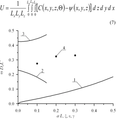
Figure 5. Dependences of dimensionless optimal annealing time, which have been calculated by minimization the mean squared error Eq. (6) on several parameters. Curve 1 is the dependence of optimal annealing time on the ratio a1/Lx (dependence of optimalannealingtimeontheratioa2/Lxis
thesimilartothedependenceona1/Lx)forpairwise equality of dopant
diffusion coefficients and ξ=γ=0, D1/DS=1. Curve 2 is the dependence of
optimal annealing time on the relation D1/DS (dependence of optimal
annealing time on the ratio D2/DS is the similar to the dependence on D1/DS,
where Di are the dopant diffusion coefficients in the epitaxial layers, DS is
the dopant diffusion coefficient in the substrate) for a1/Lx=1/2, ξ=γ=0.
Curve 3 is the dependence of optimal annealing time on the parameter ξ for pairwise equality of dopant diffusion coefficients and a1/Lx=1/2, γ=0, D1/DS
=1. Curve 4 is the dependence of optimal annealing time on the parameter γ
for pairwise equality of dopant diffusion coefficients and a1/Lx=1/2, ξ=0,
D1/DS=1
Where ψ(x,y,z) is the approximation function (curve 1 of Fig. 4). Dependences of optimal annealing time on several parameters are presented on Fig. 5. Optimal annealing time increases with increasing of thickness of epitaxial layers, because one can find increasing time of dopant diffusion through the epitaxial layers. Optimal annealing time decreases with increasing of the relation Di/DS with fixed their average value. In this situation increasing of value of dopant diffusion coefficient leads to acceleration of dopant diffusion in epitaxial layer. Increasing of parameter ξ leads to increasing of influence of concentrational dependence of dopant diffusion coefficient on diffusion process. In this situation one can obtain increasing of dopant diffusion
C
(
x
,Θ
)
0
a
1=
L
x/2
L
x1
2
3
L
x/4
3
L
x/4
C
(
x
,Θ
)
0
L
x2
1
3
[image:5.595.62.295.292.469.2] [image:5.595.62.293.523.690.2]of value of parameter γ leads to decreasing of influence of concentrational dependence of dopant diffusion coefficient on diffusion process, because dopant concentration is smaller, then limit of solubility of dopant. In this situation raising of the relation C(x,y,z,t)/P(x,y,z,t) into the power γ
decreases.
4. Conclusion
In this paper we introduce an approach to fabricate a field-effect transistor, which gives us possibility to decrease dimensions of the transistor in two directions and increase dimension of the transistor in the third one. However the increasing of dimensions did not compensate decreasing of full volume of the transistor. The approach based on changing of configuration of transistor, manufacturing of transistor in inhomogenous structure (for example, in heterostructure) and optimization of annealing time of infused dopants for production of the transistor.
Acknowledgments
This work is supported by the contract 11.G34.31.0066 of the Russian Federation Government and educational fellowship for scientific research.
REFERENCES
[1] A. Kerentsev, V. Lanin, Power Electronics. Issue 1. P. 34 (2008).
[2] A.O. Ageev, A.E. Belyaev, N.S. Boltovets, V.N. Ivanov, R.V. Konakova, Ya.Ya. Kudrik, P.M. Litvin, V.V. Milenin, A.V. Sachenko. Semiconductors. Vol. 43 (7). P. 897-903 (2009).
[3] Jung-Hui Tsai, Shao-Yen Chiu, Wen-Shiung Lour, Der-Feng Guo. Semiconductors. Vol. 43 (7). С. 971-974 (2009). [4] E..I. Gol’dman, N.F. Kukharskaya, V.G. Naryshkina, G.V.
Chuchueva. Semiconductors. Vol. 45 (7). С. 974-979 (2011). [5] T.Y. Peng, S.Y. Chen, L.C. Hsieh C.K. Lo, Y.W. Huang, W.C. Chien, Y.D. Yao. J. Appl. Phys. Vol. 99 (8). P. 08H710-08H712 (2006).
[6] W. Ou-Yang, M. Weis, D. Taguchi, X. Chen, T. Manaka, M. Iwamoto. J. Appl. Phys. Vol. 107 (12). P. 124506-124510 (2010).
[7] J. Wang, L. Wang, L. Wang, Z. Hao, Yi Luo, A. Dempewolf, M. M ller, F. Bertram, J rgen Christen. J. Appl. Phys. Vol. 112 (2). P. 023107-023112 (2012).
[8] Z.Yu. Gotra, Technology of microelectronic devices (Radio and communication, Moscow, 1991).
[9] A.B. Grebene, Bipolar and MOS analogous integrated circuit design. John Wyley and Sons, New York, 1983).
Chong, Appl. Phys. Lett. 89 (17), 172111-172114 (2006). [11] H.T. Wang, L.S. Tan, E. F. Chor. J. Appl. Phys. 98 (9),
094901-094905 (2006).
[12] Yu.V. Bykov, A.G. Yeremeev, N.A. Zharova, I.V. Plotnikov, K.I. Rybakov, M.N. Drozdov, Yu.N. Drozdov, V.D. Skupov. Radiophysics and Quantum Electronics. Vol. 43 (3). P. 836-843 (2003).
[13] E.L. Pankratov, E.A. Bulaeva. Int. J. Nanoscience. Vol. 11 (5). P. 1250028-1--1250028-8 (2012).
[14] E.L. Pankratov. Phys. Rev. B. Vol. 72 (7). P. 075201-075208 (2005).
[15] E.L. Pankratov. J. Appl. Phys. Vol. 103 (6). P. 064320-064330 (2008).
[16] E.L. Pankratov, E.A. Bulaeva. J. Comp. Theor. Nanoscience. Vol. 10 (4). P.888-893 (2013).
[17] E.L. Pankratov, E.A. Bulaeva. Appl. Nanoscience. DOI 10.1007/s13204-013-0228-7.