© 2017, IRJET | Impact Factor value: 5.181 | ISO 9001:2008 Certified Journal | Page 1418
Double Precision Floating Point Multiplier Using Verilog
Rishabh Jain
1, D. S. Gangwar
21
M.Tech Scholar, Dept. of VLSI DESIGN, F.O.T. Uttarakhand Technical University, Dehradun,India.
2
Astt. Prof., Dept. of VLSI DESIGN, F.O.T. Uttarakhand Technical University, Dehradun,India.
---***---Abstract -
Every computer has a floating point processor ora keen accelerator that satisfies the necessity of precision utilizing full floating point arithmetic. Decimal numbers are likewise called Floating Points in light of the fact that a single number can be represented with at least one significant digit relying upon the position of decimal point. In this paper we describe an implementation of double precision floating point multiplier IEEE 754 targeted for Xilinx Virtex-5 FPGA. The Platform used here is Verilog. The multiply process used here is pipelining, that gives the latency of eleven clock cycles.
1. INTRODUCTION
Floating-point representation includes encoding containing three fundamental parts: mantissa, exponent and sign. This involves a use of binary numeration and powers of 2 that outcomes infiguring floating point numbers representation as single precision (32-bit) and double precision (64-bit) floating point numbers. Both these numbers are characterized by the IEEE 754 standard. As indicated by the IEEE 754 standard, a single exactness number has one sign bit, 8 exponent bits and 23 mantissa bits where as a double precision number involves one sign bit, 11 exponent bits and 52 mantissa bits. In the majority of the applications we utilize 64-bit floating point to abstain from losing precision in a long succession of operations utilized as a part of the computation.
2
.
IEEE 754 FLOATING POINT STANDARD
The IEEE 754 floating-point standard is the most broadly utilized standard for floating-point calculations. The standard characterized an arrangement for floating-point numbers, unique numbers, For example, the infinite’s and NAN’s, an arrangement of floating-point operations, the rounding modes and five special cases. IEEE 754 indicates four organizations of portrayal: single precision (32-bit), double-precision (64-bit), single augmented (≥ 43 bits) and double expanded precisions (≥ 79 bits). Under this standard, the floating point numbers have three segments: a sign, an exponent and a mantissa. The mantissa has an understood shrouded leading hidden bit and the rest are division bits. The most utilized arrangements depicted by this standard are the single accuracy and the double-precision floating-point number configurations. In every cell the main number shows the quantity of bits used to represent each part, and the numbers in square brackets indicate bit positions saved for every segment in the single-precision and double– precision numbers.
Table -1: IEEE Floating Point Format
Format
Sign Exponent Mantissa Bias
Single-precision
1[31] 8[30-23] 23[22-0] 127
Double-precision
1[64]
11[62-
52]
52[51-0] 1023
3. DOUBLE PRECISION FLOATING POINT
MULTIPLIER
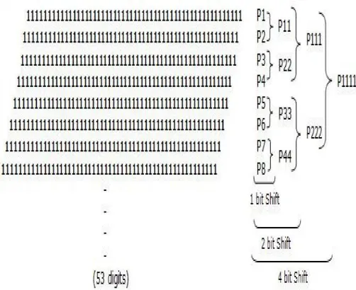
[image:1.595.309.560.530.735.2]The Floating Point Multiplier is implemented here without using DSP slices. The inputs a and b are broken up as sign (64th bit), exponent (63 – 52nd bits) and mantissa (51 – 0 bits). “Xor”ing the sign of a & b gives the final sign. Both inputs are checked if any or both of them are ‘0’, infinity, or Nan. This is done using two if–else statements. These checking’s are necessary to handle exceptions. The implicit ‘1’ is concatenated with the mantissa of a & b and the 53 partial products are calculated. Each partial product is calculated by ‘and’ ing mantissa of a with each mantissa bit of b replicated 53 times. The sum of the exponents, final sign, partial products and input exceptions are then registered in the first pipeline stage. The partial products now need to be added. Adjacent partial products are to be added with one bit shift.The resultant adjacent partial products after the 2 bit shift addition are to be added with 4 bit shift and so on.
© 2017, IRJET | Impact Factor value: 5.181 | ISO 9001:2008 Certified Journal | Page 1419
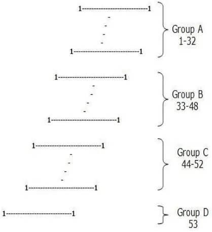
To add in this manner the number of partial [image:2.595.311.558.190.362.2]products should be a power of 2. Since 53 is not a power of 2, the partial products are divided as 32 + 16 + 4 + 1. Each group is added in the above mentioned method and the resultant 4 partial products are added with the required offset. Among the 4 groups the fourth group will be the same as the 53rd partial product as that group has only the final partial product.
Figure 2: Dividing 53 Partial Products into 4 groups.
While adding 2 adjacent partial products, for example: p3 and p4 in Fig.2 the LSB of p3 remains the same. Therefore while adding p3 and p4, the LSB of p3 (p3[0]) is concatenated at the right of the sum of p3(52:1) and p4.
Group A has 32 terms, therefore will have 16 additions. Group B has 16 terms, therefore will have 8 additions. Group C has 4 terms, therefore will have 2 additions. Group D will have no addition. All additions take place in parallel. The results are again registered. This is the second pipelined stage. In each stage adjacent terms are added with an increased amount of shift, with the shift equal to 2 (stage number – ‘1’). Suppose it is the fourth stage then the adjacent lower partial product is to be left shifted by 8 before adding. From Fig.11, p1111 = p111 + p222.
This can be broken down as p111[60:8] + p222 and concatenated with p111[7:0] at the right. In this way number of bit additions can be significantly reduced. After each stage of addition the values are registered to reduce the combinational path delay.
Though values of group D (53rd partial product), final sign, sum of exponents, input exceptions are calculated before the first pipeline stage, they also need to be
propagated through the pipeline as the values are required at a further stage.
Since group A has the maximum number of terms, it requires the most number of addition stages (5). Therefore we will have four intermediate partial products only after “1 + 5” (6) pipeline stages.
Figure 3: Final four intermediate partial products with their offsets
The four remaining intermediate partial products with their offsets are shown in Fig.4 Grouping them and adding as in previous cases will result in critical paths. Therefore the data is partitioned horizontally as shown in Fig.5
Figure 4: Final four intermediate partial products with horizontal partitioning
[image:2.595.53.262.197.426.2]© 2017, IRJET | Impact Factor value: 5.181 | ISO 9001:2008 Certified Journal | Page 1420
Group C and group D are then added. The least [image:3.595.324.539.97.271.2]significant 4 bits of group C require no addition. Bits(4 – 40) of group C and bits (0 – 36) of group D are added. The carry is taken and added with the remaining 16 bits of group C and group D. The result of group C and group D additions are concatenated and assigned to z. w,x,y,z, and the data coming through the pipeline are registered in the 7th pipeline stage.
Figure 5: Group AB and Group CD with Offset
Figure 6: Horizontal Partitioning of Y and Z
Leaving w and x as it is, y and z are again broken into two parts as shown in Fig.6 and added. The results are again registered in the 8th pipeline stage. Then the multiplication result is got by concatenating the intermediate results of w, x and (y + z). The MSB is then checked. If it is zero it needs to be shifted left by one. Only one shift is required because only normalized inputs are considered. The 105thbit will always be one if the 106th bit is zero. The results are again registered in the 9th pipeline stage.
Exceptions are considered in the next stage. If exponent bits are all ones and mantissa bits are all zeros, then the output is infinity. If exponent bits are all ones and mantissa bits are not all zeros, then the output is not a number (nan). Invalid is high if the inputs are invalid(this was calculated initially).
4. Simulation and Synthesis
[image:3.595.39.282.195.274.2]Essential to HDL design is the capacity to simulate HDL programs. Simulation permits an HDL description of a design (called a model) to pass design verification, a vital point of reference that approves the design's intended function (specification) against the code implementation in the HDL description. It additionally allows architectural exploration.
Figure 7: Block Diagram of Floating Point Multiplier
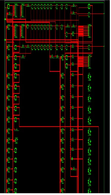
The detailed Register Transistor Logic (RTL) of the double precision floating point multiplier has been shown in figure 8.
In this RTL the number of slice registers used is only 10% of the whole FPGA virtex 5 kit, that is; only 3129 slices register are used out of 28800. Here the number of input output flip flops used is 69. The number of used slices here is only 19% , that is; 1388. The number of used logics is 10%, that is; 3150.
[image:3.595.37.266.316.417.2] [image:3.595.350.538.419.749.2]© 2017, IRJET | Impact Factor value: 5.181 | ISO 9001:2008 Certified Journal | Page 1421
[image:4.595.31.295.156.375.2]4.1 IMPLEMENTED RESULT
Table 2 Implementation result of Virtex5 (without
using DSP slices)
Logic
utilization Used Available Utilization Number of
Slices 3129 28,800 10%
Number of
Slice LUTs 4779 28,800 16%
Number of
used as Logic 3150 28,800 10% Number of
Occupied Slices 1388 7,200 19% Number of
fully used LUT-FF pairs
3101 4,807 64%
Number of
Bounded IOBs 198 480 41%
IOB Flip Flops 69 Number of
BUFG 1 32 3%
4.2 Timing Summary
In this timing summary analysis the multiplier used is without DSP Slices. The maximum synthesis frequency here we get is 141.33MHz. The maximum clock frequency that this Project using is 115.65 MHz. The design frequency here is 108.69 MHz. The minimum period of delay is 3.488nanoseconds.The minimum input arrival time before clock: 3.549nanoseconds. The minimum output required time after clock: 2.775nanoseconds.
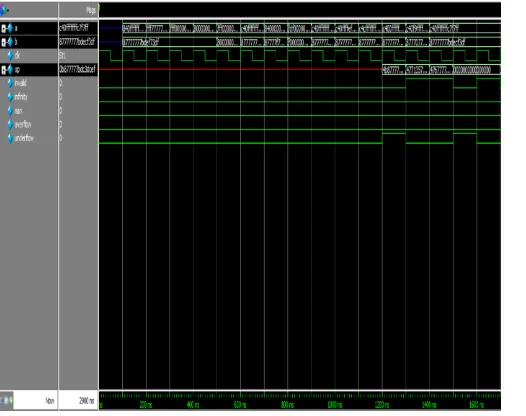
Figure 9: Simulation wave form(I) in Questasim 10.0b
5. CONCLUSIONS
In this project, the double precision floating point multiplier in light of the IEEE-754 format is successfully is effectively executed on FPGA. The modules are composed in Verilog HDL to enhance usage on FPGA. In this implementation they gained maximum frequency that of the multiplier executed by means of pipelining algorithm. Since the primary thought behind this implementation is to increase the speed of the multiplier by reducing delay at every stage using the optimal pipeline design, it gives the advantage of less delay in comparison to other method. The outcomes acquired utilizing the proposed calculation and usage is better as far as speed as well as far as hardware utilized. The maximum synthesis frequency here we get is 141.33MHz. The maximum clock frequency that this Project using is 115.65 MHz. The design frequency here is 108.69 MHz. The minimum period of delay is 3.488nanoseconds and the latency is of 11 clock cycle.
REFERENCES
[1]
IEEE 754 Standard for floating-point arithmetic, ANSI/IEEE Std 7541985 Vol ,Issue , 12 Aug 1985.[2]
B. Fagin and C. Renard, “Field Programmable Gate Arrays and Floating Point Arithmetic,” IEEE Transactions on VLSI, vol.2, no. 3, 365-367,1994.[3]
N. Shirazi , A. Walters, and P. Athanas, “ Quantitative Analysis of Floating Point Arithemetic on FPGA Based Custom Computing Machines,” Proceedings of the IEEE Symposium on FPGAs for custom computing machines(FCCM”96),pp.107-116,1996.[4]
A. Jaenicke and W. Luk,”Parameterized Floating-Point Arithmetic on FPGAs”, Proc. Of IEEE ICASSP,2001, vol. 2, pp. 897-900.[5]
M. Al- Ashrafy, A. Salem and W. Anis,“An Efficient Implementation of Floating Point Multiplier ” Electronics Communications and Photonics Conference(SIECPC) 2011 Saudi International, pp.15,2011.[6]
F.de Dinechin and B. Pasca. “Large multipliers with fewer DSP blocks in Field Programmable Logic and Applications”. IEEE, Aug. 2009.[7]
A. P. Ramesh, A. V. N. Tilak, A. M. Prasad ”An FPGA Based High Speed IEEE-754 Double Precision Floating Point Multiplier Using Verilog ” published in IEEE 978-1-4673-5301-4/13/© 2013IEEE. [image:4.595.38.301.512.720.2]© 2017, IRJET | Impact Factor value: 5.181 | ISO 9001:2008 Certified Journal | Page 1422
[9]
J. G. Prokais and D. G. Manolakis (1996),”DigitalSignal Processing: Principles, Algorithms and Applications”, Third Edition.