© 2017, IRJET | Impact Factor value: 5.181 | ISO 9001:2008 Certified Journal | Page 1903
DESIGN AND IMPLEMENTATION OF AN EFFICIENT CARRY SKIP ADDER
Jisney Sussan Joy
1, Premanand B
2,
1
Mtech scholar, Department of ECE, GECI, Kerala, India
2Assistant Professor, Department of ECE, GECI, Kerala, India
---***---Abstract –
Adders are fundamental unit in many computersystems. One of the most efficient adder architectures in terms of delay and area is the carry-skip adder. The existing CSKA structure uses concatenation and incrementation schemes to improve the speed and AOI (AND OR Invert) and OAI (OR AND Invert) compound gates are used instead of mux. In this project, an efficient 32-bit carry-skip adder to achieve high speed and low area consumption is designed. The higher speed is achieved by applying new adder in the middle stage and uses a simple and efficient gate-level modification to lower the area of the CSKA. The proposed structure makes use of Knowles adder and optimized RCA instead of utilizing Brent- Kung adder and normal RCA. The structure is realized with variable stage size technique, which improves the speed and energy parameter of the adder. Finally, an FFT is constructed using proposed carry skip adder which increases speed and reduces area usage. The delay of proposed hybrid CSKA is reduced by 38% compared to conventional CSKA and reduced to 16% compared to hybrid CSKA. The design is coded in Verilog HDL and its area and delay are analyzed using Xilinx ISE 14.2 Vivado Design Suite. The hardware simulation is done in Xilinx Spartan 3E FPGA.
Key Words: Carry Skip Adder, Hybrid Structure, Knowles Adder, Common Boolean Logic (CBL), FFT
1. INTRODUCTION
An adder is the basic component in VLSI circuits. An addition is an essential operation for any digital system, DSP or control system. Hence increasing speed and decreasing their power/energy consumption of adder has a high influence on speed and power consumption of processors. Adders carry out operations like addition, subtraction, multiplication, and division. Regarding the proficient implementation of an arithmetic unit, the binary adder becomes a very crucial hardware unit. Low-power and high-speed adder cells are used in battery operation based devices [1]. Now the biggest challenge is to lessen the power consumption of adder while preserving the high performance in circuit design. The selection of adder architecture to use is of ultimate importance, since the performance of adders may finalize the whole system performance.
One may pick between various adder families for optimizing power and speed. The Carry Skip Adder (CSKA) is one of the top efficient adders as its area usage and power consumption is identical to that of a Ripple carry adder
(RCA). The maximal combinational path delay of CSKA is lesser compared to RCA. Moreover, speedlimitation of CSKA confines its use in high-speed applications.
The traditional CSKA structure comprises of stages of RCA blocks and 2:1 multiplexer and all the RCA blocks are linked to each other through 2:1 multiplexers. The power consumed by the carry skip adder using multiplexer skip logic is more and critical pathdelay is high. The ripple carry adder is built by cascading number of full adders (FA)blocks in the series. One complete full adder is necessary for the addition of two binarydigits at different stage of the ripple carry. The carry output of one stage is fed directlyto the carry-in on the next stage. A number of full adder outputs are added to the ripplecarry adder circuit or ripple carry adders of different sizes may be cascaded in order toaccommodate the binary vector strings of larger sizes of adders. For an n-bit paralleladder, it needs n computational elements (FA). The carry is propagated in a serialcomputation. Hence, the delay is more as the number of bits is increased in RCA.
Comparing those adders, the best adder is CSKA because it requires less space and lower power consumption. The space and power consumption of CSKA is same as RCA, but delay path is finer and lower when compared to RCA. Comparing to PPA and CSLA circuits, power delay product of CSKA is lesser. Since CSKA is having less number of transistors, it has a simple layout and having less wiring length in comparison to other adder like CSLA and PPA [2].
Comparatively lower speed of carry skip adder limits its use for high-speed applications. The delay can be reduced by modifying its structure. The speed enhancement is realized by concatenation and incrementation method, also replaces the multiplexer skip logic which is used to execute the skip operation in conventional carry skip adder with the low power gates such as AOI and OAI. Thus the modified structure is known as concatenation and incrementation adder (CI-CSKA). The basic idea behind using CSKA structures was based on almost balancing the delays of paths such that the delay of the critical path is minimized. In hybrid CSKA structure, middle stage is replaced with a PPA [3]. The use of the fast PPA helps in increasing the speed of the adder structure.
© 2017, IRJET | Impact Factor value: 5.181 | ISO 9001:2008 Certified Journal | Page 1904 proposed hybrid latency CSKA is same as the hybrid
structure with the only difference in the nucleus stage and RCA block. Knowles adder is used for the construction of nucleus stage. Optimized RCA block is used for adder implementation. In the optimized RCA, Common Boolean Logic (CBL) based full adders (FAs) are used which offers minimum number of gates. By using proposed hybrid CSKA, an efficient Fast Fourier Transform is constructed and delay and area are optimized.
2. CARRY SKIP ADDER
[image:2.595.312.561.171.305.2]The carry skip adder comes from the group of a by-pass adder and it uses a ripple carry adder for an adder implementation [4]. The formation of carry skip adder block is realized by improving a worst-case delay. This adder is a proficient one in terms of to its area usage and power consumption. The structure of basic 4 bit carry skip adder is shown in Fig 1.
Fig -1: Four bit Carry Skip Adder
The CSKA may be implemented either using FSS or VSS technique where the maximal speed may be achieved for the VSS structure [3]. The stage size is the same as the RCA block size. In FSS technique, the size of all the stages is same. In VSS technique, the size of all stage differs from one another. By assigning variable sizes to the stages, the speed of the adder structure can be improved. The speed improvement can be realized by lowering the delays of the first and third blocks. These delays are lessened by reducing sizes of first and last RCA blocks.
2.1 Conventional CSKA
The conventional CSKA structure consists of RCA blocks and 2:1 multiplexer. RCA blocks, which is placed at one or more structure level are tied each other via a multiplexer. The skip operation is executed by multiplexer and logic gates. The input of the multiplexer is the carry input of the stage and the carry output of its RCA block. The product of propagation signals of the stage is used as the selector signals of the multiplexer. The carry skip adder can be implemented either using FSS or VSS technique, where the maximal speed is
[image:2.595.39.285.336.481.2]achieved for the VSS CSKA structure as shown in Fig 2. In the conventional carry skip adder, the skip logic with multiplexer exposes a large portion of critical path delay. The 2:1 multiplexer comprises more transistors that lead to increasing in area usage and power consumption.
Fig -2: Conventional Carry Skip Adder
2.2 Concatenation–Incrementation CSKA
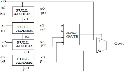
The structure is based on joining the concatenation and the incrementation schemes with the conventional-CSKA structure, and hence, is called by CI-CSKA [3]. The main aim of this method is to boost the speed and to enhance the efficiency of the conventional carry skip adder. The power consumption of the structure has to reduce without impacting the speed of it and also have to reduce the area and critical path delay. This structure grants us with the ability to use simpler carry skip logics. In conventional structure due to the usage of a multiplexer that acts as skip logic may force to a large critical path delay and area usage and large power consumption. These drawbacks are going to be resolved in the CI- CSKA by using compound gates instead of a multiplexer. The compound gates AOI and OAI acts as skip logic in order to reduce the area usage and delay of the skip logic in the conventional method. The structure has an appreciable lower propagation delay with a slightly smaller area compared with those of the conventional one. CI-CSKA can be implemented either using FSS or VSS technique. Fig. 3 shows the structure of VSS CI-CSKA.
© 2017, IRJET | Impact Factor value: 5.181 | ISO 9001:2008 Certified Journal | Page 1905 Fig -3: Variable CI-CSKA structure
2.3 Hybrid CSKA
The hybrid variable latency adder binds the PPA with the CI-CSKA hence the name hybrid [3]. The structure of hybrid latency CSKA is similar as the CI-CSKA structure with only one difference the nucleus stage is using PPA. The CI-CSKA structure may undergo further reduction of propagation delay and area by replacing middle stage of the structure with parallel prefix adder. In the hybrid structure shown in Fig. 4, the prefix network of the Brent–Kung adder is used for constructing the nucleus stage. One the advantages of this adder compared with other prefix adders is that in this structure, using forward paths, longest carry is calculated sooner compared with the intermediate carries, which are computed by backward paths. In addition, the fan-out of the adder is less than other parallel adders, while the length of its wiring is smaller.
Fig -4: Hybrid CSKA structure
3. PROPOSED HYBRID CSKA
The proposed hybrid CSKA structure exhibits higher speed by maintaining low power consumption and less area usage compared with that of hybrid CSKA. The speed enhancement was achieved by modifying the structure. The structure of proposed hybrid latency CSKA is same as the hybrid structure with the only difference in the nucleus stage and
[image:3.595.310.553.136.290.2]RCA block. The structure of proposed hybrid carry skip adder is shown in Fig. 5.
Fig -5: Proposed Hybrid Structure
A new type of parallel prefix adder network is used on the nucleus stage. Nucleus stage is the higher bit width stage on the variable latency network. Knowles adder shown in Fig. 6 is used for the construction of nucleus stage [5].
Fig -6: Structure of 8 bit Knowles Adder
[image:3.595.308.544.380.581.2] [image:3.595.41.283.488.640.2]© 2017, IRJET | Impact Factor value: 5.181 | ISO 9001:2008 Certified Journal | Page 1906 stage and thus cannot be removed. Black cells are the only
redundant cells in parallel prefix adders. In hybrid Knowles adder, the first stage is the Brent-Kung stage and rest are same as the Knowles adder stages. The features of two Adders are incorporated to get the best results. Also, Brent-Kung has more logic levels than that of Knowles adder. That’s why it was the worst design so far as compared to all other parallel Prefix adders.
The proposed hybrid CSKA uses optimized RCA block. In the optimized RCA, Common Boolean Logic (CBL) based full adders (FAs) are used which offers minimum no. of gates. The CBL FAs are designed by analyzing the truth table [7]. The CBL based FA is shown in Fig.7.
Fig -7: CBL based Full Adder
For the case of FAs when the carry input Ci=0 the sum output S=A XOR B, carry output Co=A&B and Ci=1, S= ~ (A XOR B), Co=A+B this concept is used to design the CBL FA. The CBL FA is also designed using 2:1 multiplexer with carry input Ci as a select input.
3.1 Application of proposed hybrid CSKA
A fast Fourier transform (FFT) algorithm computes the discrete Fourier transform of a sequence, or its inverse. FFTs are widely used for many applications in engineering, science, and mathematics. In FFT architectures, Butterfly unit is the essential block to calculate data addition and subtraction. An adder is the main building block of butterfly element. The basic requirement of adder is that it should be fast in operation and efficient in terms of chip area. So an efficient 8 point FFT is designed by using proposed hybrid CSKA to achieve less area consumption and high speed operation.
4. SIMULATION RESULTS
Simulation results of CSKAs and FFT are given below. Coding was done using Verilog HDL (Hardware Description Language). The hardware simulation is done in Xilinx Spartan 3E Field-Programmable Gate Array (FPGA) using the programming software ISE 14.2.
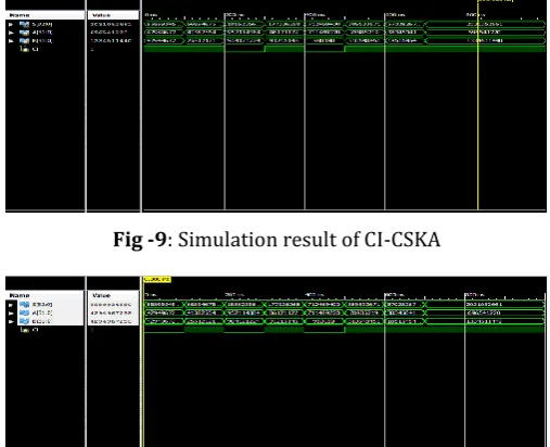
[image:4.595.307.561.157.274.2]Simulation results of Conv-CSKA, CI-CSKA, hybrid CSKA and proposed hybrid CSKA are shown in Fig. 8-11. A, B and Ci represent the input to the adder. S is the output for the given inputs. The simulation result obtained is same for all adders.
[image:4.595.38.282.283.400.2]Fig -8: Simulation result of Conv. CSKA
Fig -9: Simulation result of CI-CSKA
[image:4.595.306.560.312.518.2]Fig -10: Simulation result of hybrid CSKA
Fig -11: Simulation result of proposed hybrid CSKA
[image:4.595.307.556.574.668.2]© 2017, IRJET | Impact Factor value: 5.181 | ISO 9001:2008 Certified Journal | Page 1907 Fig -12: Simulation result of FFT
4.1 Performance Analysis
[image:5.595.307.564.119.384.2]Analysing the performance of the Conv-CSKA, CI-CSKA, hybrid CSKA and proposed hybrid CSKA in terms of area and delay are shown in the table: 1.
Table-1: Comparison Results of Different CSKA
Adders
Logic Utilization
No. of
slices No. of input LUTs
No. of bonded IOBs
Total Delay (ns)
Conv.CSKA 49 6 98 215 37
CI-CSKA
(fixed) 54 96 98 248 33
CI-CSKA
(variable) 56 93 98 247 30.1
Hybrid
CSKA 52 92 98 242 27
Proposed
CSKA 53 95 98 246 23.1
From the table it is obvious that the proposed hybrid CSKA has lower delay than the other CSKA architectures. The delay of proposed hybrid CSKA is reduced by 38% compared with conventional one and 14% compared with Hybrid CSKA. The area of conv. CSKA is less compared with other structures. The area of proposed hybrid CSKA is reduced by almost 1% compared with CI-CSKA but it is slightly increased by 1% compared with Hybrid CSKA. But when the middle stage adders compared, Knowles adder, the middle stage adder of proposed CSKA is more efficient than Brent Kung Adder, which is the middle stage adder of hybrid CSKA in terms of area and delay.
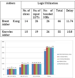
Table 2 shows comparison of middle stage adders. From the table it is clear that the area and delay of Knowles adder is less compared with Brent Kung adder. The area of Knowles is reduced by 16% compared with Brent Kung adder. The delay is reduced by 8% compared with Brent Kung adder.
Table -2: Comparison of middle stage adders
Adders Logic Utilization
No. of
slices No. of input LUTs
No: of bonded IOBs
Total Delay
Brent Kung
Adder 14 26 26 66 11.74
Knowles
Adder 10 19 26 55 10.8
Chart-1: Area comparison chart of Different CSKA
[image:5.595.37.288.330.539.2]Chart-2: Delay Analysis
Table 3 shows the comparison of delay and area of FFT with proposed CSKA and FFT with RCA adder.
Table -3: Comparison of FFTs No. of
slices No. of input LUTs
No. of bonded
IOBs
Total Delay
FFT
(RCA) 2294 4373 640 7307 61.47
FFT
[image:5.595.311.558.417.596.2]© 2017, IRJET | Impact Factor value: 5.181 | ISO 9001:2008 Certified Journal | Page 1908 From the table it is clear that the area and delay of FFT with
proposed CSKA is less compared with FFT with RCA adder. The area of FFT with CSKA is reduced by 2.7% compared with FFT with RCA adder. The delay of FFT with CSKA is reduced by 15.21% compared to FFT with RCA adder.
5. CONCLUSIONS
A new hybrid CSKA is designed that is more efficient in terms of speed and chip area. Proposed hybrid CSKA is implemented and compared with existing CSKA architectures. This structure uses Knowles adder for the construction of the middle stage and optimized RCA for adder implementation. The efficient Fast Fourier Transform is constructed using modified CSKA adder structure and area and delay are optimized. Proposed CSKA is implemented and simulated in Xilinx ISE 14.2 using Verilog HDL. The delay of proposed structure is reduced by 38% compared to conventional CSKA and is reduced by 14% compared to hybrid CSKA. The area of proposed CSKA is reduced by almost 1% compared to CI CSKA structure. When the proposed structure is used in FFT, the area is reduced by 2.5% and delay is reduced by 15%.
REFERENCES
1. B. Roja Rao, V. Prasad, “Implementation of Carry Skip Adder using High-Speed Skip Logic at Different Level”, International Journal of VLSI System Design and Communication Systems, issue 9, pp. 840-843, 2016. 2. M. Alioto and G. Palumbo, “A simple strategy for
optimized design of one-level carry-skip adders” IEEE Trans. Circuits Syst. I, Fundam Theory Appl.,vol. 50, no. 1, pp. 141–148, Jan.2003.
3. Milad Bahadori, Mehdi Kamal and Ali Afzali- Kusha, “High-speed and energy efficient carry skip adder operating under a wide range of supply voltage levels”, IEEE Transaction on Very Large Scale Integration (VLSI) Systems, vol. 24, no. 2, pp. 421-433, 2016.
4. Monisha T. S., Senthil Prakash K. “An Optimized Design of High-Speed and Energy- Efficient Carry Skip Adder with Variable Latency Extension”, International Journal of Science and Research, vol. 5, issue 3, pp. 329-33, 2016.
5. S. Knowles “A family of adders”, in Proceedings of the 15th IEEE Symposium on Computer Arithmetic, pp.277– 284, 2001.
6. Pawan Kumar and Jasbir Kaur, “Design of Modified Parallel Prefix Knowles Adder”, International Journal of Science & Research, vol. 3, pp. 199-201, 2014.
7. N. Vijayabala and T. S. Saravana Kumar “Area minimization of carry select adder using Boolean algebra” International Journal of Advances in Engineering & Technology, July 2013.
8. V. Kantabutra, “Designing optimum one-level carry-skip adders”, IEEE Trans. Comput., vol. 42, no. 6, pp. 759– 764, 1993.