Volume 55– No.7, October 2012
Probabilistic Defect Analysis Model for Quantum dot
Cellular Automata Design at Analytical Phase
Arijit Dey
B.P.Poddar Institute ofManagement and Technology, 137, VIP Road, Kol-700052, India
Kunal Das
B.P.Poddar Institute ofManagement and Technology, 137, VIP Road, Kol-700052, India
Debashis De
West Bengal University of Technology, BF-142, Sector-I, Salt Lake City, Kolkata 700064, IndiaMallika De
Department of Engg.andTechnological Studies, Kalyani University, Kalyani 741235, West
Bengal, India
ABSTRACT
The advantage of defect analysis on Quantum dot Cellular Automata(QCA) is that defects can be predict (which are probable to arise during fabrication phase) at analytical phase of QCA design. Since QCA is probabilistic in nature, the probability theory is introduced here to analyze the defect/fault tolerance at gate level of QCA design. We proposed a Bayesian network based Probabilistic Defect Analysis Model (PDAM) to analyze the defect at analytical phase of QCA design. Proposed model is applied over QCA wire, three input Majority voter, Five Input Majority voter and the result is compared with QCADesigner to justify the importance of PDAM approach over exhaustive simulation process with QCADesigner.
Keywords
Radius of effects; Five Input Majority Voter; Bayesian Network; PDA Model; Conditional probability
1. Introduction
Quantum dot Cellular Automata (QCA) is becoming emerging technology in the field of nano scale computing. In 1993, C. S. Lent et al proposed the QCA as an alternative nano computing paradigm [1-3]. An exhaustive research is conceived during a decade and becomes research interest. Several proposals have been reported to design the QCA Device fabrication [4-5], Logic implementation [6-13], and testing [14-23] etc. the fundamental theory of computation for QCA is a cell, consisting of two extra electrons confined within square shape four quantum dot systems. The device cell design is such that (figure 1.a) the electrons (4M + 2) are confined within cell and can’t able to tunnel outside cell unlike with CMOS technology, where ‘M’ is number of electrons in each QD and ‘2’ is extra electrons injected (extra number). Due to the position of QD in a square shape cell (four corner of square) the two extra electrons have only two choices as shown in figure 1.b, these two state are denoted ‘+1.00’ polarization and ‘-1.00’ polarization and corresponding Logic state are defined as State 1 and 0. Logic gate design involved affect of neighboring cells coulumbic interaction (for example Majority Voter ‘MV’ shown in figure 1.c). The ground state configuration can be described by Knik energy. The Knik energy is inversely proportional to distance between two charge qi, qj defined as
(1)
Where ε0, εr are permittivity of free space and relative permittivity respectively. For QCA Logic gate design need four adiabatic clocking namely Relax, Switch, Hold and Release phase. This clock conflict can be the cause of error at gate level as well as circuit level.
The 3 X 3 tile nano structure in QCA is found to be most promising design approach [16-18]. In early there are several proposal have reported. 3 X 3 tile structure is becoming empirical due to its robustness and versatile logic implacability. 3 X 3 tile structure can be classified in terms of active and passive categories. Active type 3 X 3 tile are those the computational part took place, namely orthogonal tile [17], triple input majority voter [17], five input majority voter [16,18], and coupled majority-minority voter [16]. On the other hand passive type are those no computation is took place rather processed by wire, passive type tile are namely double fan out tile [17], triple fan out tile [17], baseline tile [17], fan in tile [17], symmetrical-asymmetrical tile [17].
Defects are basically uncertainty, which is probable to occur in any VLSI design. QCA design is not also out of this list. The different issues in QCA defects are considers on chemical synthesis phase and deposition phase. The gate level and logic level, the defect test with exhaustive simulation is reported in early reports [16]. In this paper our attempt is to introduce probabilistic approach for defect analysis at analytical phase in QCA with an Artificial Intelligence tool Bayesian Network that permits probability and statistical method to deal with defects in QCA circuits. S. Bhanja et al. represents QCA circuit at layout level of Bayesian Network model[27-34].In this paper, the different probability of defect like extra cell deposition, Missing cell deposition, Misplacement of cell deposition at gate level has been studied. The Probabilistic Defect Analysis Model with Bayesian Network is reported. The comparison is made between exhaustive simulation result (with simulator QCA Designer [35]) and proposed Probabilistic Defect Analysis Model (PDAM).
j i j i r kink
j
i
q
q
r
r
E
|
|
4
1
0
Figure 1 (a) QCA cell design with tunnel junction, (b) QCA cell with two possible state polarization, (c) Three Input Majority Voter, (d) QCA wire and (e) Five Input Majority
Voter.
2. Probabilistic Defect Analysis Model at
Analytical Phase
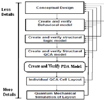
[image:2.595.56.295.72.236.2]QCA design methodology is considered to have following steps in ‘Analytical phase’ as shown in figure 2. The conceptual design of logic gate, Create and Verify Behavioral model, Create and verify structural logic model, Create and verify structural QCA model, Individual QCA cell Layout and Quantum Mechanical simulation of Layout are different steps in QCA design [28-34]. In our work we introduce a Probabilistic defect analysis model (PDAM) into the analytical phase since the basic operation of QCA is probabilistic in nature.
Figure 2 Different steps at Analytical phase of QCA design methodology
Let us assume that ‘N’ be the number QCA cells {X1,X 2, …, XN} arrange in definite structure such that it produce a certain logic operation like wire, Majority Voter etc. in QCA (shown in figure 1). Now we can represent the QCA layout in terms of Direct Acyclic Graph (DAG). All DAG can easily represent in terms of probability and statistical tool Bayesian Network [36].
number of nodes {X1,X 2, …, XN}, the directed edge between two nodes implies direct dependency of XN over XN-1. The direction represents cause-effect relationship. If we consider a node XN-1 (cell XN-1) the conditional probability table (CPT) is shown in table 1.
Table 1 CPT for Node XN
It reflect that if node XN-1 (cell in case of QCA layout) is Low = 1.0 and High = 0.0 then conditional probability XN to be Low = 1.0 and High = 0.0, and if XN-1 is High = 1.0 and Low = 0.0, the conditional probability is high = 1.0, low =.0. The joint state probability function can be decomposed into product of conditional probability function represented by
))
(
(
)
,....
,
(
1 2
1 a k
N k
N N
P
x
P
x
x
x
x
P
(2)
As a result if we consider a wire with ‘N’ number of nodes there might possible corresponding Bayesian Network model with (N-1) cell radius of influence. If we consider one cell radius of influence, then a conditional probability
)
(
)
|
(
...
)
|
(
)
|
(
)
,....
,
(
x
1x
2x
P
x
x
1P
x
1x
2P
x
2x
1P
x
1P
N
N N
N N
(3)
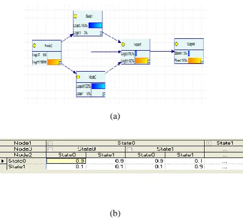
[image:2.595.346.549.149.188.2]In our work, we consider one cell radius of influence due to Knik energy and Radius of effect. The Fault/ Defect model is establish as following way. Let us consider the Bayesian Network with one cell radius of influence for a simple wire as shown in figure 3, X1, X2, X3 are three nodes known as intermediate node. We assume for full polarization value is ±0.9 to ±1.00, partial polarized value ±0.8 to ±0.5 and no polarization -0.5 to +0.5. We include Decision (1) and Utility (U) nodes for evaluating Logic 1/0 probability at output. The ‘Probabilistic Defect Analysis Model’ is setup with injecting extra faulty node known as ‘Mutant’ into the intermediate nodes. Consider the defect that might influence the other node to generate probability of defects at output. Let us consider the conditional probability table (CPT) for INJ as follows:
Figure 3 Defect model setup for QCA wire with probabilistic Bayesian network.
Table 2 CPT for Node INJ
XN-1 Low High
Low 1 0
High 0 1
X1 Low High
Low 0.9 0.1
[image:2.595.60.242.480.654.2] [image:2.595.313.567.563.776.2]Volume 55– No.7, October 2012
Table 2 implies that when X1 is Low (Logic 0) the conditional probability of INJ is 0.9 to hold Low (Logic 0) and it have the probability 0.1 to hold High (Logic 1) and similarly for rest of the cases. As a result the Decision and Utility nodes for evaluating Logic 1 & Logic 0, probability decreases at the output node with Mutant node.
If we change the entries in table 2 0.9 to 0.7 and 0.1 to 0.3 the corresponding result for Logic 0 and Logic 1 probability at output with that Mutant node/ Fault Injected node is 0.66/0.34 value. Hence we can conclude that the probability of defect injected (may occur in chemical synthesis phase or deposition phase) into the DAG base Bayesian Network up to certain percentage of defect the o/p probability for evaluating Logic 1 and Logic 0 is adequate. This is known as upper bound of probability that the network can persist and output probability for evaluating Logic 1 or Logic 0.
3. Study on Defect Analysis of QCA Logic
Gate at Analytical Phase
In this section, we study on defects at gate level in analytical phase of QCA design with the proposed model as well as a traditional QCADesigner base QCA simulation. The Analytical Phase may consider before fabrication of device or gate, a prediction of defects/ fault tolerance can be measured with mathematical model. The probabilistic model based on Bayesian Network for wire with one cell influence have been discussed in last section, here we analyze defects on the three input Majority Voter[17] and Five Input Majority voter[16]. The possible defect that are probable to occur during deposition phase like (a) Extra cell deposition, (b) Missing cell deposition, (c) Misplacement of cell deposition are discussed with probabilistic model.
3.1
Three
Input
Majority
voter
or
Traditional MV
[image:3.595.314.552.466.685.2]The Bayesian Network for probabilistic analysis is shown in figure 4.a, the network or DAG consists of input XA, XB, XC and output node for MV is Xout , the intermediate node/ cell is Xint. The conditional probability considering one cell influence is defined as
)
(
)
(
)
(
)
,
,
|
(
)
|
(
)
,
,
,
,
(
x
Ax
Bx
Cx
intx
outP
x
outx
intP
x
intx
Ax
Bx
CP
x
AP
x
BP
x
CP
(4)
The probability for Logic 0 & Logic 1 for (101) input combination is consider 0.0 & 1.0, 1.0 & 0.0 and 0.0 &1.0 respectively. This is considering the maximum of probability input and the corresponding definition of node Xint is shown in figure 4.b, consider for exact design i.e., no error/ effects are taken into account. The decision from the above model is similar with QCADesigner[35] result. Hence, it suggests that the probabilistic study with Bayesian network model provide mathematical model at analytical phase for QCA. For defect analysis, let us inject defect into the exact network model as shown in figure 4.a. The setup is to generate the fault/ defect model with Bayesian Network. The different defects that may be injected into the defined model are 1. Missing cell deposition: intermediate cell are missed, 2. Extra cell deposition: extra cell that may be injected, 3. Misplacement cell deposition: cells are misplaced. The above mention defects are actually occurs during fabrication phase of QCA design. We analyze these with QCADesigner and this proposed model.
(a)
(b)
Figure 4 (a) Bayesian Network representation of three input Majority Voter. (b) CPT for Xint
3.1.1 Missing cell deposition
For missing cell deposition, the defect model is setup such that one or few node are missing in Bayesian Network. The Bayesian Network model is shown in figure 5.a. The intermediate cell Xint1 is missing and the corresponding conditional probability table for the node Xint2( in figure 5.a Xint2 is denote as Node4) is defined as shown in figure 5.a. The influence of node XA is for Logic 1 & Logic 0 considered to be reduced from 1.0 to 0.8/0.9 and 0.0 to 0.1/0.2 respectively. The result shows in figure 6 and table 3. This is compared with simulation result of QCADesigner.
(a)
(b)
Figure 6 comparisons with simulation of QCADesigner and Decision Result from PDAM for Missing cell deposition defect
3.1.2 Extra cell deposition for Three Input
Majority voter
Extra cell deposition is fault that an extra cell that probable to deposited, Let Xext1, Xext2, Xext3, Xext4 be the four extra maximum to occur (shown in figure 7). The result is shown in table 4 and figure 8. The simulation result with QCADesigner is compared with the decision of Probabilistic Defect Analysis Model (PDAM).The result shows that Probabilistic Defect Analysis Model with Bayesian Network produce correct decision for defect analysis at Analytical phase of QCA design.
Figure 7 Three input Majority voter with extra cell deposition is shown with Bayesian network model.
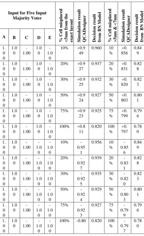
Input for Three Input Majority Voter
%
Mi
ss
in
g
c
ell
d
ep
o
siti
o
n
fr
o
m
th
e
ex
a
ct
la
y
o
u
t
S
im
u
la
ti
o
n
r
esul
t
fo
r
Q
CA
De
sig
n
er
O
u
tp
u
t
ce
ll
De
cisio
n
r
esul
t
fr
o
m
Ba
y
esia
n
n
etwo
rk
Mo
d
el
A B C
1.00 1.00 -1.00 10% +0.95 0.900
1.00 1.00 -1.00 30% +0.95 0.900
1.00 1.00 -1.00 50% +0.95 0.900
1.00 1.00 -1.00 75% +0.95 0.900
1.00 1.00 -1.00 100% No polariz. 0.500
-1.00 1.00 -1.00 10% -0.95 0.900
-1.00 1.00 -1.00 30% -0.95 0.900
-1.00 1.00 -1.00 50% -0.95 0.900
-1.00 1.00 -1.00 75% -0.948 0.000 -1.00 1.00 -1.00 100% No polariz. 0.500
Input for Three Input Majority Voter
%
ex
tr
a
c
ell
d
ep
o
sitio
n
fr
o
m
th
e
ex
a
ct
la
y
o
u
t
S
im
u
la
ti
o
n
r
esul
t
fo
r
Q
CA
De
sig
n
er
O
u
tp
u
t
ce
ll
De
cisio
n
r
esul
t
fr
o
m
Ba
y
esia
n
n
etwo
rk
Mo
d
el
A B C
1. 0 0
1.00 -1.00 10% +0.953 0.900
1. 0 0
1.00 -1.00 20% +0.953 0.900
1. 0 0
1.00 -1.00 30% +0.953 0.900
1. 0 0
1.00 -1.00 50% +0.953 0.900
1. 0 0
1.00 -1.00 75% +0.953 0.900
1. 0 0
1.00 -1.00 100% +0.953 1.000
1. 0 0
-1.00 -1.00 10% -0.953 0.900
1. 0 0
-1.00 -1.00 20% -0.953 0.900
1. 0 0
-1.00 -1.00 30% -0.953 0.900
1. 0 0
-1.00 -1.00 50% -0.953 0.900
1. 0 0
-1.00 -1.00 75% -0.953 0.900
1. 0 0
-1.00 -1.00 100% -0.953 1.000
[image:4.595.49.273.102.525.2]Input Majority Voter
[image:4.595.299.557.293.761.2]Volume 55– No.7, October 2012
Figure 8 Comparisons with simulation of QCADesigner and Decision Result from PDAM for extra cell deposition defect
3.1.3 Misplacement cell deposition
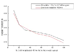
Misplacement cell deposition is defect that probable to occur during deposition phase of fabrication process. Let Xint1, Xint2 be two intermediate cell, XA ,XB ,XC are three input of three input MV and Xout is output cell. Misplacement of 10% cell to 100% cell is considered in our study. We also consider that the displacement are <5nm and >5nm & <7nm. The conditional probability table for displaced/misplaced cell is considered as discussed in last section. The result is shown in table 5. The simulation result with QCADesigner is also compared with the decision of Probabilistic Defect Analysis Model (PDAM) for misplacement is shown in figure 9. The result suggest that Probabilistic Defect Analysis Model with Bayesian Network produce correct decision for defect analysis at Analytical phase of QCA design and 10% cell misplacement with <5nm displacement are allowable defect tolerance.
[image:5.595.56.274.74.218.2]Figure 9 comparisons made with simulation of QCADesigner and Decision Result from PDAM for
[image:5.595.115.241.477.568.2]misplaced cell deposition defect
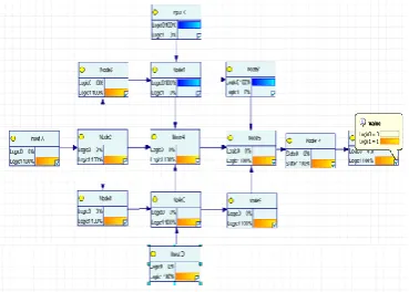
Figure 10 Bayesian network model for Five Input Majority voter.
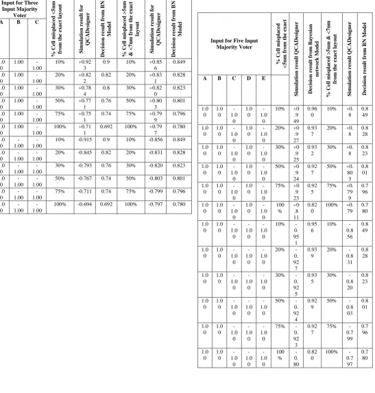
3.2 Five Input Majority Voter
In this subsection we discuss with fault/ defect probability that are probable to occur during fabrication. In our early work we introduce an innovative Five Input Majority voter [16]. Here we consider Five Input Majority Voter for probabilistic analysis of defect. In the analytical phase, we explore the PDAM for Five Input Majority Voter. Several errors that may arise in fabrication are (i) Misplacement cell deposition (ii) Missing cell deposition (iii) Extra cell deposition. The PDAM for Five Input Majority voter helps QCA fabricator to know the robustness and fault tolerance of that device before fabrication at analytical phase. It will provide a guideline about the allowable tolerance. Rest of this subsection provides the probabilistic analysis with Bayesian network as well as QCA cell Layout analysis with QCADesigner.
Let us consider the Bayesian Network for probabilistic analysis is shown in figure 10. The network or DAG consists of input XA, XB, XC, XD, XE and output node for MV is Xout, the intermediate node/ cells are Node1 ,... , Node9. The probability for Logic 0 & Logic 1 for (101) input combination is consider 0.0 & 1.0, 1.0 & 0.0 and 0.0 & 1.0 respectively. Consider for exact design i.e., no error/ effects are taken into account. The decision from the above model is similar with QCADesigner result. Hence, it is suggest that the probabilistic study with Bayesian network model provide an analytical phase mathematical model for QCA. For defect analysis, let us inject defect into the exact network model as shown in figure 10. The setup is to generate the fault/ defect model with Bayesian Network. The different defects that may be injected into the defined model are 1. Missing cell deposition- intermediate cell are missed. 2. Extra cell deposition- extra cell that may be injected. 3. Misplacement cell deposition- cells are misplaced. The above mention defects are occurs during fabrication phase of QCA design as mentioned in last section. We analyze these with QCADesigner and this proposed model.
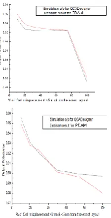
3.2.1 Misplacement cell deposition defect
[image:5.595.121.222.620.699.2]Figure 11 the possible output from Simulation result with QCADesigner and Decision result from Proposed PDAM for (a) cell misplacement <5nm and (b) cell misplacement >5nm & <=7nm.
3.2.2 Missing cell deposition defects
The Bayesian Network model is shown in figure 12.a. The intermediate cell (out of Node1 ,... , Node9) Node1 is missing. For missing cell defect analysis the influence of node XA is for Logic 1 & Logic 0 considered to be reduced from 1.0 to 0.9(<5nm cell displacement)/0.8(>5nm &<7nm cell displacement) and 0.0 to 0.1/0.2 respectively which is considered to 10% cell misplacement. The result shows in figure 12.b and table 7. These results are conformed to simulation result of QCADesigner.
(a) (b)
Figure 12 (a)Bayesian Network with missing cell defect (b) comparison with simulation of QCADesigner and Decision Result from PDAM for Missing cell deposition defect
3.2.3 Extra cell deposition defect on Five Input
majority Voter
Extra cell deposition is fault that an extra cell that probable to deposited, Let Xext1, Xext2, Xext3,… XextN be the N extra cell may arise. The setup is same as with three input majority voter. The result is shown in table 8. The simulation result with QCADesigner is compared with the decision of Probabilistic Defect Analysis Model (PDAM).The result shows in figure 13
produce correct decision for defect analysis at Analytical phase of QCA design.
Figure 13 comparisons with simulation of QCADesigner and Decision Result from PDAM for extra cell deposition defect
4. RESULT AND DISCUSSION
[image:6.595.108.221.71.293.2]In this section, we describe our results that are obtained in our work. The Probabilistic Defect Analysis Model based on Bayesian Network considered for defect analysis at analytical phase. In case of QCA wire, we have shown that extra faulty node/cell known as ‘Mutant’ is inserted into the intermediate node. ‘Mutant’ is a fault injected into the QCA wire. Defect or faulty node will influence the other node to drive defects at output. Here we introduce defect in terms of reduction of probability to produce logic ‘0’ or logic ‘1’ at the output into the CPT. In case of three input Majority voter for example, the different defects that are considered are (i) Missing cell Deposition: the figure 6 implies that the missing cell deposition with different ‘%’ of missing cell deposition has no such effect unless the 100% missing cell deposition, it produce the no polarization. Comparison is made with QCADesigner result at layout level and with PDAM result. It implies that our proposed model provide the correct decision. (ii) Extra cell deposition: The decision made with PDAM is shown in the figure 8, it implies that same as missing cell deposition defect stated early. (iii) Misplacement cell deposition: The figure 9 shows that the ‘%’ of cell misplacement deposition with displacement <5nm up to 10% -15%. The result provides the defect tolerance limit to QCA fabricator. On the other hand, five input Majority voter provide much more fault tolerance. The figure 11 (a) suggest that the PDAM result as well as QCADesigner result provide around 75% misplacement defect tolerance with displacement <5nm, missing cell deposition for the same have defect tolerance around ‘50% cell missing deposition’ and for extra cell deposition, there is no such effect is noticed. It implies that five input Majority voter design is provide much more reliable.
5. CONCLUSION
[image:6.595.313.532.106.204.2] [image:6.595.55.273.502.591.2]Volume 55– No.7, October 2012
input majority voter and five input majority voter. The tolerance is reported with PDAM for the above gates are adequate and verified, conformed with QCADesigner result. Hence, we conclude that our study with PDAM at analytical phase of QCA design may consider as decision making step for defect analysis at gate level. Our future work will concentrate on circuit level PDAM at analytical phase of QCA design.
REFERENCES
[1] C. S. Lent, P. D. Taugaw, W. Porod, and G. H. Bernstein (1993) Quantum dot cellular automata Nanotechnology.4: 49-57.
[2] C.S. Lent, P.D. Tougaw and W. Porod(1993) Appl Phys Lett.62:7-14.
[3] C. S. Lent, P. D. Taugaw (1996) Dynamic behavior of quantum cellular automata J. Appl. Phys. 80(8): 4722-4736.
[4] Amlani et.at. (1999) Experimental demonstration of electron switching in a quantum-dot cellular automata (QCA) cell Superlattices and Microstructures. 25(1-2): 273-278.
[5] M.Macucci et al. (2003) A QCA cell in Silicon on insulator technology: theory and experiment, Elsevier Superlattices and Microstructure. 34: 205-211.
[6] M. Momenzadeh, M. Ottavi, F. Lombardi (2005) Modeling QCA Defects at Molecular-level in Combinational Circuits, Proc. 20th IEEE International Symposium on DFT, pp.208-216.
[7] J. Huang, M. Momenzadeh, L. Schiano and F. Lombardi, Simulation-based design of modular QCA circuits, Proc. of IEEE conference on nanotechnology, Nagoya, 2005. [8] C. S. Lent, P. D. Taugaw, W. Porod, and G. H. Bernstein
(1993) Quantum cellular automata, Proc. Nanotechnology. 4: 49-57.
[9] Momenzadeh, M.; Jing Huang; Tahoori, M.B.; Lombardi (Dec. 2005) Characterization, test, and logic synthesis of and-or-inverter (AOI) gate design for QCA implementation, Computer-Aided Design of Integrated Circuits and Systems, IEEE Trans. 24:1881-1893. [10]C.S. Lent et al (2002) Power gain and dissipation in
quantum-dot- cellular automata, J. Appl. Phys. 91(2):823-831.
[11]K.Das and D.De (February & April 2011) A study on Diverse Nanostructure for Implementing Logic gate design for QCA, Int. Journal of Nanoscience, World Scientific. 10(1-2): 263-269.
[12]K.Das and D.De, A Novel approach of And-Or-Inverter (AOI) gate design for QCA, Proc. IEEE conf. CODEC-09. (14-16 Dec2009)ISBN 978-81-8465-152-2, pp.1-4. [13]K.Das, D.De (2010) Characterization, Test and Logic
Synthesis of Novel Conservative & Reversible Logic Gates For QCA, Int. Journal of Nanoscience, World Scientific. 9(2): 1-14.
[14]K.Das, D.De, Novel Approach to Design A Testable Conservative Logic Gate for QCA Implementation. Proc. IEEE Intr. Conf. of IACC’2010. (19th Feb.-20th Feb. 2010), pp.82-87.
[15]K.Das, D.De (2010) QCA Defect and Fault Analysis of Diverse Nanostructure for Implementing Logic Gate, Int. journal of Recent Trends in Engineering, Finland. 3(1):1-5.
[16]Kunal Das, Debashis De (2011) Characterization, applicability and defect analysis for tiles nanostructure of quantum dot cellular automata, Molecular Simulation, 37(3): 210 – 225.
[17]Huang et al. (6 June 2007) On the Tolerance to Manufacturing Defects in Molecular QCA Tiles for Processing-by-wire, Journal of Electronic Testing: Theory and Applications (JETTA). 23(2):163-174.
[18]Kunal Das, Debashis De, Mallika De " Tile Based Approach To Design Logic Circuit And It’s Defects Analysis For Quantum Dot Cellular Automata ", In Quantum Dots and Quantum Cellular Automata: Recent Trends and Applications, Nova Science Publishers, Inc., USA. [In press]
[19]M.B Thoori, J.Huang, M.Momenzadeh, and F.Lombardi (Dec.2004) Testing of quantum Cell automata,IEEE Trans. Nanotechnol. 3(4): 432-442.
[20]X. Ma, J. Huang, C. Metra, F.Lombardi (Jan 2008) Reversible Gates and Testability of One Dimensional Arrays of Molecular QCA, Springer Journal of Electronic Testing.24:1-3.
[21]Ma X. et al. (February 2009) Detecting multiple faults in one-dimensional arrays of reversible QCA gates, Journal of Electronic Testing: Theory and Applications (JETTA). 25(1):39-54.
[22]Ma X. et al. Testing reversible 1D arrays for molecular QCA, Proc. IEEE International Symposium on Defect and Fault Tolerance in VLSI Systems. art. no. 4030917(2006), pp. 71-79.
[23]N.Jha and S.Gupta Testing of Digital system, .Cambridge, united kingdom; Cambridge university press.(2003). [24]Tougaw, P. Douglas, Lent, Craig S (Feb 1994) Logical
devices implemented using quantum cellular automata, Journal of Applied Physics. 75(3):1818-1825.
[25]J.Timler and C.S.lent (2002) power gain and dissipation in quantum dot cellular automata, J. of App.phy. 91(2): 823-831.
[26]I. Amlani, A. O. Orlov, G. Toth, C. S. Lent, G. H. Bernstein and G. L. Snider (1999) Digital logic gate using quantum-dot cellular automata, Applied Physics Letters. 74: 28-75.
[27]Fijany and B. N. Toomarian, New design for quantumdot cellular automata to obtain fault tolerant logic gates, Journal of Nanoparticle Res. 3(2001):27-37.
[28]S. Srivastava and S. Bhanja, “Bayesian Modeling of Quantum-Dot- Cellular-Automata Circuits,” Proc. NSTI Nanotech Conf. (2005).
[29]S. Bhanja, K. Lingasubramanianand N. Ranganathan, “Estimation of
[30]Switching Activity in Sequential Circuits Using Dynamic Bayesian Networks,” Proc. Int’l Conf. VLSI Design, 586-591 (2005).
Automata Circuits, IEEE Conference on Nanotechnology.1: 375–378.
[32]S. Bhanja and S. Sarkar (June 2006) Probabilistic Modeling of QCA Circuits Using Bayesian Networks, IEEE Conference on Nanotechnology, pp. 383–386, [33]S. Srivastava and S. Bhanja (Feb 2007) Hierarchical
Probabilistic Macromodeling for QCA Circuits,” IEEE Transactions on Computers. 56: 174–190.
[34]S. Srivastava and S. Bhanja (June 2006) Bayesian Macromodeling for Circuit Level QCA Design, IEEE Conference on Nanotechnology. 1:pp. 31–34.
[35]S. Bhanja and S. Sarkar (Nov. 2006) Probabilistic Modeling of QCA Circuits Using Bayesian Networks, IEEE Transactions on Nanotechnology.5: 657–670. [36]K.Walus et.al., ‘ATIPSlaboratoryQCADesigner’ ATIPS
laboratory, University of Calgary, Canada, 2002. homepage- http://www.atips.ca/projects/qcadesigner [37]Genie, http://genie.sis.pitt.edu/
Table 6 Misplaced cell deposition for Five Input Majority Voter
Input for Five Input Majority Voter % Ce ll m isp la ce d < 5 n m fr o m th e ex a ct la y o u t S im u la ti o n r es u lt Q CA De sig n er De cisio n r esul t fr o m BN M o d el % Ce ll m isp la ce d > 5 n m & < 7 n m fr o m th e ex a ct la y o u t S im u la ti o n r esul t Q CA De sig n er De cisio n r esul t fr o m BN Mo d el
A B C D E
1. 0 0 1.0 0 -1.00 1.0 0 -1.0 0
10% +0.9 49
0.960 10 % +0. 856 0.84 9 1. 0 0 1.0 0 -1.00 1.0 0 -1.0 0
20% +0.9 27
0.937 20 % +0. 831 0.82 8 1. 0 0 1.0 0 -1.00 1.0 0 -1.0 0
30% +0.9 25
0.932 30 % +0. 820 0.82 3 1. 0 0 1.0 0 -1.00 1.0 0 -1.0 0
50% +0.9 24
0.927 50 % +0. 803 0.80 1 1. 0 0 1.0 0 -1.00 1.0 0 -1.0 0
75% +0.9 23
0.925 75 % +0. 799 0.79 6 1. 0 0 1.0 0 -1.00 1.0 0 -1.0 0
100% +0.8 11
0.820 100 % +0. 797 0.78 0 1. 0 0 1.0 0 -1.00 -1.0 0 -1.0 0
10%
-0.95 1
0.956 10 % -0.85 6 0.84 9 1. 0 0 1.0 0 -1.00 -1.0 0 -1.0 0
20%
-0.92 7
0.939 20 % -0.83 1 0.82 8 1. 0 0 1.0 0 -1.00 -1.0 0 -1.0 0
30%
-0.92 5
0.935 30 % -0.82 0 0.82 3 1. 0 0 1.0 0 -1.00 -1.0 0 -1.0 0
50%
-0.92 4
0.929 50 % -0.80 3 0.80 1 1. 0 0 1.0 0 -1.00 -1.0 0 -1.0 0
75%
-0.92 3
0.927 75 % -0.79 9 0.79 6 1. 0 0 1.0 0 -1.00 -1.0 0 -1.0 0
100% -0.80 0.820 100 % -0.79 7 0.78 0
Input for Five Input Majority Voter % ex tr a c ell d ep o sitio n fr o m th e ex a ct la y o u t S im u la ti o n r esul t fo r Q CA De sig n er De cisio n r esul t fr o m Ba y esia n n etwo rk Mo d el
A B C D E
1.0 0 1.0 0 -1.00
1.00 -1.00
10% +0.94 0 0.950 1.0 0 1.0 0 -1.00
1.00 -1.00
20% +0.94 0 0.950 1.0 0 1.0 0 -1.00
1.00 -1.00
30% +0.94 0 0.950 1.0 0 1.0 0 -1.00
1.00 -1.00
50% +0.94 0 0.956 1.0 0 1.0 0 -1.00
1.00 -1.00
75% +0.94 2 0.980 1.0 0 1.0 0 -1.00
1.00 -1.00
100% +0.94 8 1.000 1.0 0 1.0 0 -1.00 -1.00 -1.00
10% -0.940 0.950
1.0 0 1.0 0 -1.00 -1.00 -1.00
20% -0.940 0.950
1.0 0 1.0 0 -1.00 -1.00 -1.00
30% -0.940 0.950
1.0 0 1.0 0 -1.00 -1.00 -1.00
50% -0.940 0.956
1.0 0 1.0 0 -1.00 -1.00 -1.00
75% -0.942 0.980
1.0 0 1.0 0 -1.00 -1.00 -1.00
[image:8.595.11.302.232.706.2]100% -0.948 1.000
Volume 55– No.7, October 2012
Input for Five Input Majority Voter % C el l mi sp la ce d <5 n m fr o m th e ex a ct la y o u t S imul a ti o n r esu lt QC A D esi g n er D ec is io n r esu lt f ro m B a y esi a n n et w o rk M o d el % C el l mi sp la ce d > 5 n m & <7 n m fr o m t h e ex a ct l a y o u t S imul a ti o n r esu lt QC A D esi g n er D ec is io n r esu lt f ro m BN M o d el
A B C D E
1.0 0 1.0 0 -1.0 0 1.0 0 -1.0 0
10% +0
.9 49
0.96 0
10% +0.
8 0.8 49 1.0 0 1.0 0 -1.0 0 1.0 0 -1.0 0
20% +0
.9 27
0.93 7
20% +0.
8 0.8 28 1.0 0 1.0 0 -1.0 0 1.0 0 -1.0 0
30% +0
.9 25
0.93 2
30% +0.
8 0.8 23 1.0 0 1.0 0 -1.0 0 1.0 0 -1.0 0
50% +0
.9 24
0.92 7
50% +0.
80 3 0.8 01 1.0 0 1.0 0 -1.0 0 1.0 0 -1.0 0
75% +0
.9 23
0.92 5
75% +0.
79 9 0.7 96 1.0 0 1.0 0 -1.0 0 1.0 0 -1.0 0 100 % +0 .8 11 0.82 0
100% +0.
79 0.7 80 1.0 0 1.0 0 -1.0 0 -1.0 0 -1.0 0
10%
-0. 95 1
0.95 6
10%
-0.8 56 0.8 49 1.0 0 1.0 0 -1.0 0 -1.0 0 -1.0 0
20%
-0. 92 7
0.93 9
20%
-0.8 31 0.8 28 1.0 0 1.0 0 -1.0 0 -1.0 0 -1.0 0
30%
-0. 92 5
0.93 5
30%
-0.8 20 0.8 23 1.0 0 1.0 0 -1.0 0 -1.0 0 -1.0 0
50%
-0. 92 4
0.92 9
50%
-0.8 03 0.8 01 1.0 0 1.0 0 -1.0 0 -1.0 0 -1.0 0
75%
-0. 92 3
0.92 7
75%
-0.7 99 0.7 96 1.0 0 1.0 0 -1.0 0 -1.0 0 -1.0 0 100 % -0. 80 0.82 0
100%
-0.7 97
0.7 80
Input for Three Input Majority Voter % C el l mi sp la ce d < 5 n m fr o m t h e ex a ct l a y o u t S imul a ti o n r esu lt f o r QC A D esi g n e r D ec is io n r esu lt f ro m B N M o d el % C el l mi sp la ce d > 5 n m & <7 n m fr o m th e ex a ct la y o u t S imul a ti o n r esu lt f o r QC A D esi g n er D ec is io n r esu lt f ro m BN M o d el
A B C
1.0 0
1.00
-1.00
10% +0.92
3
0.9 10% +0.85
6
0.849
1.0 0
1.00
-1.00
20% +0.82
2
0.82 20% +0.83
1
0.828
1.0 0
1.00
-1.00
30% +0.78
4
0.8 30% +0.82
0
0.823
1.0 0
1.00
-1.00
50% +0.77
1
0.76 50% +0.80
3
0.801
1.0 0
1.00
-1.00
75% +0.75
1
0.74 75% +0.79
9
0.796
1.0 0
1.00
-1.00
100% +0.71
1
0.692 100% +0.79
7 0.780 1.0 0 -1.00 -1.00
10% -0.915 0.9 10% -0.856 0.849
1.0 0 -1.00 -1.00
20% -0.845 0.82 20% -0.831 0.828
1.0 0 -1.00 -1.00
30% -0.793 0.76 30% -0.820 0.823
1.0 0 -1.00 -1.00
50% -0.767 0.74 50% -0.803 0.801
1.0 0 -1.00 -1.00
75% -0.711 0.74 75% -0.799 0.796
1.0 0 -1.00 -1.00
100% -0.694 0.692 100% -0.797 0.780
[image:9.595.11.559.122.696.2]Table 8 Simulation result for Extra cell deposition for Five Input Majority Voter