N A N O I D E A
Open Access
Elimination of Bimodal Size in InAs/GaAs
Quantum Dots for Preparation of 1.3-
μ
m
Quantum Dot Lasers
Xiang-Bin Su
1,2, Ying Ding
1, Ben Ma
2,3, Ke-Lu Zhang
2,5, Ze-Sheng Chen
2,5, Jing-Lun Li
2,4, Xiao-Ran Cui
2,6,
Ying-Qiang Xu
2,3, Hai-Qiao Ni
2,3and Zhi-Chuan Niu
2,3*Abstract
The device characteristics of semiconductor quantum dot lasers have been improved with progress in active layer structures. Self-assembly formed InAs quantum dots grown on GaAs had been intensively promoted in order to achieve quantum dot lasers with superior device performances. In the process of growing high-density InAs/GaAs quantum dots, bimodal size occurs due to large mismatch and other factors. The bimodal size in the InAs/GaAs quantum dot system is eliminated by the method of high-temperature annealing and optimized the in situ annealing temperature. The annealing temperature is taken as the key optimization parameters, and the optimal annealing temperature of 680 °C was obtained. In this process, quantum dot growth temperature, InAs deposition, and arsenic (As) pressure are optimized to improve quantum dot quality and emission wavelength. A 1.3-μm high-performance F-P quantum dot laser with a threshold current density of 110 A/cm2was demonstrated.
Keywords:Quantum dot (QD), Annealing, Bimodal size, Molecular beam epitaxy (MBE), Laser
Introduction
Ten years ago, the 1.3-μm quantum dot (QD) laser was de-veloped; however, there has been no distinct development or progress on quantum dot growth since then up till now. The 1.3-μm quantum dot laser has once again become a hot topic of study. It has become one of the strong compet-itors for the high-speed optical communication local area network (LAN) light source. The high density of quantum dots is an important factor in resulting in low power con-sumption, high-temperature stability, and high speed. As is well known, the 1.3-μm InAs/GaAs quantum dot laser is expected to exhibit excellent performance at the threshold current, temperature stability, and modulation characteris-tics due to the three-dimensional quantum confinements [1]. In the last 10 years, a great many laboratories have achieved their aim all over the world, of greatly improving the performance of QD lasers [2–5]. However, bimodal size
in InAs/GaAs quantum dot system still exists [6, 7]. The quantum dot quality can be increased if the bimodal size can be eliminated.
InAs/GaAs heterostructures grown by molecular beam epitaxy (MBE) have been paid much attention in order to fabricate low dimensional nanostructures, such as self-assembled QDs due to large lattice (~ 7%) mismatch between InAs layers and GaAs substrate [8]. The growth of InAs on GaAs (001) substrate results in the formation of a three-dimensional (3D) island shape on the InAs with the Stranski-Krastanov (SK) growth mode. The SK growth technique is expected to be a convenient fabrication method of the high-density coherent QDs and is still an open challenge [9,10]. However, SK QDs have some prob-lems, such as the large inhomogeneous broadening of the QD energy levels and the bimodal size problem [11–15]. For MBE growing high-density quantum dots, the conven-tional way is to increase the deposition rate of InAs and lower the growth temperature. The purpose of this approach is to reduce the migration rate that can make the formation of the island quickly. However, low-temperature growth may reduce the lattice quality of the epitaxial mater-ial. On the other hand, rapid growth can increase the * Correspondence:[email protected]
2
State Key Laboratory for Superlattices and Microstructures, Institute of Semiconductors, Chinese Academy of Sciences, Beijing 100083, China 3College of Materials Science and Opto-Electronic Technology, University of
Chinese Academy of Sciences, Beijing 100083, China
Full list of author information is available at the end of the article
quantum dot density, but it also creates more dislocations. Accordingly, photoluminescence intensity of InAs QDs be-came weak when we attained a high density of InAs QDs using the conventional approach.
In this letter, single-layer high-temperature annealing can effectively eliminate the defects of the cap material and change the growth direction of dislocations. The size and shape of InAs SK quantum dots show a high degree of uniformity by single-layer annealing that grown on GaAs (001) substrates. There was an increase in the deposition of InAs which improved each QD’s sat-uration at the same time. The PL spectra of the uniform InAs QDs revealed a narrow linewidth of less than 26 meV. A 1.3-μm InAs/GaAs QD lasers are fabricated which exhibit a lasing threshold current Ith of 220 mA
and a threshold current density of 110 A/cm2.
Material Optimization
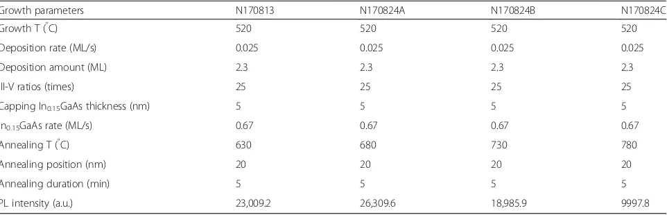
In this study, the quantum dot structure is grown on GaAs (001) (N+) substrates in a Veeco Gen 930 MBE system. Annealing temperature has been investigated, and the annealing temperatures for these four samples (N170813, N170824A-N17084C) are 630, 680, 730, and 780 °C, respectively. The growth parameters of quantum dots of these four samples have exactly the same (Table1).
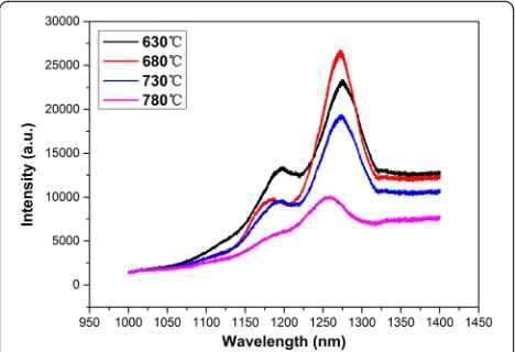
Photoluminescence (PL) measurements were con-ducted for the four samples. With the increase of an-nealing temperature, the strongest PL intensity was achieved at the annealing temperature of 680 °C (as shown in Fig. 1). This is because that arsenic (As) and Ga are desorbed as the annealing temperature rises higher. That process can create more defects, and the lattice of InAs quantum dots has changed at high temperature.
Quantum dot laser active area has been optimized at the low arsenic pressure of 4 × 10⁻⁷Torr [16] and low growth rate of 0.025 ML/s. After annealing, we found
that the wavelength was less than 1300 nm; therefore, we fine-tuned the growth conditions. A 2.5 monolayer (ML) thick InAs was grown at 520 °C and capped by a 5-nm thick In0.15Ga0.85As strain-reducing layer at the
same temperature. This layer was followed by a 15-nm GaAs layer which deposited at a lower temperature (LT) of 520 °C. Then, we grew the final 20-nm GaAs layer at a higher temperature (HT) of 630 °C (as shown in Fig.2a).
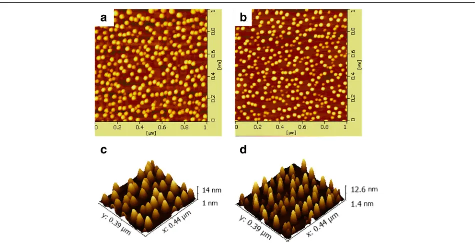
The PL spectrum and the atomic force microscopy (AFM) images of the surface of the QDs were measured for the test sample. The emission peak of 1308 nm is due to the ground-state transition, and the full width of half maximum (FWHM) of the peak is about 31 nm (as shown in Fig.2b). We grew a layer of bare quantum dots on the buried layer of five layers in the test sample to carry out the AFM measurement. The growth conditions are exactly the same as the buried quantum dots de-scribed before. The AFM image of the surface of the QDs shows that the QD density of the annealed sample is about 3.2 × 1010 cm−2 (as shown in Fig. 3a). The quantum dot has an average height of 8 nm. On the contrary, the unannealed quantum dot sample’s size and distribution are not uniform. Bimodal size can be seen and QD density is about 2.9 × 1010 cm−2. The quantum dot has a height of 5–7 nm (as shown in Fig.3b).
[image:2.595.58.539.577.732.2]During the epitaxial growth of a 1.3-μm quantum dot laser, the bimodal-size of InAs quantum dots can be well eliminated through the single-layer annealing for the laser active area. Compared with the sample grown with-out annealing (as shown in Fig. 3c), the sample grown with an annealing temperature at 680 °C (as shown in Fig.3d) has a higher quantum dot density and a uniform quantum dot size. That can be attributed to the follow-ing reasons. At first, GaAs cap layer grows immediately after the growth of InAs quantum dots, so it can only grow at a low temperature, which reduces the lattice quality of GaAs and introduces defects. High-temperature annealing
Table 1Comparison of several types of growth parameters and annealing temperatures
Growth parameters N170813 N170824A N170824B N170824C
Growth T (°C) 520 520 520 520
Deposition rate (ML/s) 0.025 0.025 0.025 0.025
Deposition amount (ML) 2.3 2.3 2.3 2.3
III-V ratios (times) 25 25 25 25
Capping In0.15GaAs thickness (nm) 5 5 5 5
In0.15GaAs rate (ML/s) 0.67 0.67 0.67 0.67
Annealing T (°C) 630 680 730 780
Annealing position (nm) 20 20 20 20
Annealing duration (min) 5 5 5 5
can eliminate defects and can grow high-quality GaAs cap layer used to continue growing InAs quantum dots. In addition, the dislocations are generated during InAs/GaAs heteroepitaxy, in situ single-layer annealing can eliminate dislocation or change the dislocation growth direction and then improve the quality of InAs quantum dots.
Device Design and Preparation
The laser’s structure consisted of a GaAs layer embed-ded with five layers of self-assembled InAs QD core layers. The 200-nm n-waveguide layer and p-waveguide layer were grown on top and bottom of the QD struc-ture. The QD active region and waveguide layer were sandwiched by two 1.8-μm p-type (Be: 4E18) and n-type (Si: 2E18) Al0.45Ga0.55As layers. A 200-nm p+ GaAs (Be:
3E19) layer was deposited for electrical contact (as shown in Fig.4a).
A small part of the wafer is etched by chemical etching to thin the upper cladding layer with H3PO4-H2O2-H2O
(1:1:4) after the laser epitaxial structure was completed [17,18]. It can be seen that the PL spectrum of this sam-ple has a central wavelength of 1294 nm (as shown in Fig. 4b). The blue shift of the center wavelength com-pared to the abovementioned test sample (as shown in Fig.2a) is due to the high-temperature growth (650 °C) during the growth step of the upper cladding with a growth time longer than 2 h. It also may be from the in-dium (In) component of the In0.15GaAs cap layer’s rock
drifts.
The InAs/GaAs QD laser wafer was coated with photoresist to define the surface pattern. The first edi-tion of photolithography forms a ridge pattern of 100 μm. The ridge waveguide was fabricated by induct-ively coupled plasma (ICP) etching with an etching depth of 2μm, followed by Plasma Enhanced Chemical
Vapor Deposition (PECVD) in order to form SiO2
insulation. In the next step, we made a contact window of 90 μm in width on the ridge for current injection. Then Ti/Pt/Au 51 nm/94.7 nm/1122 nm was deposited as a p-type electrode with magnetron sputtering (as shown in Fig.5). The wafer is thinned to 120μm, and a 50-nm thick AuGeNi (80:10:10 wt% alloy) with a 300-nm thick Au layer was deposited on the back of the wafer, using thermal evaporation for n-type electrode [19, 20]. The entire sample was annealed at 460 °C for 10 s in order to form an ohmic contact. During the whole fabrication process, the sample was cleaned se-quentially with acetone and isopropyl alcohol and rinsed with deionized water.
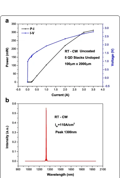
The electrical and optical properties of the device were measured when the laser was finished. Power-current-voltage (P−I−V) characteristics of broad area lasers were tested in the continuous wave (CW) at RT. The threshold current density of the laser is 110
A/cm2 (as shown in Fig. 6a), and the central
Fig. 1Comparison of photoluminescence (PL) spectra of epitaxial
wafers under different annealing temperature
Fig. 2The active region structure and PL spectrum.aThe structure of the undoped QD laser active region.bPL spectrum of the QD laser active
[image:3.595.57.291.88.248.2] [image:3.595.58.540.543.704.2]wavelength of the lasing spectrum is 1.3 μm (as shown in Fig. 6b). It can be seen from the lasing spectrum that the central wavelength of the laser at room temperature is redshifted because of heating ef-fect of the laser operation. In this study, the laser can continuously lase at room temperature and reach a good threshold current density as well as a good out-put power without facet coating and undoping in the active region, which indicates the high crystal quality of the laser. The single-layer annealing method has a certain effect on the bimodal size quantum dot
system. Deeper level research will be further studied based on this to further improve the density of QDs, in order to achieve a lower threshold current, lower power consumption, higher output power, and high char-acteristic temperature.
Conclusions
A series of optimizations of the growth parameters of high-density quantum dots were investigated. The single-layer annealing method was used to successfully suppress the formation of the bimodal-size system of
Fig. 3AFM images of the InAs/GaAs QDs.aSingle layer high-temperature annealing.bNo annealing.c3D small area size distribution image with
high-temperature annealing.d3D small area size distribution image without annealing
Fig. 4Device structure.a1.3-μm quantum dot F-P broad area laser's epitaxial structure.bPL spectrum of the QDs laser's epitaxial structure at RT.
[image:4.595.61.536.86.329.2] [image:4.595.57.540.542.701.2]quantum dots. We studied the annealing temperature and annealing layer position in detail. An optimized an-nealing temperature of 680 °C and a distance from the quantum dot layer of 20 nm were obtained. A threshold current density of 110 A/cm2 has been achieved for a 1.3-μm InAs/GaAs QD F-P laser at room temperature and continuous-wave operation with a lasing wavelength of 1.3μm.
Abbreviations
AFM:Atomic Force Microscope; Annealing T: Annealing temperature;
CW: Continuous wave; F-P: Fabry–Perot; FWHM: Full width at half maximum;
Growth T: Growth temperature; HT: High temperature; LT: Low temperature; MBE: Molecular beam epitaxy; PL: Photoluminescence; QD: Quantum dot; RT: Room temperature; SEM: Scanning electron microscope; WPE: Wall plug efficiency
Acknowledgements
We appreciated Professor of Xiao-Qiang Feng and Dr. Xiang-Jun Shang for polishing the manuscript.
Funding
This work is supported by the National Natural Science Foundation of China (61435012, 61505196), the National 973 program (2014CB643903,
2013CB933304), the Open Fund of High Power Laser Lab, China Academy of Engineering Physics (Grant No. 2013HEL03), and Shanxi Province
International Science and Technology Cooperation and Exchange Project (2016KW-040).
Availability of Data and Materials
We declared that materials described in the manuscript, including all relevant raw data, will be freely available to any scientist wishing to use them for non-commercial purposes, without breaching participant confidentiality.
Authors’Contributions
X-BS grew the samples, carried out the alignment, took part in discussions and in the interpretation of the result, and wrote the manuscript. YD and BM participated in the design of the study and discussions of the results. K-LZ and Z-SC helped in the technical support for the characterizations and the reconstruction of the data. J-LL and X-RC co-supervised the writing of the manuscript. Y-QX, YD, H-QN, and Z-CN supervised the writing of the manuscript and the experimental part. YD edited the manuscript. All the authors have read and approved the final manuscript.
Authors’Information
X-BS is a master student of Institute of Photonics and Photonic Technology, Northwest University. Ying Ding is a professor of Institute of Photonics and Photonic Technology, Northwest University. Ben Ma is a PhD student of the Institute of Semiconductors, Chinese Academy of Sciences. K-LZ and Z-SC are students of School of Physics and Nuclear Energy Engineering, Beihang Univer-sity. J-LL is a PhD student of Dept. of Missile Engineering, Shijiazhuang Campus, Army Engineering University. X-RC is a master student of Wide Bandgap Semi-conductor Technology Disciplines State Key Laboratory, Xidian University. Y-QX, H-QN, and Z-CN are professors of the Institute of Semiconductors, Chinese Academy of Sciences.
X-BS, K-LZ, Z-SC, J-LL, and X-RC also work at the Institute of Semiconductors, Chinese Academy of Sciences.
Competing Interests
The authors declare that they have no competing interests.
Author details
1National Key Laboratory of Photoelectric Technology and Functional
Materials (Culture Base), Institute of Photonics and Photonic Technology, Northwest University, Xi’an 710069, China.2State Key Laboratory for Superlattices and Microstructures, Institute of Semiconductors, Chinese Academy of Sciences, Beijing 100083, China.3College of Materials Science and Opto-Electronic Technology, University of Chinese Academy of Sciences, Beijing 100083, China.4Department of Missile Engineering, Shijiazhuang
Fig. 5SEM image of the laser's cross section. The F-P broad area laser with
a standard laser fabrication process. GaAs/AlGaAs etch depth is about 2-μm. The PECVD formed SiO2is 260 nm
Fig. 6Device measurements.aP-I-V curves of a QD laser.bThe lasing
[image:5.595.57.290.86.292.2] [image:5.595.56.291.357.705.2]Campus, Army Engineering University, Shijiazhuang 050003, China.5School of Physics and Nuclear Energy Engineering, Beihang University, Beijing 100191, China.6Wide Bandgap Semiconductor Technology Disciplines State Key Laboratory, Xidian University, Xi’an 710071, China.
Received: 3 January 2018 Accepted: 9 February 2018
References
1. Kaizu T, Yamaguchi K (2001) Self size-limiting process of InAs quantum dots grown by molecular beam epitaxy. Jpn J Appl Phys 40(40):1885–1887
2. Wasilewski ZR, Fafard S, Mccaffrey JP (1999) Size and shape engineering
of vertically stacked self-assembled quantum dots. J Cryst Growth 201(5):1131–1135.
3. Tanabe K, Rae T, Watanabe K et al (2013) High-temperature 1.3μm InAs/ GaAs quantum dot lasers on Si substrates fabricated by wafer bonding. Appl Phys Express 6(6):2703.
4. Wang H, Kong L, Pan J, Xu T, Wei J, Haiqiao N, Bifeng C, Ying D (2013) Recent progress of semiconductor mode-locked lasers. Laser Opto Electron Prog 5:050001-1–050001-14.
5. Ledentsov NN, Grundmann M, Kirstaedter N et al (1996) Ordered arrays of quantum dots: formation, electronic spectra, relaxation phenomena, lasing. Solid State Electron 40(1–8):785–798.
6. Joyce PB, Krzyzewski TJ, Bell GR et al (2000) Effect of growth rate on the size, composition, and optical properties of InAs/GaAs quantum dots grown by molecular-beam epitaxy. Phys Rev B Condens Matter 62(62):10891–10895.
7. Nakata Y, Mukai K, Sugawara M et al (2000) Molecular beam epitaxial growth of InAs self-assembled quantum dots with light-emission at 1.3μm. J Cryst Growth 208(1):93–99.
8. Mukhametzhanov I, Heitz R, Zeng J et al (1998) Independent manipulation
of density and size of stress-driven self-assembled quantum dots. Appl Phys Lett 73(13):1841–1843.
9. Medeiros-Ribeiro G, Leonard D, Petroff PM (1995) Electron and hole
energy levels in InAs self-assembled quantum dots. Appl Phys Lett 66(14):1767–1769.
10. Kaida R, Akiyama T, Nakamura K et al (2016) Theoretical study for misfit dislocation formation at InAs/GaAs(001) interface. J Cryst Growth, 468: 919-922.
11. Wang YQ, Wang ZL, Shen JJ et al (2002) Engineering vertically aligned InAs/ GaAs quantum dot structures via anion exchange. Solid State Commun 122(10):553–556.
12. Passow T, Li S, Feinäugle P et al (2007) Systematic investigation into the influence of growth conditions on InAs/GaAs quantum dot properties. J Appl Phys 102(7):716.
13. Ito T, Hirai K, Akiyama T et al (2013) Ab initio-based approach to novel behavior of InAs wetting layer surface grown on GaAs(001). J Cryst Growth 378(17):13–16.
14. Chen S, Tang M, Jiang Q et al (2014) InAs/GaAs quantum-dot superluminescent light-emitting diode monolithically grown on a Si substrate. ACS Photonics 1(7):638–642.
15. Shimomura K, Kamiya I (2015) Strain engineering of quantum dots for long wavelength emission: photoluminescence from self-assembled InAs quantum dots grown on GaAs(001) at wavelengths over 1.55μm. Appl Phys Lett 106(8):2815.
16. Sugaya T, Amano T, Komori K (2006) Improved optical properties of InAs quantum dots grown with an As2 source using molecular beam epitaxy. J Appl Phys 100(6):1753.
17. Yamaguchi K, Yujobo K, Kaizu T (2000) Stranski-Krastanov growth of
InAs quantum dots with narrow size distribution. Jpn J Appl Phys 39(12A):L1245–L1248.
18. Mori Y, Watanabe N (1978) A new etching solution system, H 3 PO 4-H 2 O 2-H 2 O, for GaAs and its kinetics. J Electrochem Soc 125(9):1510-1514. 19. Ishida M, Hatori N, Otsubo K et al (2007) Low-driving-current
temperature-stable 10 Gbit/s operation of p-doped 1.3μm quantum dot lasers between 20 and 90/spldeg/C. Electron Lett 43(4):219–221.