N A N O E X P R E S S
Open Access
The coupling between localized surface plasmons
and excitons via Purcell effect
Feng Wang, Dongsheng Li
*, Deren Yang and Duanlin Que
Abstract
The coupling between localized surface plasmons (LSPs) within silver nanostructures and excitons in a silicon-rich silicon nitride (SiNx) matrix has been demonstrated via the Purcell effect. A simple model is employed for the estimation of the Purcell factor as well as the average position of excitons within a luminescence matrix. The estimated average position of the excitons is located at approximately 40 nm beneath the top surface of the SiNx films. The approaches for further improving the optoelectrical properties of the luminescence matrix are anticipated based on the model we adopted. The optimization of the thickness of the luminescence matrix as well as the size and shape of metal nanostructures may be the alternative approaches. Besides, the application of multilayers with the luminescence matrix inserted between barrier layers (we defined it as confined structures here) may be also an available choice. Our work may provide a deep comprehension on the coupling between LSPs and excitons, which is not limited to a certain luminescence material but with unconfined structures.
Keywords:Localized surface plasmons, Silicon-rich silicon nitride, Silver nanostructures, Average position of excitons, Luminescence
Background
As an effective approach to overcome the diffraction limit of classical optics due to the mismatch of energy and momentum between electrons and photons, loca-lized surface plasmons (LSPs) referring to the collective electronic oscillations within the metallic nanostructures excited by the external radiation have captured much re-search interest [1-8]. The confinement of electromag-netic field at the subwavelength volume as well as the Purcell enhancement of this field on the order of the quality factor (Q) of the LSP resonance is achieved by the adoption of these polariton modes [9,10]. This Pur-cell enhancement effect is similar to the PurPur-cell effect in a microcavity with a quality factorQ, where the coupling between an exciton and a microcavity mode is allowed by the field confinement within an ultrasmall volume V [10,11]. This effect can enhance the density of photon states, which is proportional to the spontaneous emis-sion decay rate, leading to the Purcell factor (Fp) en-hancement of luminescence [10,12]. Obviously, this Fp
can characterize the coupling efficiency indirectly, which is influenced especially by the sizes and species of metallic nanostructures, the energy of emitted photons (hνD= hc/λD), and the distance (d) between LSPs and excitons in a luminescence matrix [13]. The effects of these parameters onFpas well as the estimation of the average position of excitons within the luminescence matrix are particularly important for the further optimization of the lumines-cence properties of the active matrix.
In this letter, an amorphous silicon-rich silicon nitride (SiNx) film, a promising candidate material of silicon-based light sources due to its superior photo-physical properties [12,14-18], is employed as the luminescence matrix investigated here. Silver (Ag) nanostructures are used for the demonstration of the coupling between LSPs and excitons in SiNxdue to their lowest absorption losses and a superior enhancement of the local electromag-netic field among all the metals with plasmon resonances at visible frequency, which is near the luminescence wave-length of SiNxfilms. Both the relationships betweenFpand
λD and the estimation of the average position (d) of the excitons within SiNx are provided based on a simple model.
* Correspondence:[email protected]
State Key Laboratory of Silicon Materials and Department of Materials Science and Engineering, Zhejiang University, Hangzhou 310027, People’s Republic of China
Methods
SiNxfilms with a thickness of approximately 50 nm were deposited using a plasma-enhanced chemical vapor de-position technique onto the substrates of p-type Si (100) or quartz for various measurements. The preparation of SiNx films has been described in detail in our previous paper [12]. After the deposition of SiNx, a Ag layer was deposited by magnetron sputtering, with the thickness regulated by the sputtering time (20, 40, 60, and 80 s). To form the Ag nanostructures with various dimensions and surface morphologies, a rapid thermal annealing (RTA) in argon at 500°C for 60 s was employed subse-quently. We label the samples by the sputtering time of the Ag layer, e.g., Ag40 refers to the sample with the sputtering time of the Ag layer of 40 s. A SiNxfilm with-out Ag was also fabricated as the reference sample (Ag0).
The ellipsometric parameters ψ and Δ can be obtained from the ellipsometric measurement (M-2000D, J. A. Wool-lam Co. Inc., Lincoln, NE, USA), from which the complex index of refraction (n) can be calculated using the equation
ofn¼
ffiffiffiffiffiffiffiffiffiffiffiffiffiffiffiffiffiffiffiffiffiffiffiffiffiffiffiffiffiffiffiffiffiffiffiffiffiffiffiffiffiffiffiffiffiffiffiffiffiffiffiffiffiffiffiffiffiffiffiffiffiffiffiffiffiffi
14 sin2θ 0
ð Þtanð ÞψejΔþ2 tanð ÞψejΔþtan2ð ÞψejΔ
p
n0sinð Þθ0
cosð Þθ0½1þtanð ÞψejΔ , where
θ0andn0stand for the angle of incidence and the complex refractive index of the ambient, respectively [19]. Meanwhile, the film thickness (t) can be obtained from the equation of
t¼ jlnej
2β
ð Þλ
4πncosð Þθ1 , where β¼2π
t λ
ffiffiffiffiffiffiffiffiffiffiffiffiffiffiffiffiffiffiffiffiffiffiffiffiffiffiffiffiffiffiffiffi
n2n2
0sin2ð Þθ0
q
and θ1 represents the angle of refraction [19]. All these calcula-tions, including the determination of the extinction coef-ficient (k) as a function of wavelength, have been integrated into the ellipsometric measurement system. Consequently, we can acquire the data oft,n, andk dir-ectly from ellipsometry by scanning over the angle (θ0) range from 65° to 75° in steps of 5° with the spectral (λ) range from 400 to 800 nm. The extinction spectra of the samples with and without Ag nanostructures were obtained using a Hitachi U-4100 spectrophotometer (Hitachi, Ltd., Chiyoda, Tokyo, Japan). The photolumi-nescence (PL) spectra of all the samples were excited by a 325-nm He-Cd laser using an Acton SpectraPro-2500i monochrometer (Acton Research Corporation, Acton, MA, USA).
Results and discussion
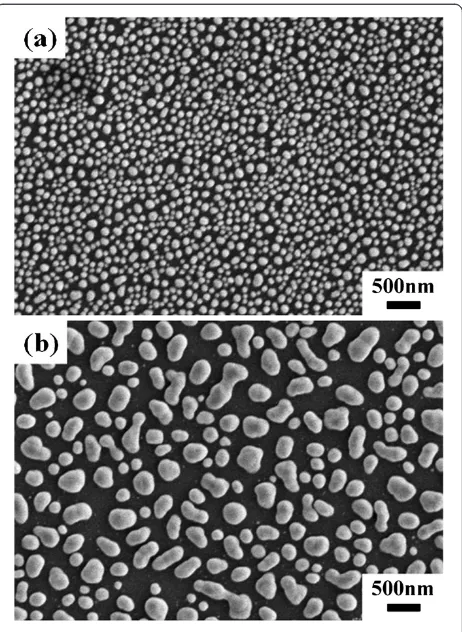
Figure 1 shows the scanning electron microscopy (SEM; Hitachi S-4800, Hitachi, Ltd.) images of Ag nanostruc-tures with sputtering times of 40 and 80 s after the treat-ment of RTA. Dense Ag island films were obtained before the RTA process, where the sizes of Ag nanos-tructures were a little smaller than those with the RTA procedure. From the incomplete statistics, we obtained the radii (r0) of Ag40 and Ag80 as approximately 45 nm and approximately 110 nm, respectively. The larger size
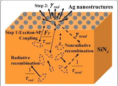
of the sample Ag80 might originate from the larger ori-ginal size of the as-deposited Ag island film for Ag80. After the Ostwald ripening process [20], larger Ag parti-cles could be obtained for the sample with a sputtering time of 80s than that with a sputtering of 40s. As have been investigated, the addition of Ag nanostructures can improve the luminescence efficiency of the active matrix [12]. It might result from the significant enhancement of the local electromagnetic field induced by the collective oscillation of excited free electrons surrounding the Ag nanostructures [11-13]. This enhanced local electromag-netic field will provide an additional path of recombin-ation due to the high mode density in the LSP, from which the spontaneous emission rate can be increased significantly via the Purcell effect [11,12]. A possible mechanism of the LSP-exciton coupling is shown in Figure 2.
Coupling between localized surface plasmons and excitons via Purcell effect
For the sample without the coverage of Ag nanostruc-tures, the excitons generated in SiNx films by optical or electrical pumping are terminated by radiative or
[image:2.595.307.538.88.404.2]nonra-diative recombination with the internal quantum
efficiency (ηint) determined by the ratio of the radiative recombination rates (κrad) to the nonradiative recombin-ation rates (κnrad) as ηint=κrad/ (κrad+κnrad) = τrad−1/(τrad−1 + τnrad−1 ). After the addition of Ag nanostructures, the interaction between LSPs and excitons can be treated as a two-step process (shown in Figure 2). When the energy (ћωex) of excitons is close to the electron vibration energy (ћωSP) of LSPs, the excitons transfer their energies to the LSP modes with the radiative recombination rates (κrad) enhanced by the Purcell factorFp[4,11]. This process will compete with the nonradiative decay and enhance the PL decay rate (κPL) significantly due to the large electromag-netic fields introduced by the high mode density in LSPs [21]. For the second step, the energy from the LSP mode will be out-coupled to radiated photons with the rateγrad, as shown in Figure 2. This coupling will compete with the nonradiative loss (γnrad) due to the absorption of Ag nanostructures, where the coupling efficiency can be defined asηc=γrad/ (γrad+γnrad) [22]. This efficiency (ηc) can be optimized via the modulation of the parameters of metal nanostructures, such as the size, shape, density, and the distance between metal nanostructures [22].
As has been mentioned above, the Purcell factor Fp can be used to characterize the efficiency of coupling into the SP mode [11,12,22] estimated as the ratio of the effective density of the SP modesρSPto that of the radi-ation componentsρrad[23]. For the dipole placed at the distancedfrom the particle bottom surface and oriented in thezdirection normal to the surface, the value ofρSP is given by [22,23]
ρSP¼ Lð Þω
Veff r0 r0þd
6
ð1Þ
where the normalized line shape of the dipole oscillation L(ω) is
Lð Þ ¼ω Im ðεMð Þ þω 2εDÞ 1
Z
Im ðεMð Þ þω 2εDÞ1
dω
ð2Þ
withεMandεDbeing the dielectric constant of the metal and surrounding media, respectively, which can be acquired from the ellipsometric data. A simple model is used for the estimation of the effective volumeVeffof SP modes, where the shape of the Ag nanostructures is a sphere in approximate with the radii (r0) equal to 45 and 110 nm for Ag40 and Ag80, respectively. The values of Veffcan be obtained via the following equation [22]:
Veff ¼
ZZZ
r<r0
1 2ε0
∂ðωεMÞ
∂ω Ein2d3rþ
ZZZ
r>r0
1 2ε0εDE
2 outd3r
1 2ε0εDE
2 max
¼4
3πr 3 0 1þ
1 2ε0
ð3Þ where the dipole field inside (Ein) and outside (Eout) of the metal sphere with radiusr0can be obtained by solv-ing the Laplace equation with proper boundary condi-tions at r = r0 [24]. The maximum dipole field (Emax) occurs at the surface of the metal nanostructures for this model. The value ofρradis described as follows [22]:
ρrad¼ 1 3π2
2π
λD 1
ω ð4Þ
with λD being the emission wavelength in the SiNx
matrix. Combining Equations 1 to 4, the Purcell factor can be obtained by
Fpð Þ ¼ω ρρSP rad
¼Lð Þω
Veff r0 r0þd
6
1 3π2
2π
λD 3
1
ω " #1
ð5Þ
[image:3.595.56.291.90.262.2]Besides the parameters of the Ag nanostructures which will alter the values of ρSP, both the distance (d) between the metal nanostructures and the excitons in SiNx and the emission wavelength (λD) of the lumines-cence matrix will influence the values of Fp. Therefore, the influences of λD and d accompanied with the size (r0) of the Ag nanostructures on the values of Fp are simulated, as shown in Figure 3. By fixing the value ofd, the influence ofλDonFpfor Ag40 is compared with that for Ag80, as shown in Figure 3a,b. Obviously, the values ofFpare increased with the emission wavelength follow-ing the relationship of Fp∝λD3 in both the cases. It means that the Purcell enhancement may be more con-spicuous for the luminescence matrix with longer
Figure 2Schematic diagram of the electron–hole
recombination and coupling mechanism between LSPs and excitons in SiNx.The interaction between LSPs and excitons can be
emission wavelength. A larger value of Fp for Ag40 is obtained compared to that for Ag80, which may result from the predomination of the volume termr03in
Equa-tion 5 over the factor r0
r0þd
6
here. It is clear that more
[image:4.595.61.538.89.337.2]effective LSP-exciton coupling can be achieved for Ag40 compared to Ag80. The influences of d on Fp are also checked in both Ag40 and Ag80 by setting the emission wavelength at 600 nm, as shown in Figure 3c,d. The values of Fp are increased with the decrease of d, and
Figure 3The Purcell factors with different emission wavelengths and different LSP-exciton coupling distances.(a) and (c) stand for Ag40, and (b) and (d) stand for Ag80. Both the distance between the Ag nanostructures and the excitons in SiNxand the emission wavelength of the SiNxmatrix will influence the values of the Purcell factor.
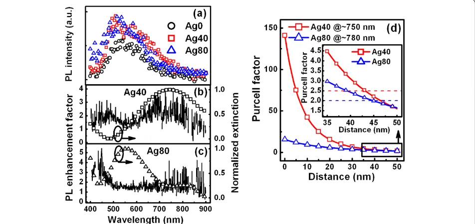
Figure 4The LSP resonance effects and the determination of the average position of excitons in SiNx.(a) PL spectra for the samples with
and without Ag nanostructures. PL enhancement factor (left axis) accompanied with the extinction spectra (right axis) for (b) Ag40 and (c) Ag80. (d) The Purcell factors vs. distance for Ag40 atλD= 750 nm and Ag80 atλD= 780 nm. The average position of excitons is located at 43 to 45 nm
[image:4.595.62.538.458.683.2]this increase is more obvious in Ag40 than that in Ag80. The influence of d may be much more significant than that ofλDonFpfor the SiNxmatrix investigated here.
Average position of excitons in SiNxmatrix
From the discussions above, we can estimate the average position of excitons in the luminescence matrix with un-confined structures (the un-confined structure referred to the one with the active matrix inserted between two bar-rier layers) and optimize their luminescence properties conveniently based on this model. These matrixes may be SiOx, SiNx, Si nanocrystals within SiOxor SiNx, ZnO, (In)GaN, and so on. For the estimation of the average position of excitons in our SiNx matrix, PL spectra are measured for the determination of the value of λD, as shown in Figure 4a. Broadband emission range from approximately 400 nm to approximately 850 nm with the central wavelength of approximately 600 nm could be observed. By dividing the PL intensity of Ag40 or Ag80 to that of Ag0, the PL enhancement factor (FPL) can be obtained. As can be seen in Figure 4b,c (left axis), two obvious peaks of theFPLcan be resolved, where the peak with shorter wavelength is induced by the improve-ment of light extraction from the active layer due to the minimum absorption of the Ag nanostructures. The peak with longer wavelength results from the coupling between LSPs and excitons in SiNxconfirmed by the ex-tinction spectra, shown in Figure 4b,c (right axis), due to the consistence between this peak and the one of the di-pole resonance, which is enhanced by the Purcell factor Fp[11]. Obviously, the dipolar resonance peak of the Ag nanostructures redshifts gradually with the increase of their sizes. Correspondingly, the FPL is located at ap-proximately 750 nm with the value of apap-proximately 2.5 for Ag40 and at approximately 780 nm with the value of approximately 2.0 for Ag80.
To find out the relationship between Fp and FPL, the originations of these two factors are considered. Both of them mainly result from the enhancement of the spon-taneous emission rate, where the value ofFp can be re-written as Fp(ω) =κPL* (ω)/κPL(ω), withκPL(ω) and κPL* (ω) standing for the original and enhanced PL decay rates, respectively [25] . Consequently, the approximation rela-tion betweenFpandFPL (FP≈ FPL) can be employed for the estimation of the average position of excitons (d) in SiNxby plotting the curves ofFpvs.dat the wavelength where the enhancement of dipole resonance occurred, as shown in Figure 4d. The average position of excitons is located at 43 to 45 nm beneath the top surface of the SiNx films. Consequently, the optimized luminescence properties can be achieved via the optimization of para-meters in the Equation 5 by the modulation of the sizes and shape of the Ag nanostructures. Both the optimal PL and electroluminescence efficiency of a SiNx-based
light-emitting device are achieved by the addition of Ag nanostructures with the radii of approximately 50 nm from our experimental results (not shown here). Further attentions can be paid to the decrease of the distance be-tween LSPs and excitons, which may be achieved via the optimization of the thickness of the luminescence matrix as well as the appropriate design of the luminescence structure. Multilayers with the active matrix inserted between barrier layers may be also an available choice.
Conclusions
The coupling between LSPs and excitons in SiNx has
been demonstrated via the Purcell effect. When the energy of the excitons is close to the electron vibration energy of LSPs, the excitons can transfer their energy to the LSPs, in which the radiative recombination rates are enhanced by the Purcell factor. The relationships between the Purcell factors and the deposition parameters are illustrated, in-cluding the size of the Ag nanostructures, the energy of the emitted photons, and the distance between the LSPs and excitons in the SiNxmatrix. Further improvement on the luminescence efficiency can be achieved by decreasing the distance between LSPs and excitons and/or modulat-ing the parameters of the metal nanostructures.
Abbreviations
Ag: silver;FPL: PL enhancement factor;Fp: Purcell factor; LSPs: localized surface plasmons; PL: photoluminescence; RTA: rapid thermal annealing; SEM: scanning electron microscopy; SiNx: silicon-rich silicon nitride;
SiOx: silicon oxide.
Competing interests
The authors declare that they have no competing interests.
Authors’contributions
FW performed the experiments, collected and analyzed the data, and wrote the paper. DL conceived the experiments, analyzed the results, and wrote the paper. DY and DQ helped with the data analysis and wrote the paper. All authors read and approved the final manuscript.
Acknowledgments
The authors thank the National Natural Science Foundation of China (no. 61176117), the 863 Program (no. 2011AA050517), and the Innovation Team Project of Zhejiang Province (no. 2009R5005).
Received: 17 October 2012 Accepted: 22 November 2012 Published: 7 December 2012
References
1. Maier SA, Brongersma ML, Kik PG, Meltzer S, Requicha AAG, Atwater HA:
Plasmonics - a route to nanoscale optical devices.Adv Mater2001,
19:1501–1505.
2. Barnes WL, Dereux A, Ebbesen TW:Surface plasmon subwavelength optics.Nature2003,424:824–830.
3. Ozbay E:Plasmonics: merging photonics and electronics at nanoscale dimensions.Science2006,311:189–193.
4. Walters RJ, Van Loon RVA, Brunets I, Schmitz J, Polman A:A silicon-based electrical source of surface plasmon polaritons.Nat Mater2010,9:21–25. 5. Bharadwaj P, Bouhelier A, Novotny L:Electrical excitation of surface
plasmons.Phys Rev Lett2011,106:226802.
6. Cai W, Vasudev AP, Brongersma ML:Electrically controlled nonlinear generation of light with plasmonics.Science2011,333:1720–1723. 7. Pleros N, Kriezis EE, Vyrsokinos K:Optical interconnects using plasmonics
8. Luo Y, Lei DY, Maier SA, Pendry JB:Broadband light harvesting nanostructures robust to edge bluntness.Phys Rev Lett2012,108:023901. 9. Kravets VG, Zoriniants G, Burrows CP, Schedin F, Casiraghi C, Klar P, Geim
AK, Barnes WL, Grigorenko AN:Cascaded optical field enhancement in composite plasmonic nanostructures.Phys Rev Lett2010,105:246806. 10. Tanaka K, Plum E, Ou JY, Uchino T, Zheludev NI:Multifold enhancement of
quantum dot luminescence in plasmonic metamaterials.Phys Rev Lett 2010,105:227403.
11. Purcell M:Spontaneous emission probabilities at radio frequencies.Phys Rev1946,69:681.
12. Wang F, Li D, Yang D, Que D:Enhancement of light-extraction efficiency of SiNxlight emitting devices through a rough Ag island film.Appl Phys Lett2012,100:031113.
13. Hutter E, Fendler JH:Exploitation of localized surface plasmon resonance.
Adv Mater2004,19:1685–1706.
14. Cen ZH, Chen TP, Ding L, Liu Y, Wong JI, Yang M, Liu Z, Goh WP, Zhu FR, Fung S:Strong violet and green-yellow electroluminescence from silicon nitride thin films multiply implanted with Si ions.Appl Phys Lett2009,
94:041102.
15. Huang R, Wang DQ, Ding HL, Wang X, Chen KJ, Xu J, Guo YQ, Song J, Ma ZY:Enhanced electroluminescence from SiN-based multilayer structure by laser crystallization of ultrathin amorphous Si-rich SiN layers.
Opt Express2010,18:1144–1150.
16. Jacques E, Pichon L, Debieu O, Gourbilleau F:Electrical behavior of MIS devices based on silicon nanoclusters embedded in SiOxNyand SiO2
films.Nanoscale Res Lett2011,6:170.
17. Cazzanelli M, Bianco F, Borga E, Pucker G, Ghulinyan M, Degoli E, Luppi E, Véniard V, Ossicini S, Modotto D, Wabnitz S, Pierobon R, Pavesi L: Second-harmonic generation in silicon waveguides strained by silicon nitride.
Nat Mater2012,11:148–154.
18. Minissale S, Yerci S, Negro LD:Nonlinear optical properties of low temperature annealed silicon-rich oxide and silicon-rich nitride materials for silicon photonics.Appl Phys Lett2012,100:021109.
19. Azzam RMA, Bashara NM:Ellipsometry and Polarized Light. 1st edition. Amsterdam: North-Holland Publishing Company; 1977.
20. Perez DP:Silver Nanoparticles. Vukovar: InTech; 2010.
21. Iwanaga M, Ikeda N, Sugimoto Y:Enhancement of local electromagnetic fields in plasmonic crystals of coaxial metallic nanostructures.
Phys Rev B2012,85:045427.
22. Sun G, Khurgin JB, Soref RA:Plasmonic light-emission enhancement with isolated metal nanoparticles and their coupled arrays.J Opt Soc Am B 2008,25:1748–1755.
23. Le KQ, Bienstman P:Optical modeling of plasmonic nanoparticles.
Plasmonics2011,6:53–57.
24. Jackson JD:Classical Electrodynamics. 3rd edition. New York: Wiley; 1962. 25. Okamoto K, Niki I, Scherer A, Narukawa Y, Mukai T, Kawakami Y:Surface plasmon enhanced spontaneous emission rate of InGaN/GaN quantum wells probed by time-resolved photoluminescence spectroscopy.
Appl Phys Lett2005,87:071102.
doi:10.1186/1556-276X-7-669
Cite this article as:Wanget al.:The coupling between localized surface plasmons and excitons via Purcell effect.Nanoscale Research Letters2012
7:669.
Submit your manuscript to a
journal and benefi t from:
7Convenient online submission
7Rigorous peer review
7Immediate publication on acceptance
7Open access: articles freely available online
7High visibility within the fi eld
7Retaining the copyright to your article